 International Workshop on Semiconductor Pixel Detectors for Particles and Imaging Grindelwald, Switzerland I. Tsurin, University of Liverpool Subject: design of planar silicon detectors for the Atlas upgrade (beneficial for the LHCb Ve. Lo upgrade R&D) - Detector layout: readout implants, guard structure, cut edge - Measurement instrumentation and methods - Some results (before irradiation) September 6 -10, 2010 1
 Long tradition in making silicon detectors for HEP SLHC challenges: Radiation Hardness Detector technology (research with e 2 v) Sensor layout (research with Micron Semiconductor) Detector environment: cooling, HV, readout etc. My subtask: Mask design for the planar silicon pixel (and strip) detectors to be manufactured in the UK by e 2 v and Micron Semiconductor To achieve good spatial resolution through efficient charge collection: - HV performance (main focus in this work) - Optimal implant geometry -> new RD 50 wafer 2
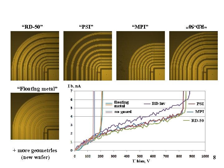
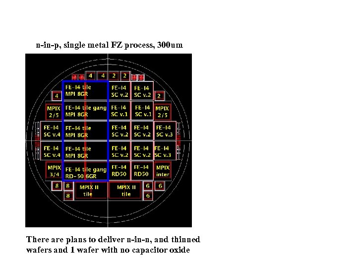
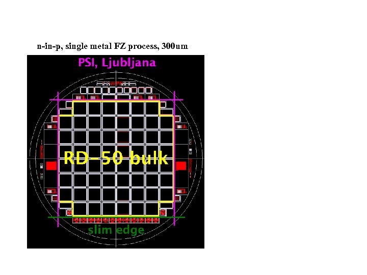
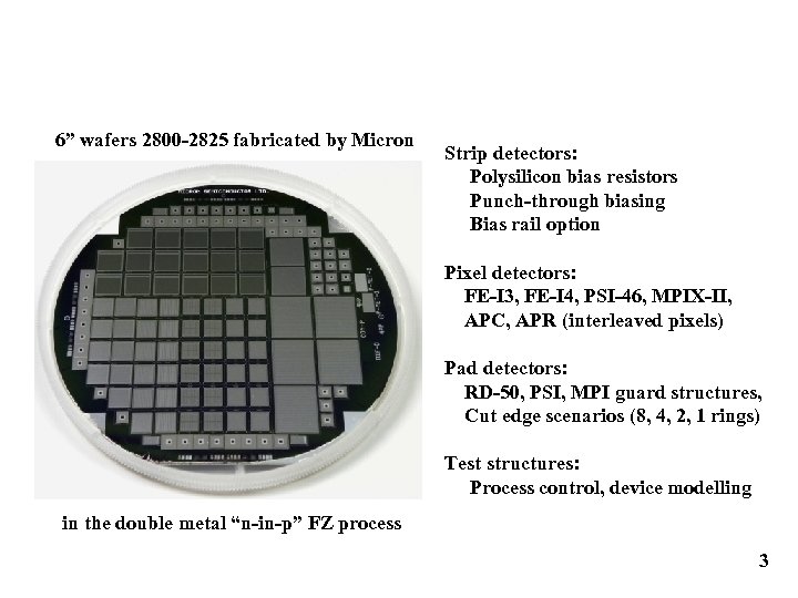 6” wafers 2800 -2825 fabricated by Micron Strip detectors: Polysilicon bias resistors Punch-through biasing Bias rail option Pixel detectors: FE-I 3, FE-I 4, PSI-46, MPIX-II, APC, APR (interleaved pixels) Pad detectors: RD-50, PSI, MPI guard structures, Cut edge scenarios (8, 4, 2, 1 rings) Test structures: Process control, device modelling in the double metal “n-in-p” FZ process 3
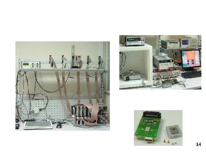
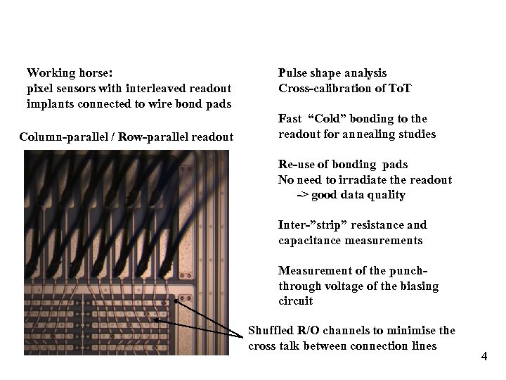 Working horse: pixel sensors with interleaved readout implants connected to wire bond pads Column-parallel / Row-parallel readout Pulse shape analysis Cross-calibration of To. T Fast “Cold” bonding to the readout for annealing studies Re-use of bonding pads No need to irradiate the readout -> good data quality Inter-”strip” resistance and capacitance measurements Measurement of the punchthrough voltage of the biasing circuit Shuffled R/O channels to minimise the cross talk between connection lines 4
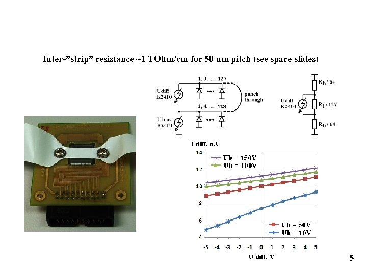 Inter-”strip” resistance ~1 TOhm/cm for 50 um pitch (see spare slides) 5
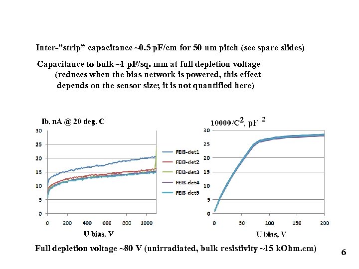 Inter-”strip” capacitance ~0. 5 p. F/cm for 50 um pitch (see spare slides) Capacitance to bulk ~1 p. F/sq. mm at full depletion voltage (reduces when the bias network is powered, this effect depends on the sensor size; it is not quantified here) Full depletion voltage ~80 V (unirradiated, bulk resistivity ~15 k. Ohm. cm) 6
 7
7
 “PSI” “MPI” “RD-50” “Floating metal” + more geometries (new wafer) 8
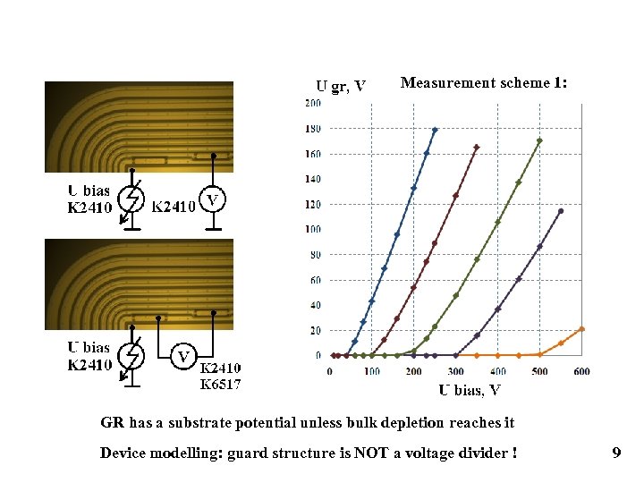 Measurement scheme 1: GR has a substrate potential unless bulk depletion reaches it Device modelling: guard structure is NOT a voltage divider ! 9
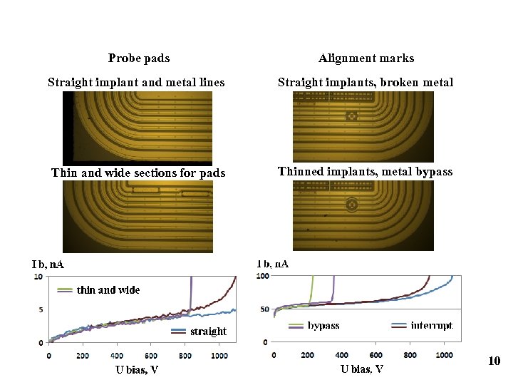 Probe pads Alignment marks Straight implant and metal lines Straight implants, broken metal Thin and wide sections for pads Thinned implants, metal bypass 10
 11
11
 12
12
 13
13
 14
14
 15
15
 Looks OK, but there is no guarantee. . .
 n-in-p, single metal FZ process, 300 um There are plans to deliver n-in-n, and thinned wafers and 1 wafer with no capacitor oxide
 n-in-p, single metal FZ process, 300 um