ec05b3fb48242f077874b7be4cb908a4.ppt
- Количество слайдов: 8
 Intelligent Design of Electronic Assets (IDEA) Workshop This is a 5 -10 minute public presentation providing a personal introduction and addressing one or more of the stated workshop objectives Alan Mishchenko Department of EECS UC Berkeley
 Self Introduction l l A professional researcher at the EECS Department, UC Berkeley Have been with UC Berkeley for about 15 years. During this time l l l l advanced from Assistant Researcher (2002) to Full Researcher (2013) co-authored 120+ peer-reviewed publications co-advised 20+ students participated in applying for and successfully completing 9 multi-year research projects funded by NSF/NSA/SRC facilitated unrestricted industrial donations from 10+ companies to support the research group Research interests: Efficient computation in logic synthesis and formal verification (recently look into HLS and hardware design) Have been developing and supporting ABC, an open-source synthesis and verification tool widely used in industry and academia Can be the Principal Investigator on research grants and a leader of research projects at Berkeley 2
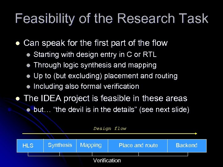 Feasibility of the Research Task l Can speak for the first part of the flow l l l Starting with design entry in C or RTL Through logic synthesis and mapping Up to (but excluding) placement and routing Including also formal verification The IDEA project is feasible in these areas l but… “the devil is in the details” (see next slide) Design flow HLS Synthesis Mapping Place and route Verification Backend
 Potential Problems l l For the flow to be fully automatic, it may be necessary to sacrifice too much quality The various iterations in the flow (for example, timing closure iterating re-synthesis, re-mapping, and incremental placement) may be problematic to automate Reusing the IP blocks may be hard to accomplish in the fully automated mode (without the designer providing detailed guidance on how to build timing/functionality interfaces) Fully automatic verification across the flow could be a major challenge (for example, industrial tools do not do a fully automated verification of the arithmetic data-path)
 Conclusion l The project is feasible but challenging l There are numerous potential problems l None of the problems seem to be a show-stopper l similar problems dogged design automation from its early days and have been addressed, with some degree of success, in other projects
 Background Material
 IDEA Workshop Background l l An exploratory technical workshop is being organized to discuss Intelligent Design of Electronic Assets (IDEA), a new initiative being developed by DARPA/MTO. The need for more computational power continues to increase for the vast majority of Do. D missions, including imaging, communication, electronic warfare, and radar, and access to low-cost custom integrated circuits is critical for next generation warfighter systems. A significant barrier to wide access to affordable, leading-edge integrated circuits is the cost and time associated with advanced integrated circuit (IC) design, driven by the need for large, highly skilled chip design teams and extensive manual verification. This problem is compounded for low-volume customers, such as the Do. D, academia and small businesses, where a significantly larger portion of IC cost is determined by design non-recurring engineering cost. IDEA is motivated by the desire to develop a validated and intelligent, low cost IC back-end design tool with no human in the loop. The overarching goal is to create a tool that performs all steps from RTL to GDS for use by teams with no chip design experience. On-going DARPA programs are making significant advances in reduction of chip design time through development of innovative methodology for subsets of the design process but still require high levels of human expertise. The workshop will serve as a forum for technical experts from the government, academia, and industry to discuss the potential for development of a completely automated cloud based design flow for converting RTL to GDS at a cost of less than $10, 000 per chip.
 IDEA Workshop Objectives l l l l To discuss the state of the art in EDA design flow and lessons learned in previous attempts to create “silicon compilers” and smart “ 24 -hour” design flows. To identify critical challenges to designing a generalized and completely automated low cost tool flow for converting RTL to GDS with no human in the loop. To identify IC and EDA performance tradeoffs that will lead to a simpler design flow while maintaining wide applicability. To identify existing standards and efforts that can be leveraged for IDEA’s success. To quantify the Do. D and commercial eco-system benefits of driving down the back-end cost of advanced integrated circuits. To identify compelling Do. D applications of an autonomous chip design tools as well as dual-use commercial applications. To establish potential program milestones and identify appropriate benchmarks to test and verify fabricated chips designed using the IDEA design tool. To discuss the viability of the $10 K/chip business model within the semiconductor ecosystem.


