7170e5a28c660cf4b015144f8b2470ac.ppt
- Количество слайдов: 59
 ID 027 C: The V 850/Fx 4 Timer Array Unit (TAU) and its Use for PWM Output Driver Diagnostics Renesas Electronics America Inc. Jeremy Brodt Senior Technical Applications Engineer 12 October 2010 Version 1. 1
 Jeremy Brodt Senior Technical Application Engineer n Responsible for 32 -bit Automotive Body MCUs l Development support l Product definition n Previous Experience: l Automated Systems Test Engineer for Body and Safety products at Delphi Electronics & Safety l MSCE from The University of Texas at Dallas l BSCE from Purdue University 2 © 2010 Renesas Electronics America Inc. All rights reserved.
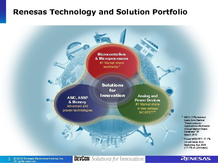 Renesas Technology and Solution Portfolio Microcontrollers & Microprocessors #1 Market share worldwide * ASIC, ASSP & Memory Advanced and proven technologies Solutions for Innovation Analog and Power Devices #1 Market share in low-voltage MOSFET** * MCU: 31% revenue basis from Gartner "Semiconductor Applications Worldwide Annual Market Share: Database" 25 March 2010 ** Power MOSFET: 17. 1% on unit basis from Marketing Eye 2009 (17. 1% on unit basis). 3 © 2010 Renesas Electronics America Inc. All rights reserved.
 Renesas Technology and Solution Portfolio Microcontrollers & Microprocessors #1 Market share worldwide * ASIC, ASSP & Memory Advanced and proven technologies Solutions for Innovation Analog and Power Devices #1 Market share in low-voltage MOSFET** * MCU: 31% revenue basis from Gartner "Semiconductor Applications Worldwide Annual Market Share: Database" 25 March 2010 ** Power MOSFET: 17. 1% on unit basis from Marketing Eye 2009 (17. 1% on unit basis). 4 © 2010 Renesas Electronics America Inc. All rights reserved.
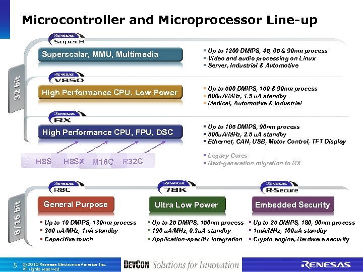 Microcontroller and Microprocessor Line-up Superscalar, MMU, Multimedia § Up to 1200 DMIPS, 45, 65 & 90 nm process § Video and audio processing on Linux § Server, Industrial & Automotive High Performance CPU, Low Power § Up to 500 DMIPS, 150 & 90 nm process § 600 u. A/MHz, 1. 5 u. A standby § Medical, Automotive & Industrial High Performance CPU, FPU, DSC H 8 SX M 16 C R 32 C General Purpose § Up to 10 DMIPS, 130 nm process § 350 u. A/MHz, 1 u. A standby § Capacitive touch 5 © 2010 Renesas Electronics America Inc. All rights reserved. § Up to 165 DMIPS, 90 nm process § 500 u. A/MHz, 2. 5 u. A standby § Ethernet, CAN, USB, Motor Control, TFT Display § Legacy Cores § Next-generation migration to RX Ultra Low Power Embedded Security § Up to 25 DMIPS, 150 nm process § Up to 25 DMIPS, 180, 90 nm process § 190 u. A/MHz, 0. 3 u. A standby § 1 m. A/MHz, 100 u. A standby § Application-specific integration § Crypto engine, Hardware security
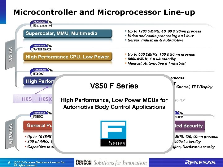 Microcontroller and Microprocessor Line-up Superscalar, MMU, Multimedia § Up to 1200 DMIPS, 45, 65 & 90 nm process § Video and audio processing on Linux § Server, Industrial & Automotive High Performance CPU, Low Power § Up to 500 DMIPS, 150 & 90 nm process § 600 u. A/MHz, 1. 5 u. A standby § Medical, Automotive & Industrial High Performance CPU, FPU, DSC § Up to 165 DMIPS, 90 nm process § 500 u. A/MHz, 2. 5 u. A standby § Ethernet, CAN, USB, Motor Control, TFT Display V 850 F Series H 8 S § Legacy Cores H 8 SX M 16 C Performance, Low Power MCUs for to RX § Next-generation migration High R 32 C Automotive Body Control Applications General Purpose § Up to 10 DMIPS, 130 nm process § 350 u. A/MHz, 1 u. A standby § Capacitive touch 6 © 2010 Renesas Electronics America Inc. All rights reserved. Ultra Low Power Embedded Security § Up to 25 DMIPS, 150 nm process § Up to 25 DMIPS, 180, 90 nm process § 190 u. A/MHz, 0. 3 u. A standby § 1 m. A/MHz, 100 u. A standby § Application-specific integration § Crypto engine, Hardware security
 Innovation in Automotive Lighting Technology 7 © 2010 Renesas Electronics America Inc. All rights reserved.
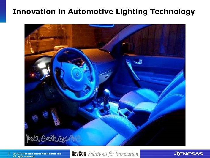
 Renesas’ F Series Enables Your Bright Ideas Renesas has developed an optimum, full system solution for vehicle lighting control. Renesas is providing you the means to implement your driver comfort and customization ideas in an easy and robust manner. 8 © 2010 Renesas Electronics America Inc. All rights reserved.
 Agenda n V 850/Fx 4 Product Introduction n Timer Array Unit (TAU) n PWM Delay & Driver Diagnostics n Conclusion 9 © 2010 Renesas Electronics America Inc. All rights reserved.
 Key Takeaways By the end of this session you will: n Understand the capabilities of the Timer Array Unit (TAU) n Understand the features and benefits of the PWM Delay Generator n Understand the features and benefits of the Driver Diagnostics Control Unit 10 © 2010 Renesas Electronics America Inc. All rights reserved.
 V 850/Fx 4 Product Introduction 11 © 2010 Renesas Electronics America Inc. All rights reserved.
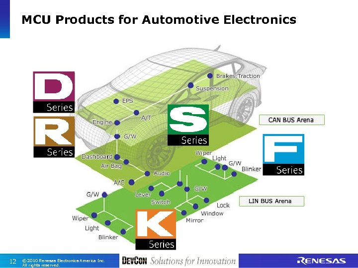 MCU Products for Automotive Electronics V 850/F Series 12 © 2010 Renesas Electronics America Inc. All rights reserved.
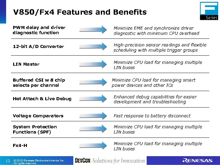 V 850/Fx 4 Features and Benefits PWM delay and driver diagnostic function Minimize EME and synchronize driver diagnostic with minimum CPU overhead 12 -bit A/D Converter High-precision sensor readings and flexible scheduling with multiple trigger groups LIN Master Minimize CPU load for managing multiple LIN buses Buffered CSI w 8 chip selects per channel Minimize CPU load for managing smart power devices and other ICs Hot Attach & Live Debug Voltage Comparators Fast response to battery disconnect System Protection Functions (SPF) Minimize CPU load for managing multiple LIN buses Fx 4 -H 13 Enhanced debug capabilities for easier development and troubleshooting Minimize CPU load for managing multiple LIN buses © 2010 Renesas Electronics America Inc. All rights reserved.
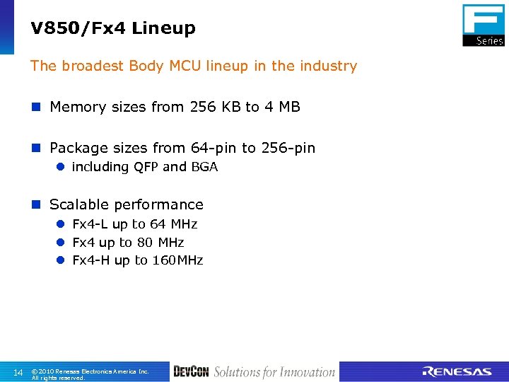 V 850/Fx 4 Lineup The broadest Body MCU lineup in the industry n Memory sizes from 256 KB to 4 MB n Package sizes from 64 -pin to 256 -pin l including QFP and BGA n Scalable performance l Fx 4 -L up to 64 MHz l Fx 4 up to 80 MHz l Fx 4 -H up to 160 MHz 14 © 2010 Renesas Electronics America Inc. All rights reserved.
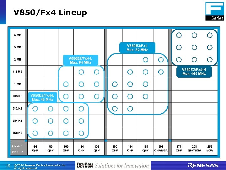 V 850/Fx 4 Lineup 15 © 2010 Renesas Electronics America Inc. All rights reserved.
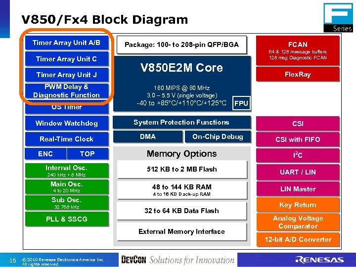 V 850/Fx 4 Block Diagram Timer Array Unit A/B Timer Array Unit C Timer Array Unit J PWM Delay & Diagnostic Function OS Timer Window Watchdog Real-Time Clock ENC TOP Internal Osc. 240 k. Hz + 8 MHz Main Osc. 4 to 20 MHz Sub Osc. 32. 768 k. Hz Package: 100 - to 208 -pin QFP/BGA FCAN 64 & 128 message buffers 128 msg Diagnostic FCAN V 850 E 2 M Core Flex. Ray 160 MIPS @ 80 MHz 3. 0 – 5. 5 V (single voltage) -40 to +85°C/+110°C/+125°C FPU System Protection Functions DMA On-Chip Debug CSI with FIFO Memory Options I 2 C 512 KB to 2 MB Flash UART / LIN 48 to 144 KB RAM LIN Master 4 to 16 KB Back-up RAM 32 to 64 KB Data Flash PLL & SSCG External Memory Interface Key Return Analog Voltage Comparator 12 -bit A/D Converter 16 © 2010 Renesas Electronics America Inc. All rights reserved.
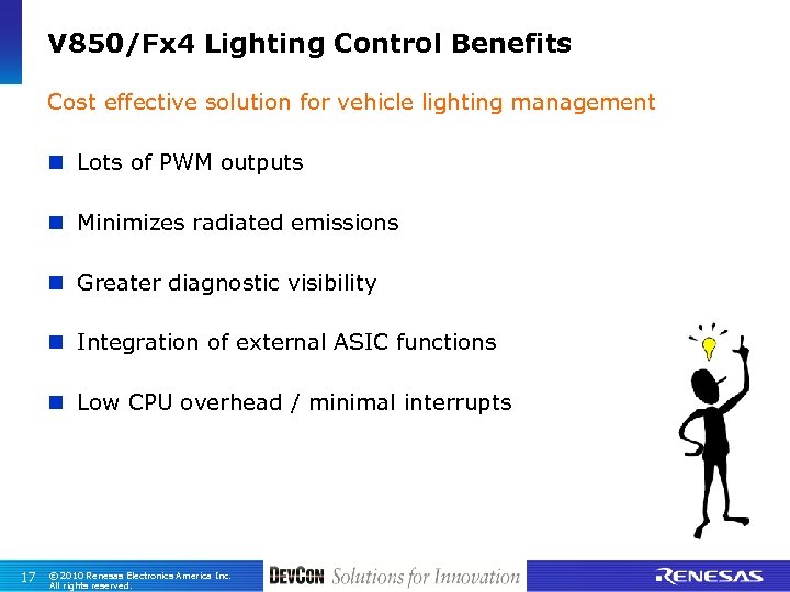 V 850/Fx 4 Lighting Control Benefits Cost effective solution for vehicle lighting management n Lots of PWM outputs n Minimizes radiated emissions n Greater diagnostic visibility n Integration of external ASIC functions n Low CPU overhead / minimal interrupts 17 © 2010 Renesas Electronics America Inc. All rights reserved.
 Timers in Automotive 18 © 2010 Renesas Electronics America Inc. All rights reserved.
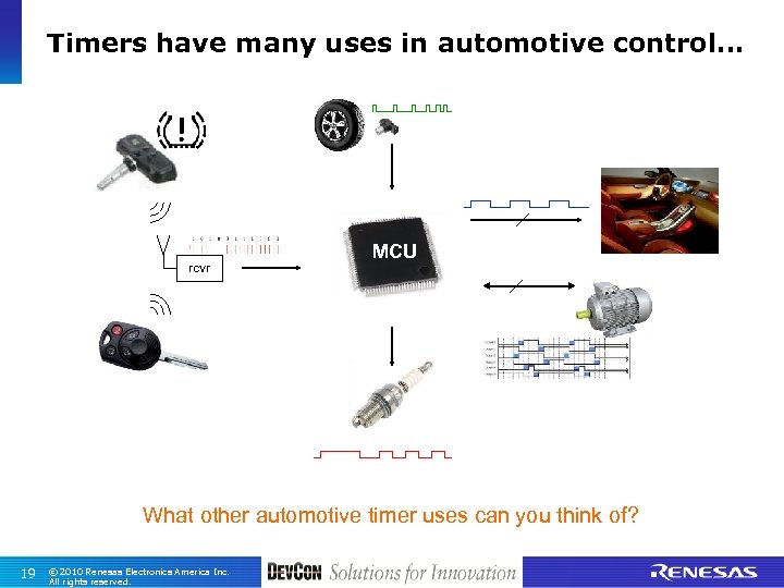 Timers have many uses in automotive control… rcvr MCU What other automotive timer uses can you think of? 19 © 2010 Renesas Electronics America Inc. All rights reserved.
 Timer Array Unit (TAU) 20 © 2010 Renesas Electronics America Inc. All rights reserved.
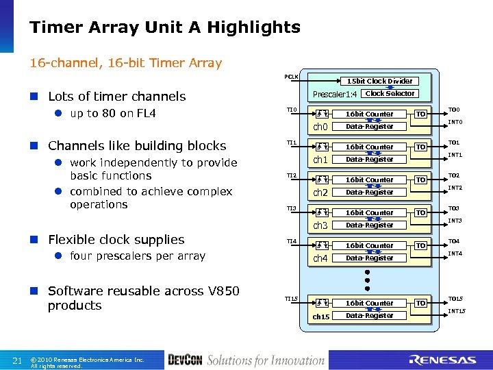 Timer Array Unit A Highlights 16 -channel, 16 -bit Timer Array PCLK n Lots of timer channels l up to 80 on FL 4 15 bit Clock Divider Prescaler 1: 4 TI 0 16 bit Counter ch 0 n Channels like building blocks l work independently to provide basic functions l combined to achieve complex operations TI 1 ch 1 TI 2 TI 3 TI 4 l four prescalers per array n Software reusable across V 850 products TI 15 ch 15 21 © 2010 Renesas Electronics America Inc. All rights reserved. TO Data-Register TO 2 INT 2 TO TO 3 INT 3 TO TO 4 INT 4 Data-Register 16 bit Counter TO 1 INT 1 Data-Register 16 bit Counter ch 4 TO Data-Register 16 bit Counter TO 0 INT 0 Data-Register 16 bit Counter ch 2 TO Data-Register 16 bit Counter ch 3 n Flexible clock supplies Clock Selector TO TO 15 INT 15
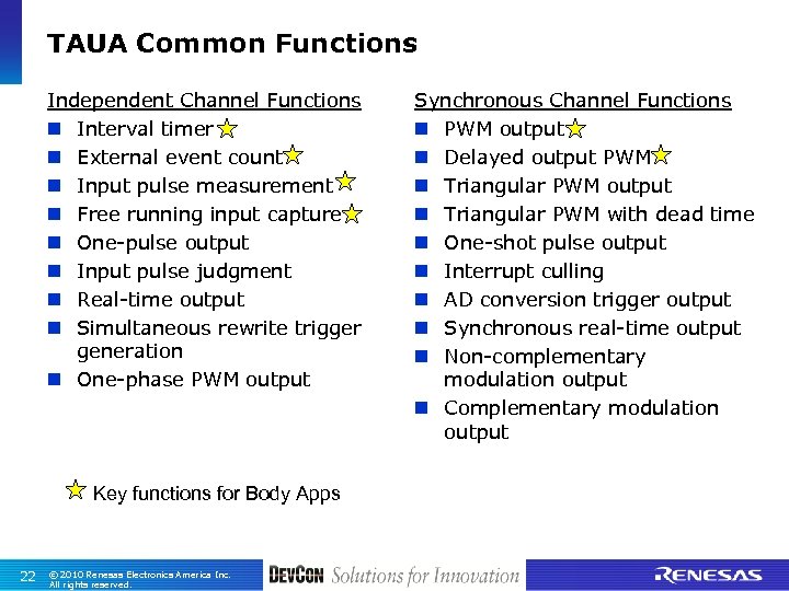 TAUA Common Functions Independent Channel Functions n Interval timer n External event count n Input pulse measurement n Free running input capture n One-pulse output n Input pulse judgment n Real-time output n Simultaneous rewrite trigger generation n One-phase PWM output Key functions for Body Apps 22 © 2010 Renesas Electronics America Inc. All rights reserved. Synchronous Channel Functions n PWM output n Delayed output PWM n Triangular PWM output n Triangular PWM with dead time n One-shot pulse output n Interrupt culling n AD conversion trigger output n Synchronous real-time output n Non-complementary modulation output n Complementary modulation output
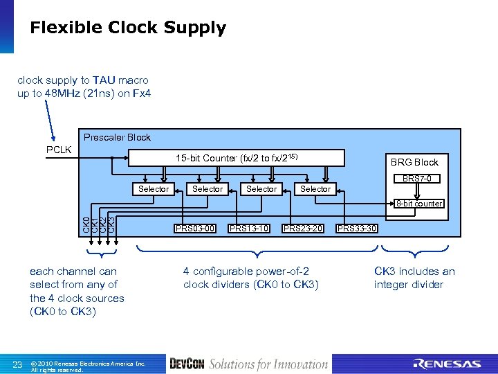 Flexible Clock Supply clock supply to TAU macro up to 48 MHz (21 ns) on Fx 4 Prescaler Block PCLK 15 -bit Counter (fx/2 to fx/215) BRG Block BRS 7 -0 Selector CK 0 CK 1 CK 2 CK 3 8 -bit counter each channel can select from any of the 4 clock sources (CK 0 to CK 3) 23 © 2010 Renesas Electronics America Inc. All rights reserved. PRS 03 -00 PRS 13 -10 PRS 23 -20 4 configurable power-of-2 clock dividers (CK 0 to CK 3) PRS 33 -30 CK 3 includes an integer divider
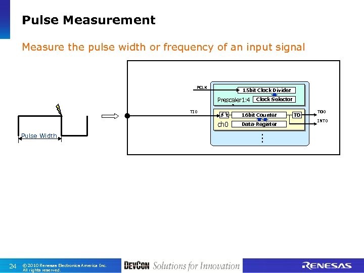 Pulse Measurement Measure the pulse width or frequency of an input signal PCLK 15 bit Clock Divider Prescaler 1: 4 ` TI 0 ch 0 Pulse Width 24 © 2010 Renesas Electronics America Inc. All rights reserved. Clock Selector 16 bit Counter Data-Register . . . TO TO 0 INT 0
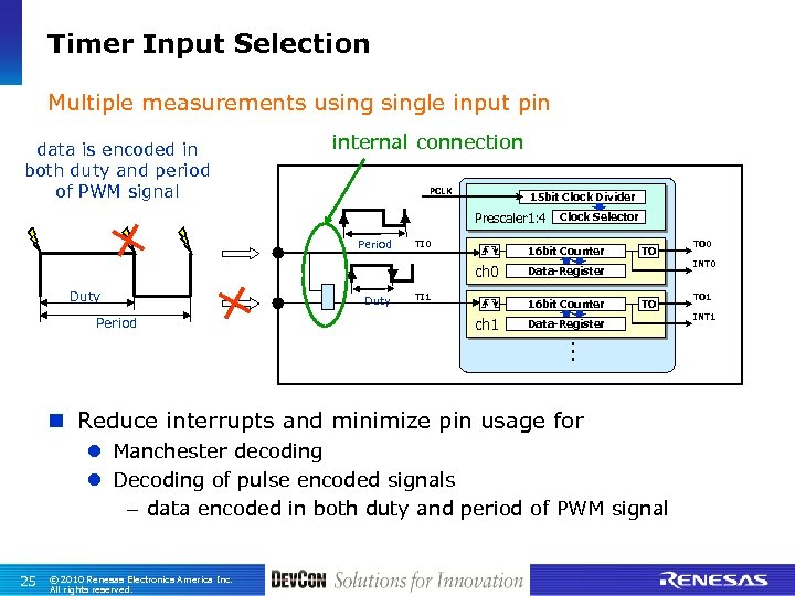 Timer Input Selection Multiple measurements usingle input pin data is encoded in both duty and period of PWM signal internal connection PCLK 15 bit Clock Divider Prescaler 1: 4 Period TI 0 16 bit Counter ch 0 Duty Period Duty Clock Selector TI 1 ` TO Data-Register . . . n Reduce interrupts and minimize pin usage for l Manchester decoding l Decoding of pulse encoded signals – data encoded in both duty and period of PWM signal 25 © 2010 Renesas Electronics America Inc. All rights reserved. TO 0 INT 0 Data-Register 16 bit Counter ch 1 TO TO 1 INT 1
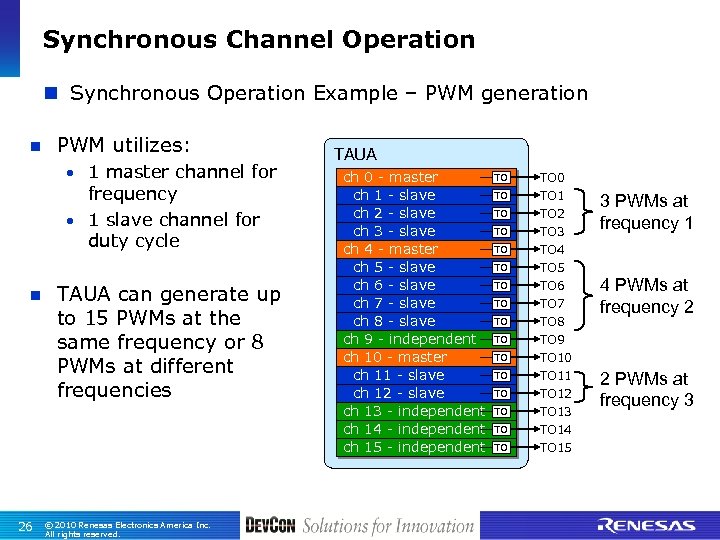 Synchronous Channel Operation n Synchronous Operation Example – PWM generation n PWM utilizes: • 1 master channel for frequency • 1 slave channel for duty cycle n 26 TAUA can generate up to 15 PWMs at the same frequency or 8 PWMs at different frequencies © 2010 Renesas Electronics America Inc. All rights reserved. TAUA ch 0 - master ch 1 1 - slave ch ch 2 2 - slave ch ch 3 3 - slave ch ch 4 4 - slave ch - master ch 5 5 - slave ch ch 6 6 - slave ch ch 7 7 - slave ch ch 8 8 - slave ch ch - independent ch 9 9 - slave ch 10 - - slave ch 10 master ch 11 - slave ch 11 ch 12 - slave ch 12 ch 13 - - slave ch 13 independent ch 14 - - slave ch 14 master independent ch 15 - - slave ch 15 independent TO TO TO TO TO 0 TO 1 TO 2 TO 3 TO 4 TO 5 TO 6 TO 7 TO 8 TO 9 TO 10 TO 11 TO 12 TO 13 TO 14 TO 15 3 PWMs at frequency 1 4 PWMs at 5 PWMs at 15 PWMs frequency 2 at the same frequency 2 PWMs at 3 PWMs at frequency 3 1 PWMs at frequency 4
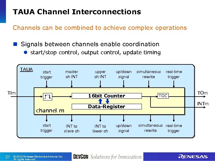 TAUA Channel Interconnections Channels can be combined to achieve complex operations n Signals between channels enable coordination l start/stop control, output control, update timing TAUA master ch INT start trigger TI TIm channel m start trigger 27 © 2010 Renesas Electronics America Inc. All rights reserved. INT to slave ch upper ch INT up/down signal 16 bit Counter simultaneous rewrite real-time trigger TOC INTm Data-Register INT to lower ch up/down signal TOm simultaneous real-time rewrite trigger
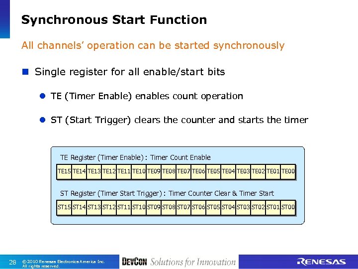 Synchronous Start Function All channels’ operation can be started synchronously n Single register for all enable/start bits l TE (Timer Enable) enables count operation l ST (Start Trigger) clears the counter and starts the timer TE Register (Timer Enable) : Timer Count Enable TE 15 TE 14 TE 13 TE 12 TE 11 TE 10 TE 09 TE 08 TE 07 TE 06 TE 05 TE 04 TE 03 TE 02 TE 01 TE 00 ST Register (Timer Start Trigger) : Timer Counter Clear & Timer Start ST 15 ST 14 ST 13 ST 12 ST 11 ST 10 ST 09 ST 08 ST 07 ST 06 ST 05 ST 04 ST 03 ST 02 ST 01 ST 00 28 © 2010 Renesas Electronics America Inc. All rights reserved.
 Simultaneous Rewrite n Synchronously update multiple channels l compare/start values l output logic n Update becomes active upon user selectable event l master channel l upper channel l interrupt from upper channel n Example Application: 3 phase motor control l simultaneous update to the duty values of all phases 29 © 2010 Renesas Electronics America Inc. All rights reserved.
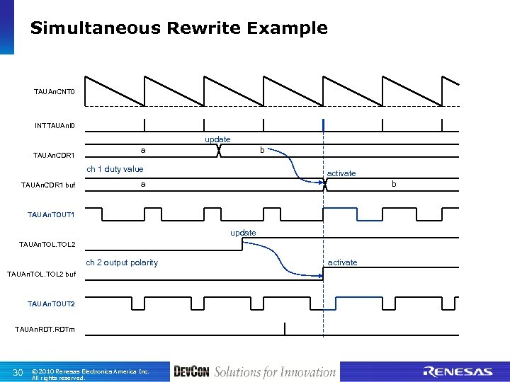 Simultaneous Rewrite Example TAUAn. CNT 0 INTTAUAn. I 0 update TAUAn. CDR 1 a b ch 1 duty value TAUAn. CDR 1 buf activate a b TAUAn. TOUT 1 update TAUAn. TOL 2 ch 2 output polarity TAUAn. TOL 2 buf TAUAn. TOUT 2 TAUAn. RDTm 30 © 2010 Renesas Electronics America Inc. All rights reserved. activate
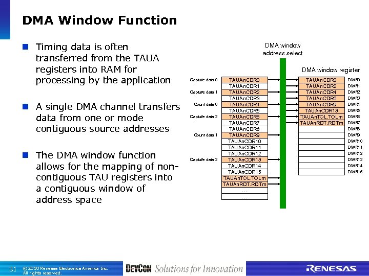 DMA Window Function n Timing data is often transferred from the TAUA registers into RAM for processing by the application DMA window address select DMA window register Capture data 0 Capture data 1 n A single DMA channel transfers data from one or mode contiguous source addresses n The DMA window function allows for the mapping of noncontiguous TAU registers into a contiguous window of address space 31 © 2010 Renesas Electronics America Inc. All rights reserved. Count data 0 Capture data 2 Count data 1 Capture data 3 TAUAn. CDR 0 TAUAn. CDR 1 TAUAn. CDR 2 TAUAn. CDR 3 TAUAn. CDR 4 TAUAn. CDR 5 TAUAn. CDR 6 TAUAn. CDR 7 TAUAn. CDR 8 TAUAn. CDR 9 TAUAn. CDR 10 TAUAn. CDR 11 TAUAn. CDR 12 TAUAn. CDR 13 TAUAn. CDR 14 TAUAn. CDR 15 TAUAn. TOLm TAUAn. RDTm … … TAUAn. CDR 0 TAUAn. CDR 2 TAUAn. CDR 4 TAUAn. CDR 6 TAUAn. CDR 9 TAUAn. CDR 13 TAUAn. TOLm TAUAn. RDTm DWR 0 DWR 1 DWR 2 DWR 3 DWR 4 DWR 5 DWR 6 DWR 7 DWR 8 DWR 9 DWR 10 DWR 11 DWR 12 DWR 13 DWR 14 DWR 15
 Timer Array Unit Derivatives 32 © 2010 Renesas Electronics America Inc. All rights reserved.
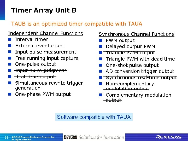 Timer Array Unit B TAUB is an optimized timer compatible with TAUA Independent Channel Functions n Interval timer n External event count n Input pulse measurement n Free running input capture n One-pulse output n Input pulse judgment n Real-time output n Simultaneous rewrite trigger generation n One-phase PWM output Synchronous Channel Functions n PWM output n Delayed output PWM n Triangle PWM output n Triangle PWM with dead time n One-shot pulse output n AD conversion trigger output n Synchronous real-time output n Non-complementary modulation output n Complementary modulation output Software compatible with TAUA 33 © 2010 Renesas Electronics America Inc. All rights reserved.
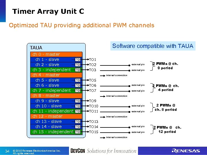 Timer Array Unit C Optimized TAU providing additional PWM channels Software compatible with TAUA ch 0 - master ch 1 - slave ch 2 - slave ch 3 - independent ch 4 - master ch 5 - slave ch 6 - slave ch 7 - independent ch 8 - master ch 9 - slave ch 10 - slave ch 11 - independent ch 12 - master ch 13 - slave ch 14 - slave ch 15 - independent TO TO 1 TO 2 TO 3 external pin internal connection TO TO 5 TO 6 TO 7 external pin © 2010 Renesas Electronics America Inc. All rights reserved. 2 PWMs @ ch. 4 period internal connection TO TO 9 TO 10 TO 11 external pin 2 PWMs @ ch. 8 period internal connection TO TO 13 TO 14 external pin TO TO 15 external pin TO internal connection 34 2 PWMs @ ch. 0 period 2 PWMs @ ch. 12 period
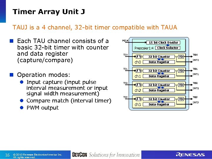 Timer Array Unit J TAUJ is a 4 channel, 32 -bit timer compatible with TAUA n Each TAU channel consists of a basic 32 -bit timer with counter and data register (capture/compare) PCLK 15 bit Clock Divider Prescaler 1: 4 TI 0 32 bit Counter ch 0 TI 1 n Operation modes: l Input capture (input pulse interval measurement or input signal width measurement) l Compare match (interval timer) l PWM output 35 © 2010 Renesas Electronics America Inc. All rights reserved. Clock Selector TI 2 ch 2 TI 3 Data-Register TO 1 INT 1 TO TO 2 INT 2 Data-Register 32 bit Counter ch 3 TO Data-Register 32 bit Counter TO 0 INT 0 Data-Register 32 bit Counter ch 1 TO TO TO 3 INT 3
 Review Question How many PWM outputs does TAUC generate? n TAUC generates up to 8 PWM with 4 independent frequencies n TAUA/B generates 15 PWM with a common frequency or up to 8 PWM with independent frequencies 36 © 2010 Renesas Electronics America Inc. All rights reserved.
 PWM Delay & Driver Diagnostics 37 © 2010 Renesas Electronics America Inc. All rights reserved.
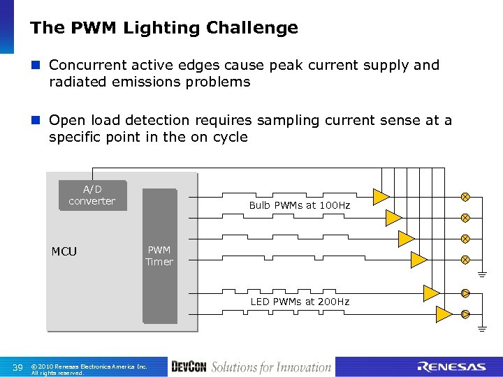 The PWM Lighting Challenge n Concurrent active edges cause peak current supply and radiated emissions problems n Open load detection requires sampling current sense at a specific point in the on cycle A/D converter MCU Bulb PWMs at 100 Hz PWM Timer LED PWMs at 200 Hz 39 © 2010 Renesas Electronics America Inc. All rights reserved.
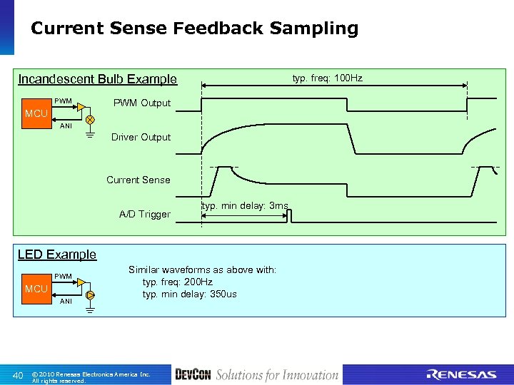 Current Sense Feedback Sampling Incandescent Bulb Example PWM MCU typ. freq: 100 Hz PWM Output ANI Driver Output Current Sense A/D Trigger typ. min delay: 3 ms LED Example PWM MCU ANI 40 Similar waveforms as above with: typ. freq: 200 Hz typ. min delay: 350 us © 2010 Renesas Electronics America Inc. All rights reserved.
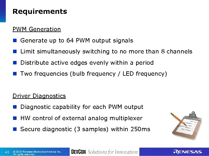 Requirements PWM Generation n Generate up to 64 PWM output signals n Limit simultaneously switching to no more than 8 channels n Distribute active edges evenly within a period n Two frequencies (bulb frequency / LED frequency) Driver Diagnostics n Diagnostic capability for each PWM output n HW control of external analog multiplexer n Secure diagnostic (3 samples) within 250 ms 41 © 2010 Renesas Electronics America Inc. All rights reserved.
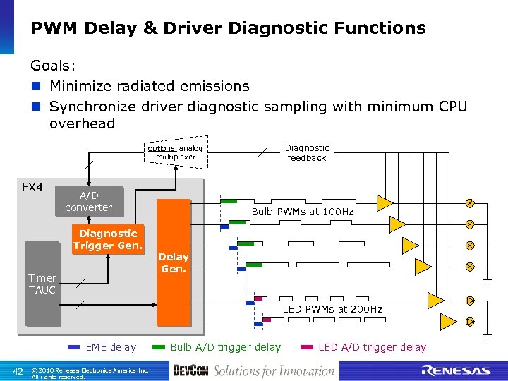 PWM Delay & Driver Diagnostic Functions Goals: n Minimize radiated emissions n Synchronize driver diagnostic sampling with minimum CPU overhead Diagnostic feedback optional analog multiplexer FX 4 A/D converter Diagnostic Trigger Gen. Timer TAUC Bulb PWMs at 100 Hz Delay Gen. LED PWMs at 200 Hz EME delay 42 © 2010 Renesas Electronics America Inc. All rights reserved. Bulb A/D trigger delay LED A/D trigger delay
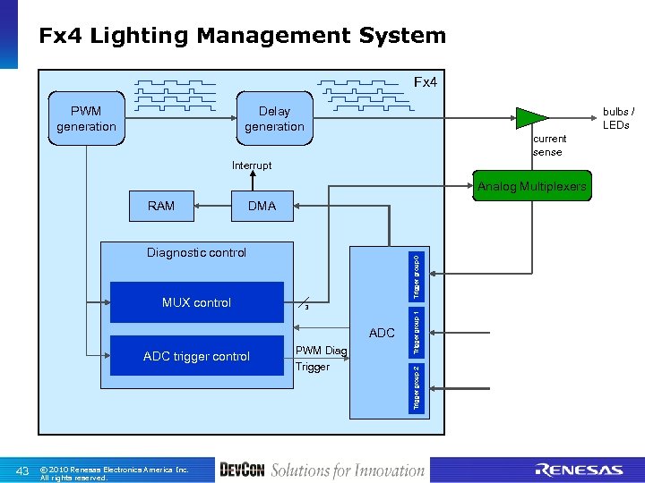 Fx 4 Lighting Management System Fx 4 PWM generation Delay generation bulbs / LEDs current sense Interrupt Analog Multiplexers DMA 3 ADC trigger control 43 © 2010 Renesas Electronics America Inc. All rights reserved. PWM Diag Trigger group 1 MUX control Trigger group 0 Diagnostic control Trigger group 2 RAM
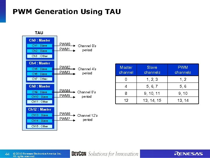 PWM Generation Using TAU Ch 0 : Master Ch 1 : Slave Ch 2 : Slave Ch 3 : Other PWM 0 PWM 1 Channel 0’s period PWM 2 PWM 3 Channel 4’s period Ch 4 : Master Ch 5 : Slave Ch 6 : Slave Ch 7 : Other Ch 7 Ch 9 : Slave Ch 10 Ch 11 : Other Ch 11 PWM 4 PWM 5 Ch 12 : Master Ch 13 : Slave Ch 13 Ch 14 : Slave Ch 14 PWM 6 PWM 7 Ch 15 : Other Ch 15 44 © 2010 Renesas Electronics America Inc. All rights reserved. Channel 12’s period PWM channels 1, 2, 3 1, 2 4 Channel 8’s period Slave channels 0 Ch 8 : Master channel 5, 6, 7 5, 6 8 9, 10, 11 9, 10 12 13, 14, 15 13, 14
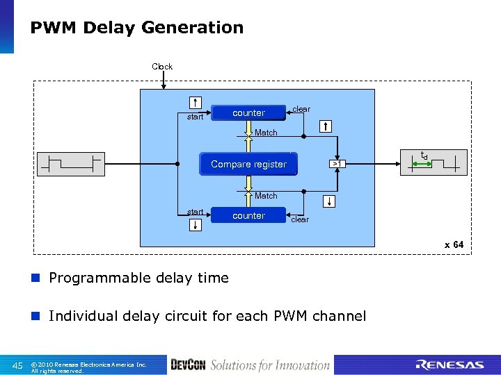 PWM Delay Generation Clock counter start clear Match Compare register >1 td Match start counter clear x 64 n Programmable delay time n Individual delay circuit for each PWM channel 45 © 2010 Renesas Electronics America Inc. All rights reserved.
 PWM Frequency Definitions n Synchronous: PWM outputs with a frequency that is an integer multiple of a base PWM frequency (fbase) n Asynchronous: PWM outputs with a frequency that is not an integer multiple of the base PWM frequency n For synchronous PWMs, exactly 46 © 2010 Renesas Electronics America Inc. All rights reserved.
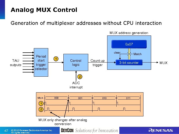 Analog MUX Control Generation of multiplexer addresses without CPU interaction MUX address generation 0 x 07 clear TAU outputs Period start trigger selector 1 Control logic Count up trigger Match 3 -bit counter 2 ADC interrupt MUX 000 001 1 2 MUX only changes after analog conversion 47 © 2010 Renesas Electronics America Inc. All rights reserved. 010 011 MUX
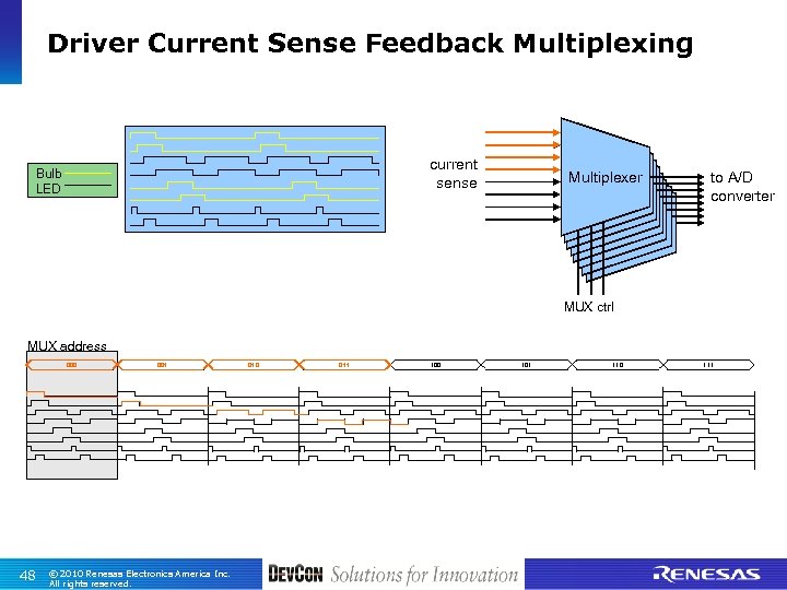 Driver Current Sense Feedback Multiplexing current sense Bulb LED Multiplexer Multiplexer to A/D converter MUX ctrl MUX address 000 48 001 © 2010 Renesas Electronics America Inc. All rights reserved. 010 011 100 101 110 111
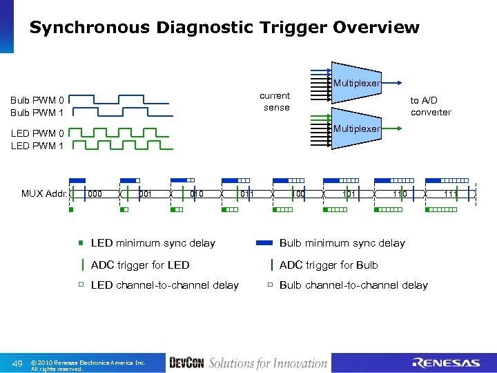 Synchronous Diagnostic Trigger Overview Multiplexer current sense Bulb PWM 0 Bulb PWM 1 to A/D converter Multiplexer LED PWM 0 LED PWM 1 MUX Addr. 000 001 010 011 100 101 110 LED minimum sync delay ADC trigger for LED ADC trigger for Bulb LED channel-to-channel delay 49 Bulb minimum sync delay Bulb channel-to-channel delay © 2010 Renesas Electronics America Inc. All rights reserved. 111
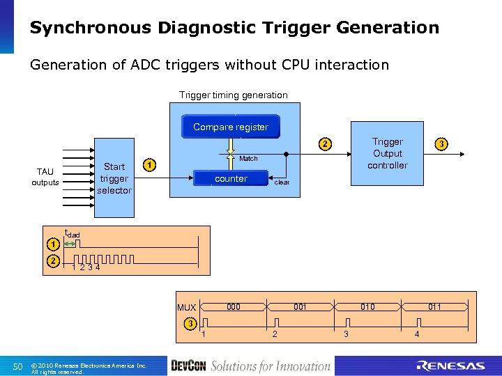 Synchronous Diagnostic Trigger Generation of ADC triggers without CPU interaction Trigger timing generation Compare register Trigger Output controller 2 Start trigger selector TAU outputs Match 1 counter 3 clear td. ad 1 2 1234 000 MUX 001 010 011 3 1 50 © 2010 Renesas Electronics America Inc. All rights reserved. 2 3 4
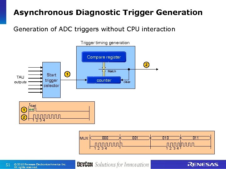 Asynchronous Diagnostic Trigger Generation of ADC triggers without CPU interaction Trigger timing generation Compare register 2 Start trigger selector TAU outputs Match 1 counter clear td. ad 1 2 1234 MUX 000 1234 51 © 2010 Renesas Electronics America Inc. All rights reserved. 001 010 1234 011
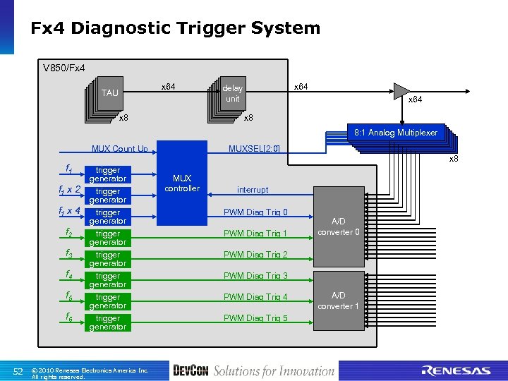 Fx 4 Diagnostic Trigger System V 850/Fx 4 x 64 TAU x 8 x 64 delay unit x 64 x 8 8: 1 Analog Multiplexer MUX Count Up MUXSEL[2: 0] x 8 f 1 x 2 trigger generator f 1 x 4 trigger generator PWM Diag Trig 0 f 2 trigger generator PWM Diag Trig 1 f 3 trigger generator PWM Diag Trig 2 f 4 trigger generator PWM Diag Trig 3 f 5 trigger generator PWM Diag Trig 4 f 6 52 trigger generator PWM Diag Trig 5 © 2010 Renesas Electronics America Inc. All rights reserved. MUX controller interrupt A/D converter 0 A/D converter 1
 Driver Diagnostics Software n Transfer of ADC conversion results to RAM by DMA n Single interrupt after availabilty of diagnostic value from all PWM channels n Evaluation of diagnostic values in ISR after 8 bulb periods 53 © 2010 Renesas Electronics America Inc. All rights reserved.
 Review Questions 1. What benefit does the staggered delay of PWM outputs provide? 2. Can anyone explain the difference between the synchronous and asynchronous A/D triggers generated by the Driver Diagnostics Control Unit? 54 © 2010 Renesas Electronics America Inc. All rights reserved.
 Requirements Review PWM Generation n Generate up to 64 PWM channels R Support for up to 64 PWM channels on FL 4 n Limit simultaneously switching to no more than 8 channels R Individual delay setting for each channel n Distribute active edges evenly within a period R Individual delay setting for each channel n Two frequencies (bulb frequency / LED frequency) R 3 synchronous frequencies + 2 independent frequencies possible 55 © 2010 Renesas Electronics America Inc. All rights reserved.
 Requirements Review Driver Diagnostics n Diagnostic capability for each PWM output R Support for up to 64 synchronous and asynchronous PWM channels on FL 4 n HW control of external analog multiplexer R Fully automatic multiplexer control in HW n Secure diagnostic (3 samples) within 250 ms R For 100 Hz signal, 3 conversions of all 64 channels within 240 ms 56 © 2010 Renesas Electronics America Inc. All rights reserved.
 Review Question Can anyone name some of the benefits that Fx 4 provides for lighting management? n Lots of PWM outputs n Minimizes radiated emissions n Greater diagnostic visibility n Integration of external ASIC functions n Low CPU overhead / minimal interrupts 57 © 2010 Renesas Electronics America Inc. All rights reserved.
 Renesas’ F Series Enables Your Bright Ideas 58 © 2010 Renesas Electronics America Inc. All rights reserved.
 Questions? 59 © 2010 Renesas Electronics America Inc. All rights reserved.
 Renesas Electronics America Inc.


