ab50989f60dd491ecc9a00fcf8d3e41b.ppt
- Количество слайдов: 95
 Homework/Test questions Name: 1. Read the lecture on nanotechnology by R. P. Feynmann, "There's Plenty of Room at the Bottom": http: //www. zyvex. com/nanotech/feynman. html Provide Answers: What does he mean by shadow it by evaporating gold at an angle. Hand draw a picture. What did he propose to make copies of the master? Hand draw a picture of what you understand he suggested.
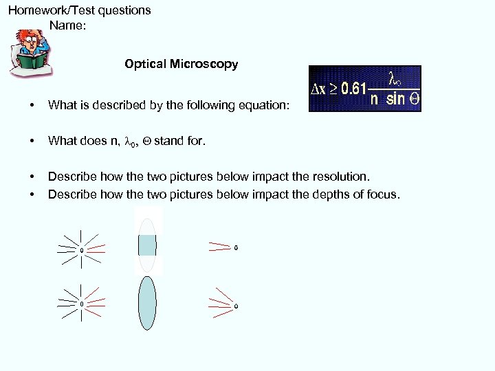 Homework/Test questions Name: Optical Microscopy • What is described by the following equation: • What does n, l 0, Q stand for. • • Describe how the two pictures below impact the resolution. Describe how the two pictures below impact the depths of focus.
 Homework/Test questions Name: • what are the elements of an SEM? • how does the electron gun work? • what is the acceleration voltage? • what happens if electron impact on the surface? • what signals can you record and where would you place the detector? • What is the primary reason which limits the resolution of an SEM? • Name three different signals that you can record, the primary application of the three signals, and the anticipated resolution in each case.
 Homework/Test questions Name: Consider three signals Elastically Scattered Secondary X rays Where do you place the detector and how effective is the use of an external bias?
 Homework/Test questions Name: • Draw the process of Auger electron emission? Sea of valence electrons L 23 2 s L 1 K K 1 s electron vacancy • L 23 2 s K 1 s K 2 p Sea of valence electrons 2 s L 1 K 1 s K 2 p electron vacancy Describe the process: initial state step 1: step 2:
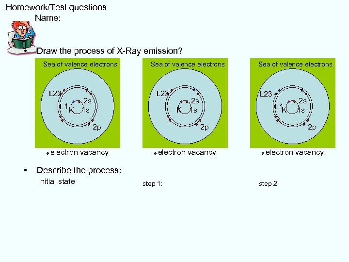 Homework/Test questions Name: • Draw the process of X-Ray emission? Sea of valence electrons L 23 2 s L 1 K K 1 s electron vacancy • L 23 2 s K 1 s K 2 p Sea of valence electrons 2 s L 1 K 1 s K 2 p electron vacancy Describe the process: initial state step 1: step 2:
 Homework/Test questions Name: • Draw the process of Auger electron emission, what is the energy in e. V? • Draw the process of X-Ray emission what is the energy in e. V? • Label the axis of an EDS spectra. • What is an ionizing process?
 Homework/Test questions Name: • Label the axis of an EDS spectra. • What is an ionizing process?
 Homework/Test questions Name: • Following a K shell excitation, the energies of the emitted characteristic X-ray and the equivalent emitted Auger electron are slightly different. Complete the equation: • Exray = ( EK - ) • Eauger = ( EK )
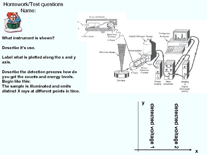 Homework/Test questions Name: What instrument is shown? Describe it’s use. Label what is plotted along the x and y axis. Describe the detection process how do you get the counts and energy levels. Begin like this: The sample is illuminated and emits distinct X rays at different points in time. detected voltage 2 detected voltage 1 y x
 Homework/Test questions Name: Name two scanning probe instruments. Select one and draw the basic elements that form the system. Label all the necessary physical modules and parts that are involved in the feedback loop.
 Homework/Test questions Name: What you should know? Test Questions: Select one -- an AFM or STM and draw the basic elements that form the system. Label all the necessary physical modules and parts that are involved in the feedback loop. Describe in you own words how the feedback loop works if the instruments scans over the surface and encounters a positive step in the topography. Begin with the cause: A positive step height will increase/decrease the xxx. The xxx will. . . yyy. The yyy will. . . zzz. The zzz will. . . mmm. The mmm will. .
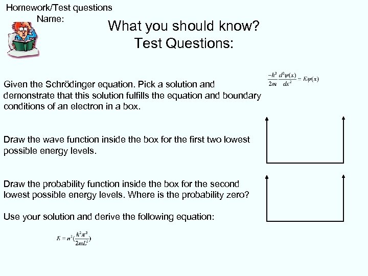 Homework/Test questions Name: What you should know? Test Questions: Given the Schrödinger equation. Pick a solution and demonstrate that this solution fulfills the equation and boundary conditions of an electron in a box. Draw the wave function inside the box for the first two lowest possible energy levels. Draw the probability function inside the box for the second lowest possible energy levels. Where is the probability zero? Use your solution and derive the following equation:
 Homework/Test questions Name: For tunneling to occur - (A) the wavefunctions of both surfaces have to be complementary, (B) the wavefunctions of both surfaces have to overlap (C) the wavefunctions of both surfaces have to be complex (D) the surface require a small workfunction (E) the surface require a large workfunction (F) a larger workfunction requires a smaller separation for tunneling to occur. (F) a larger workfunction requires a larger separation for tunneling to occur.
 Homework/Test questions Name: • Write down an equation that describes how the tunneling current between two metal surfaces depends on the distance between two surfaces. I = Io *. . • There is a characteristic unit K how big is this typically for most materials: (A) K=1/(. 1 nm) , (B) 1/(10 nm), (C)1/(1000 nm)? • If you increase the distance by a factor of 10, derive an equation that tells you how big a change in the current you will get considering tunneling?
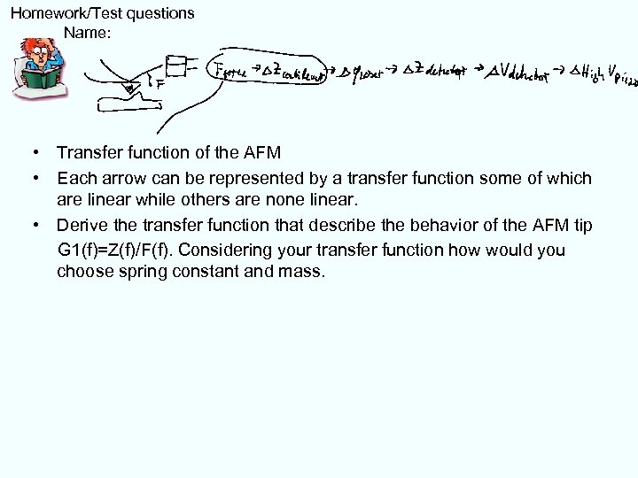 Homework/Test questions Name: • Transfer function of the AFM • Each arrow can be represented by a transfer function some of which are linear while others are none linear. • Derive the transfer function that describe the behavior of the AFM tip G 1(f)=Z(f)/F(f). Considering your transfer function how would you choose spring constant and mass.
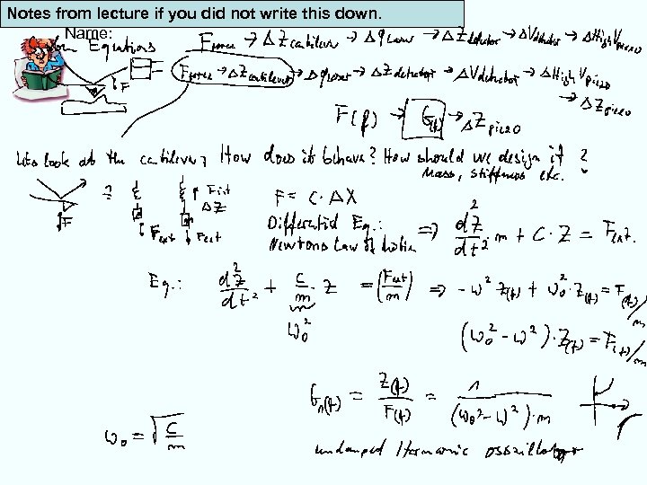 Homework/Test questions did not write this down. Notes from lecture if you Name:
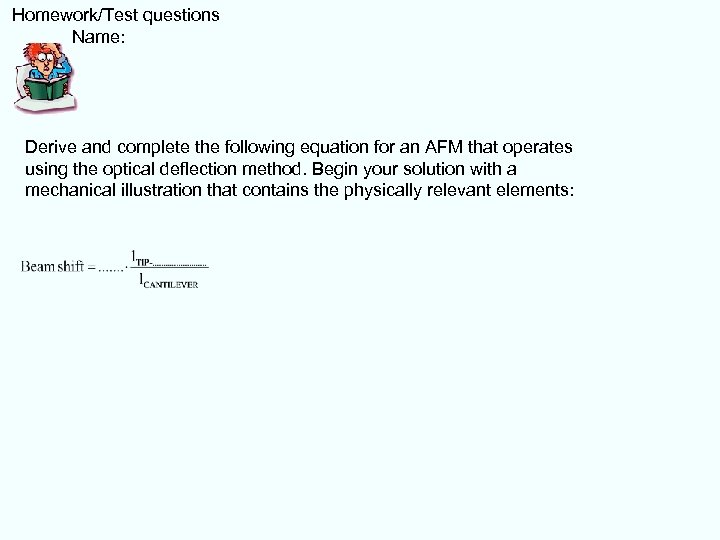 Homework/Test questions Name: Derive and complete the following equation for an AFM that operates using the optical deflection method. Begin your solution with a mechanical illustration that contains the physically relevant elements:
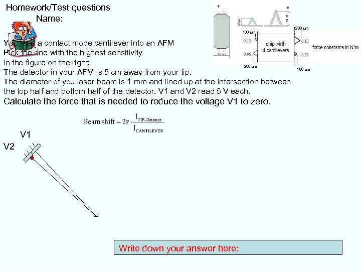 Homework/Test questions Name: 100 um You load a contact mode cantilever into an AFM Pick the one with the highest sensitivity in the figure on the right: 200 um The detector in your AFM is 5 cm away from your tip. The diameter of you laser beam is 1 mm and lined up at the intersection between the top half and bottom half of the detector. V 1 and V 2 read 5 V each. Calculate the force that is needed to reduce the voltage V 1 to zero. V 1 V 2 Write down your answer here: 200 um 100 um
 Homework/Test questions Name: • Write down 4 different forces that can be detected between an AFM tip and a substrate. The AFM tip has a tip radius of 20 nm. - (1). . . . - (2). . . . - (3). . . . - (4). . . . • Complete the sentence: With the exception of. . . these forces are typically in the . . . N (select: f. N, n. N, p. N, m. N) range. • In the force distance curves that we have taken one force did dominate. Which one? . . • Write down one equation that can be used to estimate a force.
 Homework/Test questions Name: • Describe the basic function of How and Atomic Force Microscope can be used to measure the Electric Surface Potential Distribution? Consider the concept of feedback. There is a need for a closed loop control system to get quantitative values of the surface potential. Draw and label the parts that are required including, mechanical, optical, and electrical elements to form the particular closed loop system whereby the output signal is the surface potential. Clearly label the location where you would monitor the surface potential.
 Homework/Test questions Name: • Draw a force distance curve that you would expect to record with an AFM in air at ambient pressure and humidity. • Label the axis • Label a regions where the total force is attractive. • Label a region where the total forces is repulsive. • Name two attractive = • and one repulsive force = • that you know. Added:
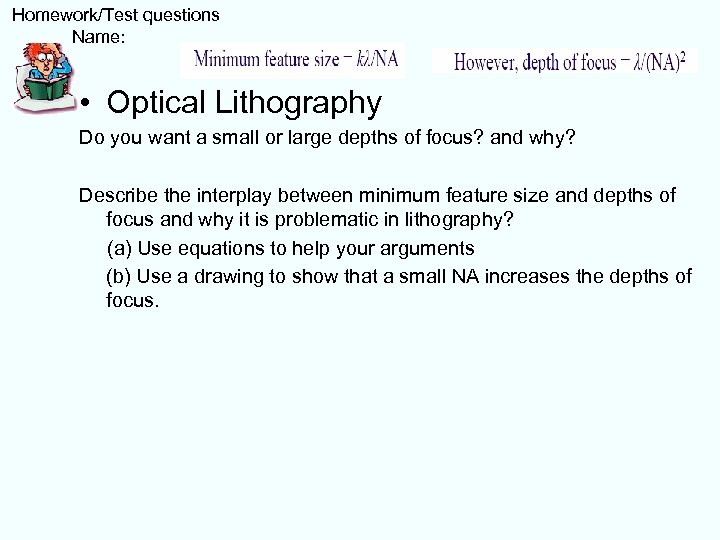 Homework/Test questions Name: • Optical Lithography Do you want a small or large depths of focus? and why? Describe the interplay between minimum feature size and depths of focus and why it is problematic in lithography? (a) Use equations to help your arguments (b) Use a drawing to show that a small NA increases the depths of focus.
 Homework/Test questions Name: Why is the resolution limited of an ebeam writer and not equal to half the wavelength of an electron? Which electron cause most damage (loose energy)? Backscattered or Secondary? What resolution do you expect? 10 nm, 100 nm, 1 um How could the film thickness effect the resolution?
 Homework/Test questions Name: • Name three top down Micro/Nanofabrication methods? • Write down what limits the resolution in each cases? • Write down the minimal line width that you expect? • Classify the throughput using parallel (fast) and serial (slow)? • Which once are available to small companies?
 Homework/Test questions Name: Optical Lithography • Deep UV Lithography in the 157 -193 nm range is challenging because the optics/lense is. . • Extreme UV requires the use of re………… optics.
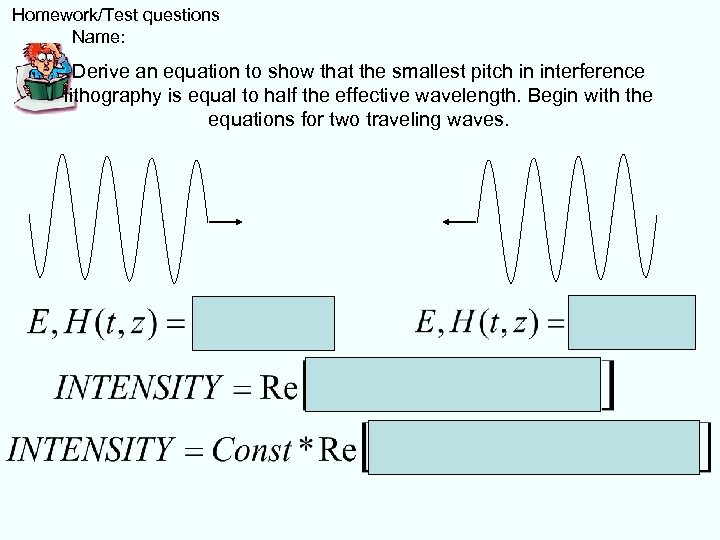 Homework/Test questions Name: Derive an equation to show that the smallest pitch in interference lithography is equal to half the effective wavelength. Begin with the equations for two traveling waves.
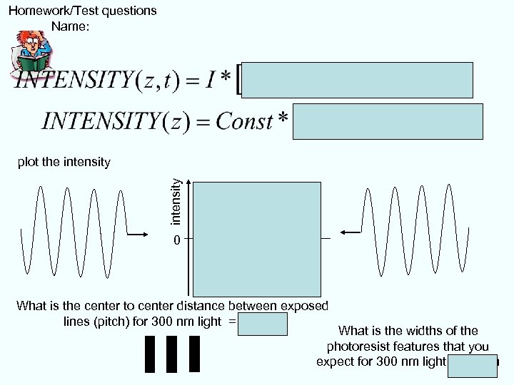 Homework/Test questions Name: intensity plot the intensity 0 What is the center to center distance between exposed lines (pitch) for 300 nm light = 150 nm What is the widths of the photoresist features that you expect for 300 nm light ~70 nm
 Homework/Test questions Name: Spin coating • What do you think controls the film thickness? - spin speed connected - viscosity of the solution - and solvent to polymer mass ratio • What could you do to increase thickness of the spin-coated layer 10 times?
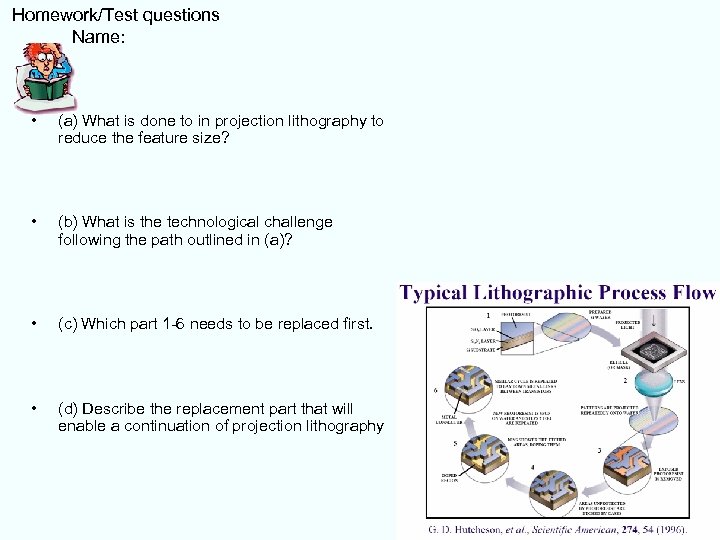 Homework/Test questions Name: • (a) What is done to in projection lithography to reduce the feature size? • (b) What is the technological challenge following the path outlined in (a)? • (c) Which part 1 -6 needs to be replaced first. • (d) Describe the replacement part that will enable a continuation of projection lithography
 Homework/Test questions Name: Vacuum deposition • Describe why deposition rate is a function of pressure? Find a gas kinetic equation to justify your arguments.
 Homework/Test questions Name: added: • Why is the deposition rate slow and control large when you go to high vacuum systems. • Write down an equation that relates the volume number concentration with the pressure.
 Homework/Test questions Name: • Given is a vacuum system that you evacuated to 10^-7 Torr. • After heating a gold pellet the pressure increases to 10^-6 Torr where it stabilizes. • Estimate the Au atom volume concentration. n = 3. 3 1016 /m 3 • What is the average spacing between the gold atoms? spacing = 3. 1 um e=1. 6 10 -19 C 750 Torr = 0. 98 atm = 1 bar = 105 Pa = 105 N/m²
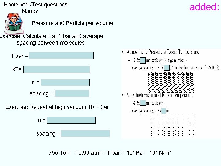 Homework/Test questions Name: Pressure and Particle per volume Exercise: Calculate n at 1 bar and average spacing between molecules 1 bar = 105 Pa = 105 N/m² = n k. T= 25 me. V=25 m. V*1. 6 10 -19 C n = 2. 5 1025 /m 3 spacing = 3. 4 nm Exercise: Repeat at high vacuum 10 -12 bar n = 2. 5 1013 /m 3 spacing = 30 um 750 Torr = 0. 98 atm = 1 bar = 105 Pa = 105 N/m² added:
 Homework/Test questions Name: • What is the equilibrium vapor pressure of silver at 1200 deg. C? • Under equilibrium pressure of silver at 1200 deg. C what is the volume number concentration in 1 m 3 and the combined weigth of all the atoms in this volume in nano grams? x ng
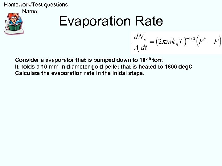 Homework/Test questions Name: Evaporation Rate Consider a evaporator that is pumped down to 10 -10 torr. It holds a 10 mm in diameter gold pellet that is heated to 1600 deg. C Calculate the evaporation rate in the initial stage.
 Homework/Test questions Name: Nanoxerography • • The figure on the right shows the concept of a nanoxerographic printer. It uses a tube furnace to create nanoparticles by evaporation and condensation. Atoms are carried out by the carrier gas and condense into droplets and solid particle downstream. • How this works: Vapors are produced by evaporation at temperatures implying a significant vapor pressure; the cooling triggers supersaturation by reducing the saturation vapor pressure and leads to nano-particles with the same composition than the initial liquid or solid material. (Homework question on next page) 1 atm 13 orders of magnitude difference in partial pressure • 1 atm-13 Good review article on Nanoparticle aerosols: http: //www. iop. org/EJ/abstract/0022 -3727/39/2/R 01/ gold
 Homework/Test questions Name: A tube furnace containing a gold pellet has been purged with nitrogen. The flow has been stopped and the temperature has been increased to 1050 deg. C. (repeat for 1550 deg. C) The system is at atmospheric pressure. • Look up the partial vapor pressure of gold at the given temperatures and make first order estimates of the number of gold atoms that you have in your tube. The tube volume is 100 cm 3 n (1050) = 25 1012 10^-8 atm => 2. 5 10^17 / m 3 25 E 12 10^-4 atm => 2. 5 10^21 / m 3 • n (1550)= 25 1016 Next you purge the tube with the carrier gas (exchanging the entire volume). The atoms in the 100 cm 3 will condense into nanoparticles. The size distribution is not uniform. However, lets assume that all particles contain 106 atoms and can all be collected on a 1 x 1 cm 2 substrate. What is the average interparticle distance on the surface? spacing (1050) = 63 nm • Do you expect more than one particle layer? e=1. 6 10 -19 C 750 Torr = 0. 98 atm = 1 bar = 105 Pa = 105 N/m² spacing (1550) = 0. 0063 nm
 Homework/Test questions Name: Unconventional Nanotechnology & Nanopatterning (~2 lectures) Scanning Probe Lithography, Soft-Lithography & Nanoimprint 3/19/2018 39
 Homework/Test questions Name: • Draw a conceptual picture of an Electric Scanning Probe Lithographic Instrument. • Describe how it works? • What instrument would you modify? • Name one major limitation.
 Homework/Test questions Name: Understand the basic function of an electric scanning probe lithography ESPL instruments and draw a picture of an ESPL showing the basic elements (label at least 6 elements that are essential to pattern a surface). Can and Atomic Force Microscope be converted? and if yes what is needed for the conversion to work? Can an STM Microscope be converted to expose and electron beam sensitive resist? and if yes what is needed for the conversion to work? What is the difference in the feedback to operate an AFM when compared to an STM? What does this mean for the samples?
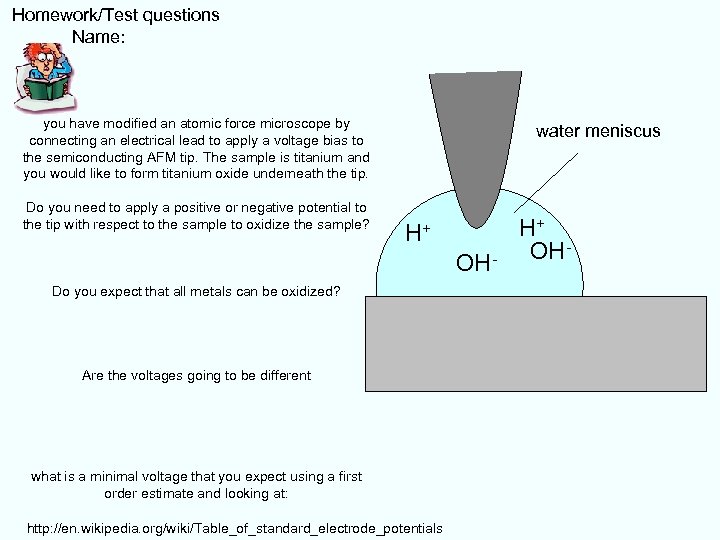 Homework/Test questions Name: you have modified an atomic force microscope by connecting an electrical lead to apply a voltage bias to the semiconducting AFM tip. The sample is titanium and you would like to form titanium oxide underneath the tip. Do you need to apply a positive or negative potential to the tip with respect to the sample to oxidize the sample? water meniscus H+ OH- Do you expect that all metals can be oxidized? Are the voltages going to be different what is a minimal voltage that you expect using a first order estimate and looking at: http: //en. wikipedia. org/wiki/Table_of_standard_electrode_potentials H+ OH-
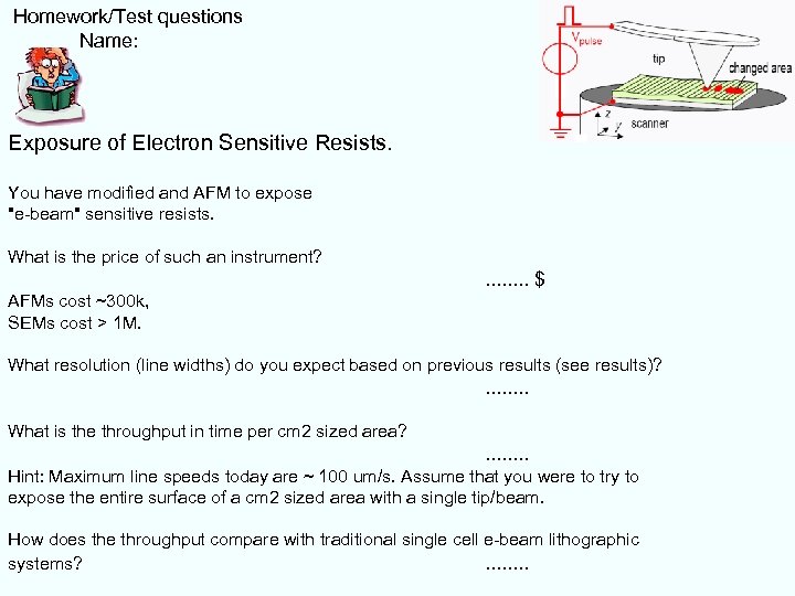 Homework/Test questions Name: Exposure of Electron Sensitive Resists. You have modified and AFM to expose "e-beam" sensitive resists. What is the price of such an instrument? . . . . $ AFMs cost ~300 k, SEMs cost > 1 M. What resolution (line widths) do you expect based on previous results (see results)? . . . . What is the throughput in time per cm 2 sized area? . . . . Hint: Maximum line speeds today are ~ 100 um/s. Assume that you were to try to expose the entire surface of a cm 2 sized area with a single tip/beam. How does the throughput compare with traditional single cell e-beam lithographic systems? . . . .
 Homework/Test questions Name: Explain how KFM can measure the local surface potential by filling in appropriate words: KFM detects localized. . . . forces between the tip and the sample to measure the surface potential of the sample. A . . is used to adjust the. . . tip . . . . until the. . . . force. . . At this point the DC tip. . . . is equal to the local surface. . .
 Homework/Test questions Name: How do you record charge patterns and surface potentials without touching the sample? KFM Kelvin Probe Force Microscopy --- A quick excurse to a special AFM to map electrical charges and potentials Name two physical effects that will cause a variation in the surface potential?
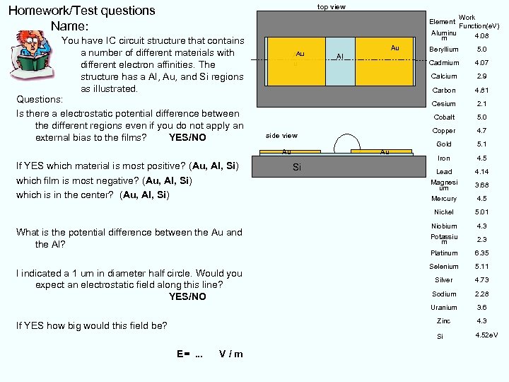 top view Homework/Test questions Name: Work Function(e. V) Aluminu 4. 08 m Element You have IC circuit structure that contains a number of different materials with different electron affinities. The structure has a Al, Au, and Si regions as illustrated. Questions: Is there a electrostatic potential difference between the different regions even if you do not apply an external bias to the films? YES/NO Au E=. . . V/m 4. 7 Gold 5. 1 Iron 4. 5 Lead 4. 14 Magnesi um 3. 68 Mercury 4. 5 5. 01 Niobium 4. 3 Potassiu m 2. 3 Platinum 6. 35 Selenium 5. 11 Silver 4. 73 Sodium 2. 28 3. 6 4. 3 Si If YES how big would this field be? Copper Zinc I indicated a 1 um in diameter half circle. Would you expect an electrostatic field along this line? YES/NO 5. 0 Uranium What is the potential difference between the Au and the Al? Si 2. 1 Nickel If YES which material is most positive? (Au, Al, Si) which film is most negative? (Au, Al, Si) which is in the center? (Au, Al, Si) 4. 81 Cobalt Au 2. 9 Cesium Au 4. 07 Carbon side view 5. 0 Cadmium Al Beryllium Calcium Au A u 4. 52 e. V
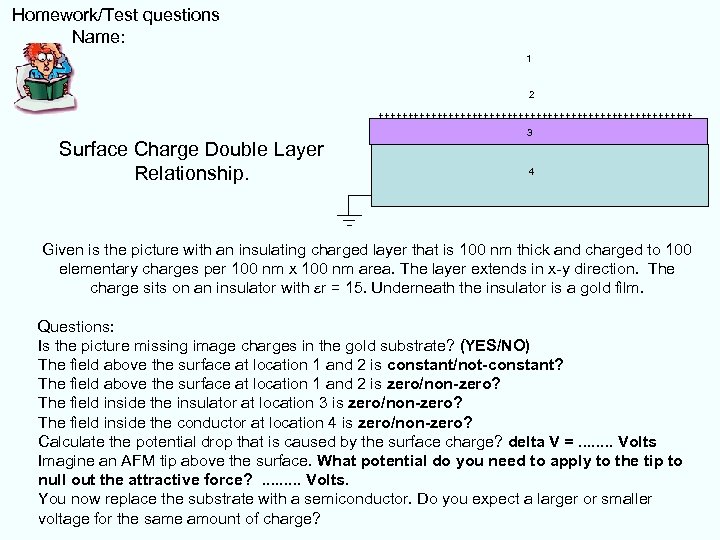 Homework/Test questions Name: 1 2 +++++++++++++++++++++++++++ Surface Charge Double Layer Relationship. 3 4 Given is the picture with an insulating charged layer that is 100 nm thick and charged to 100 elementary charges per 100 nm x 100 nm area. The layer extends in x-y direction. The charge sits on an insulator with er = 15. Underneath the insulator is a gold film. Questions: Is the picture missing image charges in the gold substrate? (YES/NO) The field above the surface at location 1 and 2 is constant/not-constant? The field above the surface at location 1 and 2 is zero/non-zero? The field inside the insulator at location 3 is zero/non-zero? The field inside the conductor at location 4 is zero/non-zero? Calculate the potential drop that is caused by the surface charge? delta V =. . . . Volts Imagine an AFM tip above the surface. What potential do you need to apply to the tip to null out the attractive force? . . Volts. You now replace the substrate with a semiconductor. Do you expect a larger or smaller voltage for the same amount of charge?
 Homework/Test questions Name: Soft Lithgraphy • Name two primary reasons why soft lithographic tools are being used? Hint: Compare with scanning probe lithography, compare with projection lithography. . • - How do you fabricate a mold? < Three sentences - How is a PDMS stamp made? < Three sentences • - Describe the key steps on how to print a self-assembled monolayer (SAM) using a PDMS stamp? • - How do you check if you succeeded in printing a SAM with -COOH or -CH 3 end groups ? • -You have made an e-beam pattern in PMMA and would like to make a replica without going back to the e-beam writer. Describe a two step process that gets you a replica in PMMA < Three sentences
 Homework/Test questions Name: • Why is the resolution limited in Soft. Lithography? • Describe the concept of Phaseshift Photolithography
 Homework/Test questions Name: Pervious Slides include the Material up to First Midterm
 Homework/Test questions Name: • L 11
 Homework/Test questions Name: Write down 5 different physical properties that change and a reason why other than size.
 Homework/Test questions Name: Write down the primary reason why the crystal lattice constant becomes smaller.
 Homework/Test questions Name: Added DEC 2010 Nanomaterials demonstrate decreased conductivity with decreasing size due to _____ as well as increased conductivity with decreasing size due to ______.
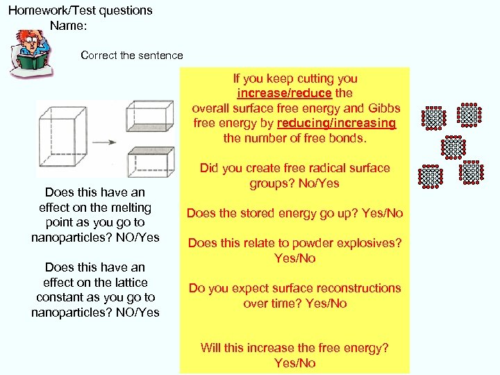 Homework/Test questions Name: Correct the sentence If you keep cutting you increase/reduce the overall surface free energy and Gibbs free energy by reducing/increasing the number of free bonds. Did you create free radical surface groups? No/Yes Does this have an effect on the melting point as you go to nanoparticles? NO/Yes Does the stored energy go up? Yes/No Does this have an effect on the lattice constant as you go to nanoparticles? NO/Yes Do you expect surface reconstructions over time? Yes/No Does this relate to powder explosives? Yes/No Will this increase the free energy? Yes/No
 Homework/Test questions Name: Self-Assembled Monolayers can Change the Surface Free Energy. A nanocrystal has been passivated and the surface free energy has been reduced. Do you expect it to be under reduced "compression"? What do you expect in terms of lattice constant?
 Homework/Test questions Name: Name the primary two reasons for an increased hardness in the case of nanowiskers?
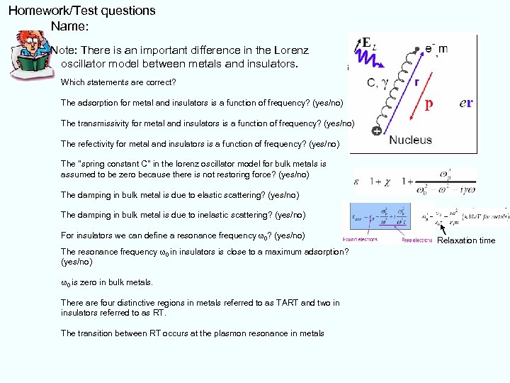 Homework/Test questions Name: Note: There is an important difference in the Lorenz oscillator model between metals and insulators. Which statements are correct? The adsorption for metal and insulators is a function of frequency? (yes/no) The transmissivity for metal and insulators is a function of frequency? (yes/no) The refectivity for metal and insulators is a function of frequency? (yes/no) The "spring constant C" in the lorenz oscillator model for bulk metals is assumed to be zero because there is not restoring force? (yes/no) The damping in bulk metal is due to elastic scattering? (yes/no) The damping in bulk metal is due to inelastic scattering? (yes/no) For insulators we can define a resonance frequency w 0? (yes/no) The resonance frequency w 0 in insulators is close to a maximum adsorption? (yes/no) w 0 is zero in bulk metals. There are four distinctive regions in metals referred to as TART and two in insulators referred to as RT. The transition between RT occurs at the plasmon resonance in metals Relaxation time
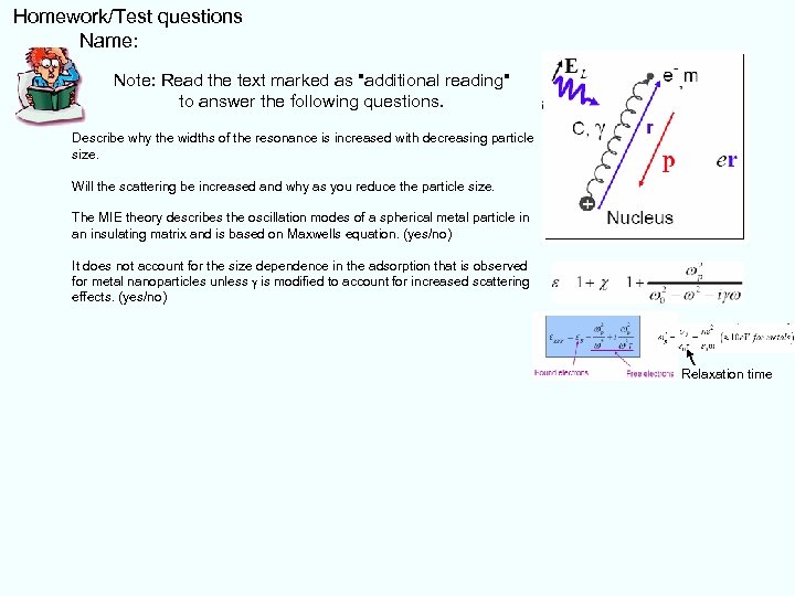 Homework/Test questions Name: Note: Read the text marked as "additional reading" to answer the following questions. Describe why the widths of the resonance is increased with decreasing particle size. Will the scattering be increased and why as you reduce the particle size. The MIE theory describes the oscillation modes of a spherical metal particle in an insulating matrix and is based on Maxwells equation. (yes/no) It does not account for the size dependence in the adsorption that is observed for metal nanoparticles unless g is modified to account for increased scattering effects. (yes/no) Relaxation time
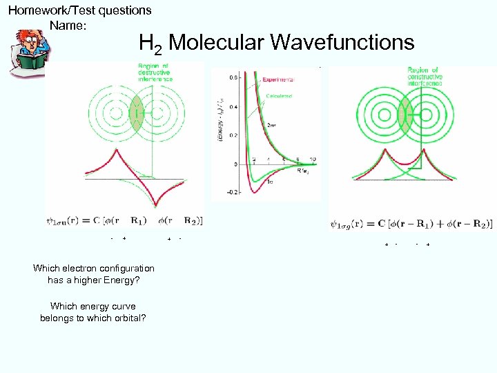 Homework/Test questions Name: H 2 Molecular Wavefunctions - + Which electron configuration has a higher Energy? Which energy curve belongs to which orbital? + - - +
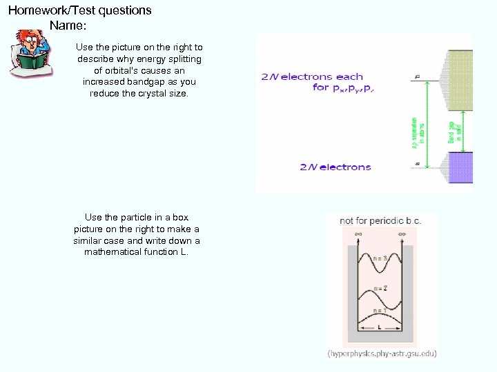 Homework/Test questions Name: Use the picture on the right to describe why energy splitting of orbital's causes an increased bandgap as you reduce the crystal size. Use the particle in a box picture on the right to make a similar case and write down a mathematical function L.
 Homework/Test questions Name: • L 15
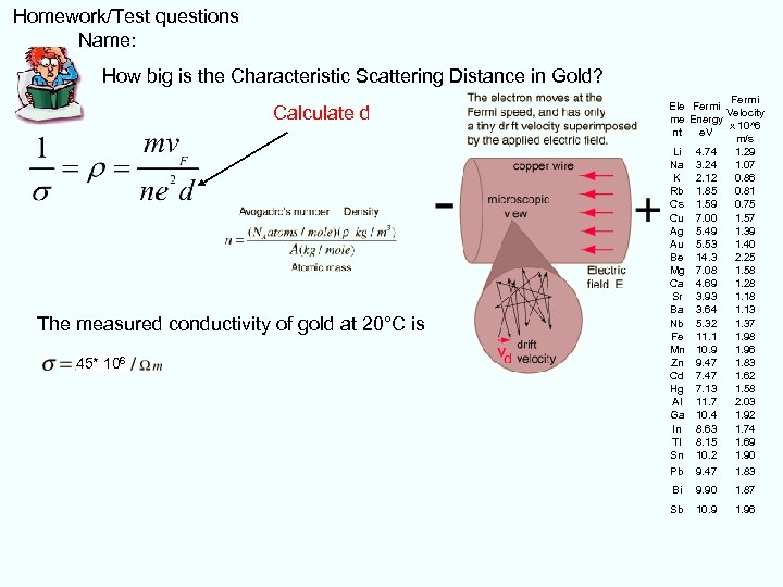 Homework/Test questions Name: How big is the Characteristic Scattering Distance in Gold? Calculate d The measured conductivity of gold at 20°C is 45* 106 Fermi Ele Fermi Velocity me Energy x 10^6 nt e. V m/s Li 4. 74 1. 29 Na 3. 24 1. 07 K 2. 12 0. 86 Rb 1. 85 0. 81 Cs 1. 59 0. 75 Cu 7. 00 1. 57 Ag 5. 49 1. 39 Au 5. 53 1. 40 Be 14. 3 2. 25 Mg 7. 08 1. 58 Ca 4. 69 1. 28 Sr 3. 93 1. 18 Ba 3. 64 1. 13 Nb 5. 32 1. 37 Fe 11. 1 1. 98 Mn 10. 9 1. 96 Zn 9. 47 1. 83 Cd 7. 47 1. 62 Hg 7. 13 1. 58 Al 11. 7 2. 03 Ga 10. 4 1. 92 In 8. 63 1. 74 Tl 8. 15 1. 69 Sn 10. 2 1. 90 Pb 9. 47 1. 83 Bi 9. 90 1. 87 Sb 10. 9 1. 96
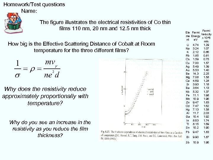 Homework/Test questions Name: The figure illustrates the electrical resistivities of Co thin films 110 nm, 20 nm and 12. 5 nm thick How big is the Effective Scattering Distance of Cobalt at Room temperature for the three different films? Why does the resistivity reduce approximately proportionally with temperature? Why do you see an increase in the resistivity as you reduce the film thickness? Fermi Ele Fermi Velocity me Energy x 10^6 nt e. V m/s Li 4. 74 1. 29 Na 3. 24 1. 07 K 2. 12 0. 86 Rb 1. 85 0. 81 Cs 1. 59 0. 75 Cu 7. 00 1. 57 Ag 5. 49 1. 39 Au 5. 53 1. 40 Be 14. 3 2. 25 Mg 7. 08 1. 58 Ca 4. 69 1. 28 Sr 3. 93 1. 18 Ba 3. 64 1. 13 Nb 5. 32 1. 37 Fe 11. 1 1. 98 Mn 10. 9 1. 96 Zn 9. 47 1. 83 Cd 7. 47 1. 62 Hg 7. 13 1. 58 Al 11. 7 2. 03 Ga 10. 4 1. 92 In 8. 63 1. 74 Tl 8. 15 1. 69 Sn 10. 2 1. 90 Pb 9. 47 1. 83 Bi 9. 90 1. 87 Sb 10. 9 1. 96
 Homework/Test questions Name: • For ballistic transport to occur the physical device dimensions have to be smaller/larger (cancel) than the electron mean free path. • Write down an simple equation that relates the potential drop (E = V) with the gained velocity considering ballistic transport without any scattering. added:
 Homework/Test questions Name: Describe a mechanism by which semiconducting nanowires can become insulating as you shrink down the size.
 Homework/Test questions Name: • L 17
 Homework/Test questions Name: Why do nanoparticles or wires show distinct crystal facets? Do these facets represent an energy minimum? Yes/No Do you expect them to have a larger number of dangling bonds than other configurations that are less likely? Yes/No Will all nanomaterials form facets? Yes/No, Explain.
 Homework/Test questions Name: Describe what happens when you increase your solute concentration over the equilibrium concentration of your solute? Describe the concept of Oswald Ripening -- what happens to the embryos and what happens to the nuclei and what happens to the solute concentration?
 Homework/Test questions Name: Describe how you can prevent agglomeration through charge stabilization: (a few sentences) What are the parameter that you can adjust? Is it good to be working at the P. Z. C point? Yes/No Would you like to have a large Surface Potential? Yes/No Is a larger double layer thickness advantageous? Yes/No Would you like to have a large or small counter ion concentration? Large/small
 Homework/Test questions Name: added: Describe how gold nanoparticles were used as a Na. Cl sensor. What happens to the nanoparticles as you increase the Na. Cl concentration and why? What is the change that you observe with your eye and why?
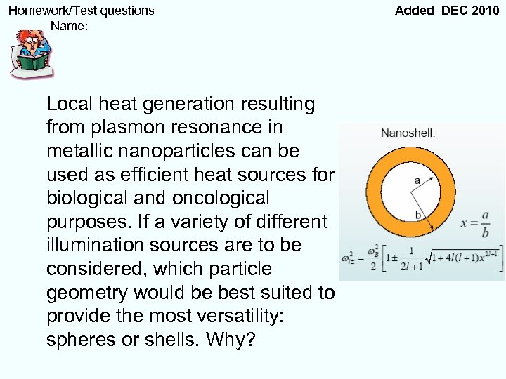 Homework/Test questions Name: Local heat generation resulting from plasmon resonance in metallic nanoparticles can be used as efficient heat sources for biological and oncological purposes. If a variety of different illumination sources are to be considered, which particle geometry would be best suited to provide the most versatility: spheres or shells. Why? Added DEC 2010
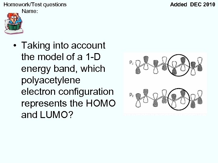 Homework/Test questions Name: • Taking into account the model of a 1 -D energy band, which polyacetylene electron configuration represents the HOMO and LUMO? Added DEC 2010
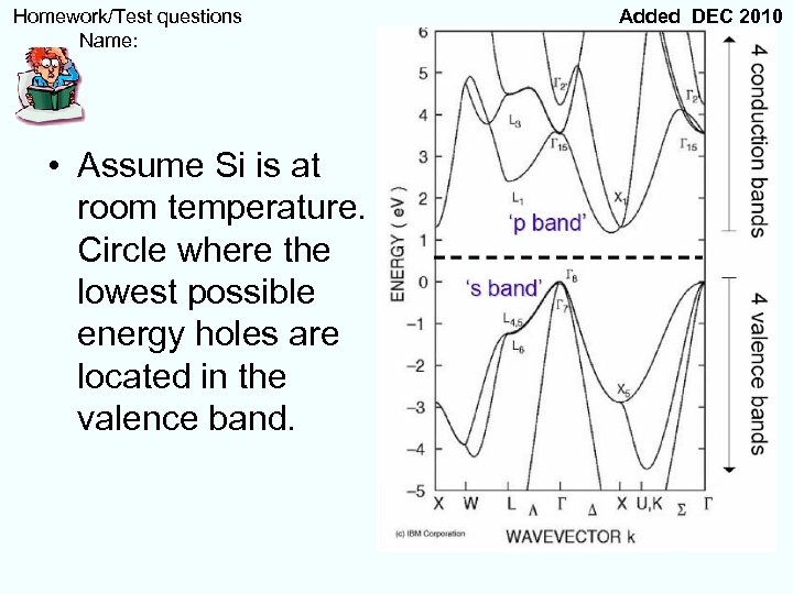 Homework/Test questions Name: • Assume Si is at room temperature. Circle where the lowest possible energy holes are located in the valence band. Added DEC 2010
 Homework/Test questions Name: Added DEC 2010 • At what size will quantum size effects occur for a nanocrystal? • At this size, a particle is transitioning between which two electron state regimes?
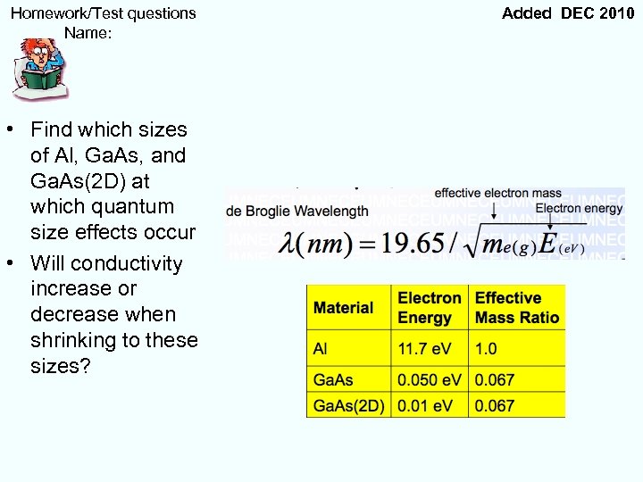 Homework/Test questions Name: • Find which sizes of Al, Ga. As, and Ga. As(2 D) at which quantum size effects occur • Will conductivity increase or decrease when shrinking to these sizes? Added DEC 2010
 Homework/Test questions Name: Added DEC 2010 • Describe the mechanisms of thermal and defect resistivity and how they related to the total resistivity of a material
 Homework/Test questions Name: Added DEC 2010 In ballistic transport: • Electrons have so much energy, they must dissipate some of it as heat (True/False) • There cannot be impurities present (True/False) • Elastic and not inelastic scattering is observed (True/False) • Device dimensions are less that the electron mean free path (True/False) • Very high current densities can be observed (True/False)
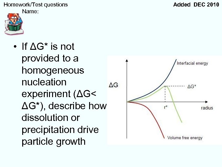 Homework/Test questions Name: • If ΔG* is not provided to a homogeneous nucleation experiment (ΔG< ΔG*), describe how dissolution or precipitation drive particle growth Added DEC 2010
 Homework/Test questions Name: Added DEC 2010 • Describe a method for fabricating flexible electrodes with low bend radii on PDMS
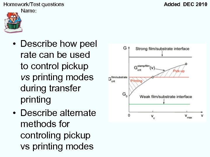 Homework/Test questions Name: • Describe how peel rate can be used to control pickup vs printing modes during transfer printing • Describe alternate methods for controling pickup vs printing modes Added DEC 2010
 Homework/Test questions Name: • L 21
 Homework/Test questions Name: • Nanoxerographic printing from a powder has a limited resolution. Name the primary reason why the resolution is limited. Hint the reason are has to do with the particles. • Consider Iron Oxide as a primary particle. Is the surface hydrophobic? • TEM studies have shown that the primary particle size is 10 nm. What will happen to particles in a powder form and why?
 Homework/Test questions Name: • Nanoxerographic printing in a liquid has a limited resolution. Name the primary reason why the resolution is limited. Hint the reason has to do with the particles. • The assembly works only in non-polar solvents. Describe why? • Based on previous lectures what happens in water (remember water contains H+ and OH-) to the electric field. What was a typical screening length? 10 nm or 10 um choose one. • You have learned methods to prevent particle aggregation in solution will they work in this case? • How about using a non-polar polymer brush surrounding the particles?
 Homework/Test questions Name: • L 22
 Homework/Test questions Name: Review the coursework material and identify forces that can be neglected in the design of self-assembly processes. Consider all length scales (1 nm-1 mm). Cancel out the identified forces in the list: weak and strong interactions between neutrons and protons gravitational forces ionic&covalent&hydrogen bonds Van-de-Waals forces magnetic forces ionic&covalent&hydrogen bonds, coulomb forces, Hydrophobic/hydrophilic interaction, capillary forces, surface tension drag force Brownian motion
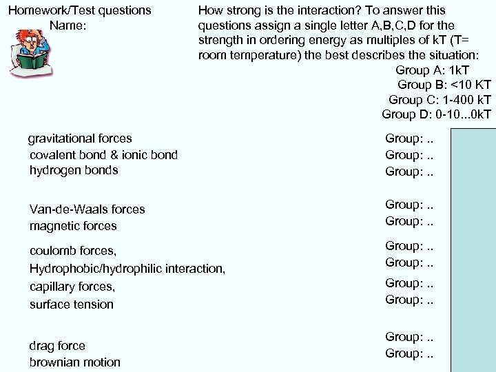 Homework/Test questions Name: How strong is the interaction? To answer this questions assign a single letter A, B, C, D for the strength in ordering energy as multiples of k. T (T= room temperature) the best describes the situation: Group A: 1 k. T Group B: <10 KT Group C: 1 -400 k. T Group D: 0 -10. . . 0 k. T gravitational forces covalent bond & ionic bond hydrogen bonds Van-de-Waals forces magnetic forces coulomb forces, Hydrophobic/hydrophilic interaction, capillary forces, surface tension drag force brownian motion Group: . . 1 point 1 point Group: . . 1 point
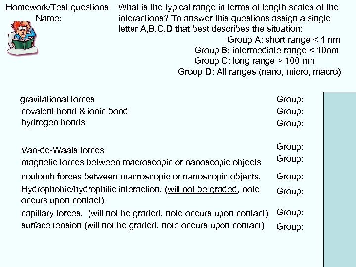 Homework/Test questions Name: What is the typical range in terms of length scales of the interactions? To answer this questions assign a single letter A, B, C, D that best describes the situation: Group A: short range < 1 nm Group B: intermediate range < 10 nm Group C: long range > 100 nm Group D: All ranges (nano, micro, macro) gravitational forces covalent bond & ionic bond hydrogen bonds Van-de-Waals forces magnetic forces between macroscopic or nanoscopic objects coulomb forces between macroscopic or nanoscopic objects, Hydrophobic/hydrophilic interaction, (will not be graded, note occurs upon contact) capillary forces, (will not be graded, note occurs upon contact) surface tension (will not be graded, note occurs upon contact) Group: Group: 1 point Group: 1 point
 Homework/Test questions Name: Describe three different concepts to integrate Nanoparticles in addressable regions on a surface?
 Homework/Test questions Name: Describe a technology that allows you to integrate a Nanowires at precise locations on a surface. The technology should allow to both control the location and diameter of the nanowire.
 Homework/Test questions Name: Describe a technology that allows you to control the in plane orientation of nanowires. How do you fabricate crossed wire arrays?
 Homework/Test questions Name: Considering the Scaling Laws. What do you think is the expected range for surface tension directed selfassembly processes? Hint: at what approximate scales will gravity matter? at what approximate scales will Brownian motion matter? Can you eliminate gravity? Can you eliminate electrostatic forces in your experiment? If yes how? Can you eliminate drag forces in your experiment? If yes how?
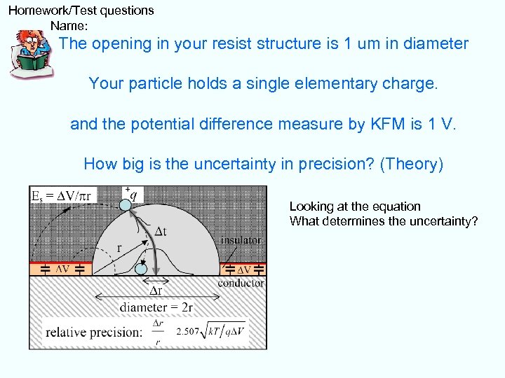 Homework/Test questions Name: The opening in your resist structure is 1 um in diameter Your particle holds a single elementary charge. and the potential difference measure by KFM is 1 V. How big is the uncertainty in precision? (Theory) Looking at the equation What determines the uncertainty?
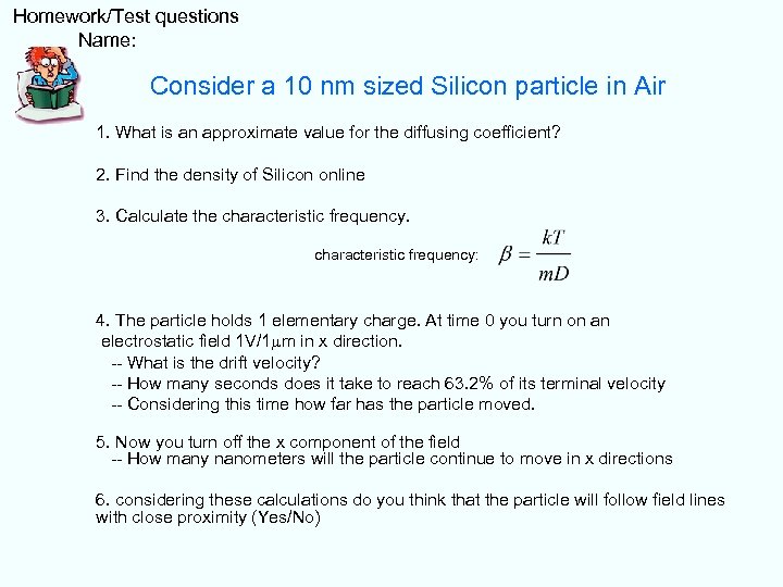 Homework/Test questions Name: Consider a 10 nm sized Silicon particle in Air 1. What is an approximate value for the diffusing coefficient? 2. Find the density of Silicon online 3. Calculate the characteristic frequency: 4. The particle holds 1 elementary charge. At time 0 you turn on an electrostatic field 1 V/1 mm in x direction. -- What is the drift velocity? -- How many seconds does it take to reach 63. 2% of its terminal velocity -- Considering this time how far has the particle moved. 5. Now you turn off the x component of the field -- How many nanometers will the particle continue to move in x directions 6. considering these calculations do you think that the particle will follow field lines with close proximity (Yes/No)
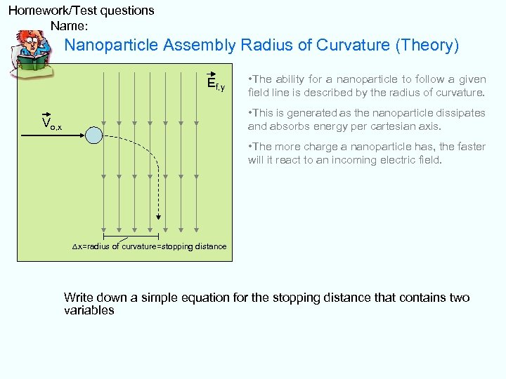 Homework/Test questions Name: Nanoparticle Assembly Radius of Curvature (Theory) Ef, y • The ability for a nanoparticle to follow a given field line is described by the radius of curvature. • This is generated as the nanoparticle dissipates and absorbs energy per cartesian axis. Vo, x • The more charge a nanoparticle has, the faster will it react to an incoming electric field. ∆x=radius of curvature=stopping distance Write down a simple equation for the stopping distance that contains two variables


