a4fd2d87eaf072c342666090468f8479.ppt
- Количество слайдов: 99
 High-Speed Digital Logic Chris Allen (callen@eecs. ku. edu) Course website URL people. eecs. ku. edu/~callen/713/EECS 713. htm 1
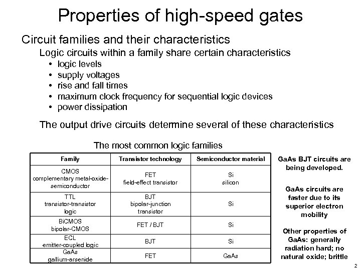 Properties of high-speed gates Circuit families and their characteristics Logic circuits within a family share certain characteristics • • • logic levels supply voltages rise and fall times maximum clock frequency for sequential logic devices power dissipation The output drive circuits determine several of these characteristics The most common logic families Family Transistor technology Semiconductor material CMOS complementary metal-oxidesemiconductor FET field-effect transistor Si silicon TTL transistor-transistor logic BJT bipolar-junction transistor Si FET / BJT Si FET Ga. As Bi. CMOS bipolar-CMOS ECL emitter-coupled logic Ga. As gallium-arsenide Ga. As BJT circuits are being developed. Ga. As circuits are faster due to its superior electron mobility Other properties of Ga. As: generally radiation hard; no natural oxide; brittle 2
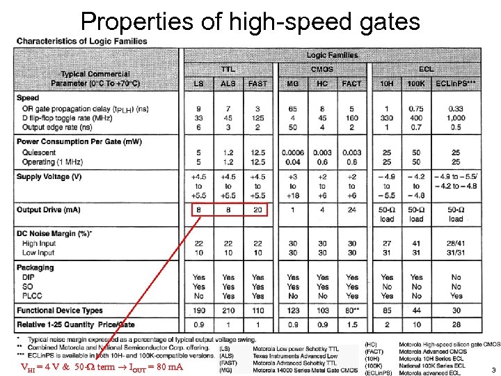 Properties of high-speed gates VHI = 4 V & 50 - term IOUT = 80 m. A 3
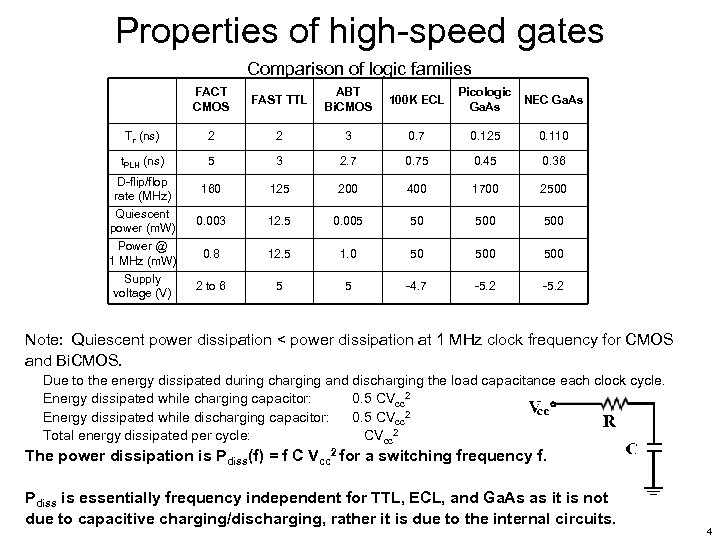 Properties of high-speed gates Comparison of logic families FACT CMOS FAST TTL ABT Bi. CMOS 100 K ECL Picologic Ga. As NEC Ga. As Tr (ns) 2 2 3 0. 7 0. 125 0. 110 t. PLH (ns) 5 3 2. 7 0. 75 0. 45 0. 36 160 125 200 400 1700 2500 0. 003 12. 5 0. 005 50 500 0. 8 12. 5 1. 0 50 500 2 to 6 5 5 -4. 7 -5. 2 D-flip/flop rate (MHz) Quiescent power (m. W) Power @ 1 MHz (m. W) Supply voltage (V) Note: Quiescent power dissipation < power dissipation at 1 MHz clock frequency for CMOS and Bi. CMOS. Due to the energy dissipated during charging and discharging the load capacitance each clock cycle. Energy dissipated while charging capacitor: 0. 5 CVcc 2 Energy dissipated while discharging capacitor: 0. 5 CVcc 2 Total energy dissipated per cycle: CVcc 2 The power dissipation is Pdiss(f) = f C Vcc 2 for a switching frequency f. Pdiss is essentially frequency independent for TTL, ECL, and Ga. As as it is not due to capacitive charging/discharging, rather it is due to the internal circuits. 4
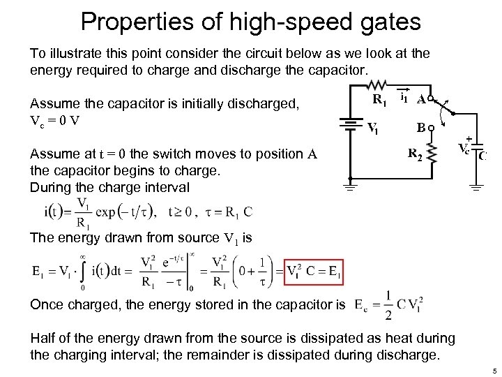 Properties of high-speed gates To illustrate this point consider the circuit below as we look at the energy required to charge and discharge the capacitor. Assume the capacitor is initially discharged, Vc = 0 V Assume at t = 0 the switch moves to position A the capacitor begins to charge. During the charge interval The energy drawn from source V 1 is Once charged, the energy stored in the capacitor is Half of the energy drawn from the source is dissipated as heat during the charging interval; the remainder is dissipated during discharge. 5
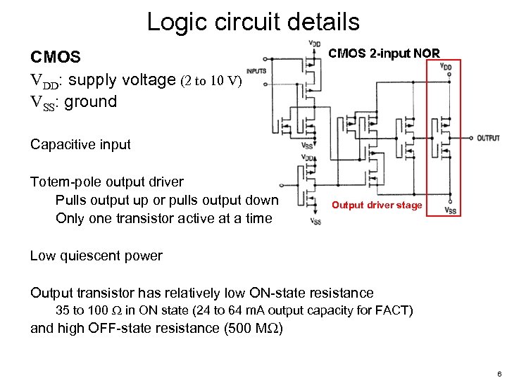 Logic circuit details CMOS VDD: supply voltage (2 to 10 V) VSS: ground Capacitive input Totem-pole output driver Pulls output up or pulls output down Only one transistor active at a time Output driver stage Low quiescent power Output transistor has relatively low ON-state resistance 35 to 100 in ON state (24 to 64 m. A output capacity for FACT) and high OFF-state resistance (500 M ) 6
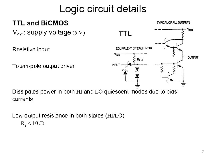 Logic circuit details TTL and Bi. CMOS VCC: supply voltage (5 V) Resistive input Totem-pole output driver Dissipates power in both HI and LO quiescent modes due to bias currents Low output resistance in both states (HI/LO) Rs < 10 7
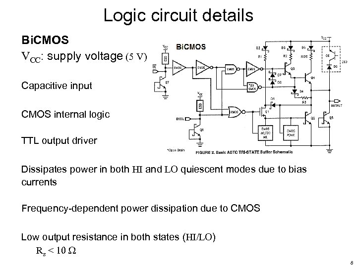 Logic circuit details Bi. CMOS VCC: supply voltage (5 V) Capacitive input CMOS internal logic TTL output driver Dissipates power in both HI and LO quiescent modes due to bias currents Frequency-dependent power dissipation due to CMOS Low output resistance in both states (HI/LO) Rs < 10 8
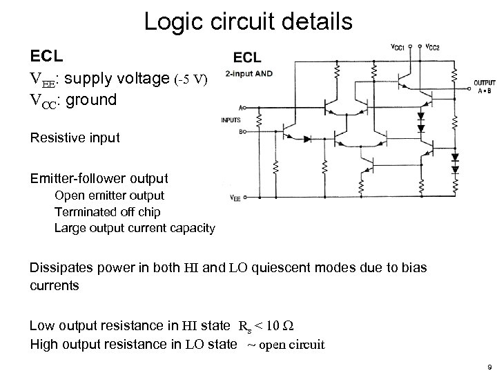 Logic circuit details ECL VEE: supply voltage (-5 V) VCC: ground Resistive input Emitter-follower output Open emitter output Terminated off chip Large output current capacity Dissipates power in both HI and LO quiescent modes due to bias currents Low output resistance in HI state Rs < 10 High output resistance in LO state ~ open circuit 9
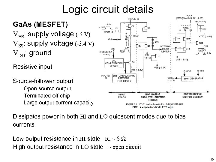 Logic circuit details Ga. As (MESFET) VEE: supply voltage (-5 V) VSS: supply voltage (-3. 4 V) VDD: ground Resistive input Source-follower output Open source output Terminated off chip Large output current capacity Dissipates power in both HI and LO quiescent modes due to bias currents Low output resistance in HI state Rs ~ 8 High output resistance in LO state ~ open circuit 10
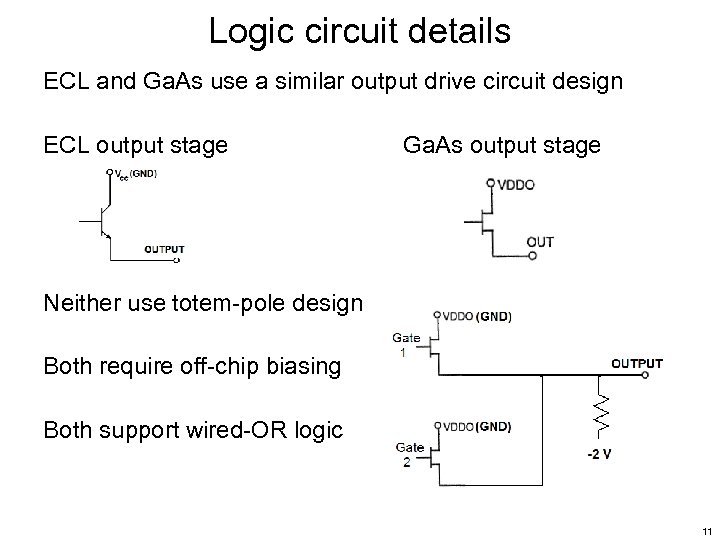 Logic circuit details ECL and Ga. As use a similar output drive circuit design ECL output stage Ga. As output stage Neither use totem-pole design Both require off-chip biasing Both support wired-OR logic 11
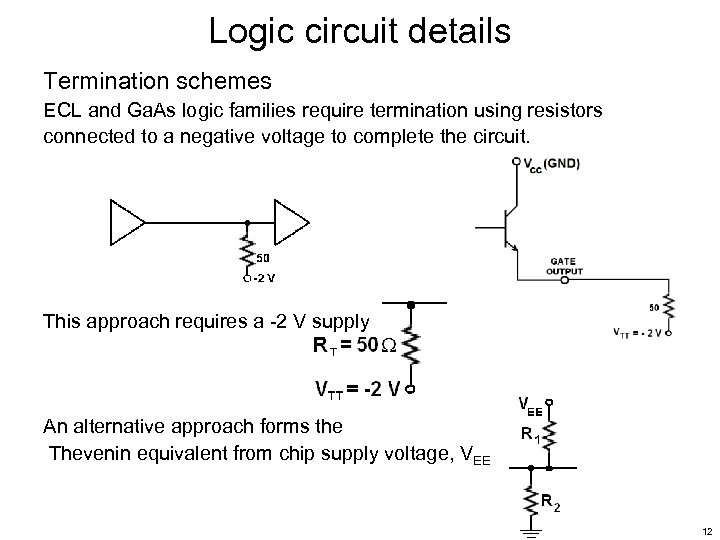 Logic circuit details Termination schemes ECL and Ga. As logic families require termination using resistors connected to a negative voltage to complete the circuit. This approach requires a -2 V supply An alternative approach forms the Thevenin equivalent from chip supply voltage, VEE 12
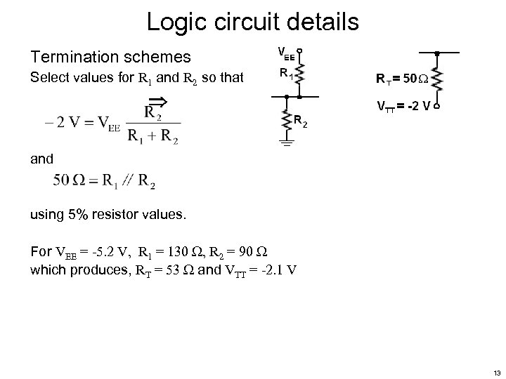 Logic circuit details Termination schemes Select values for R 1 and R 2 so that and using 5% resistor values. For VEE = -5. 2 V, R 1 = 130 , R 2 = 90 which produces, RT = 53 and VTT = -2. 1 V 13
 Logic circuit details Faster technologies cost more In terms of $ In terms of Pdiss In terms of design complexity Don’t use technology with more capability than needed Recall that Tr Fknee • Fknee = 0. 5 / Tr Bandwidth over which signal fidelity must be preserved More reflections, ringing • • More crosstalk higher d. I/dt increases inductive crosstalk higher d. V/dt increases capacitive crosstalk Therefore, use technology with the slowest acceptable Tr 14
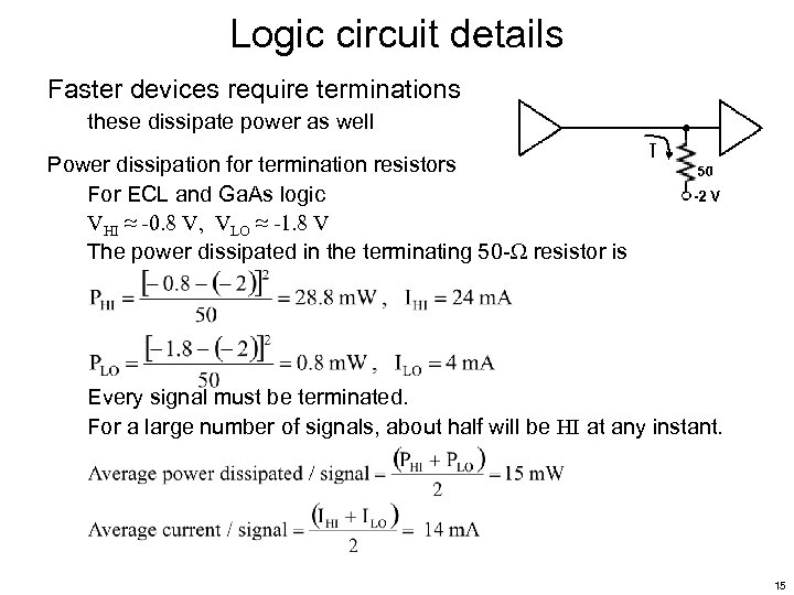 Logic circuit details Faster devices require terminations these dissipate power as well Power dissipation for termination resistors For ECL and Ga. As logic VHI ≈ -0. 8 V, VLO ≈ -1. 8 V The power dissipated in the terminating 50 - resistor is Every signal must be terminated. For a large number of signals, about half will be HI at any instant. 15
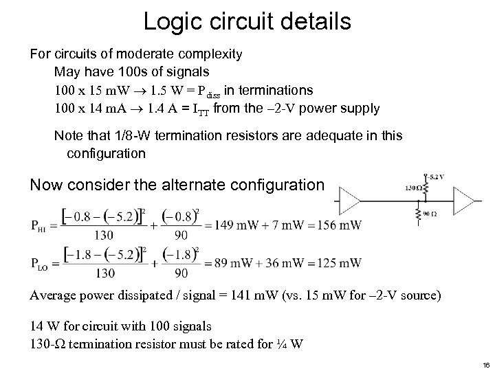 Logic circuit details For circuits of moderate complexity May have 100 s of signals 100 x 15 m. W 1. 5 W = Pdiss in terminations 100 x 14 m. A 1. 4 A = ITT from the – 2 -V power supply Note that 1/8 -W termination resistors are adequate in this configuration Now consider the alternate configuration Average power dissipated / signal = 141 m. W (vs. 15 m. W for – 2 -V source) 14 W for circuit with 100 signals 130 - termination resistor must be rated for ¼ W 16
 Noise margins Digital-signal transmission has superior signal preservation compared to analog transmission Digital signaling has “built-in” tolerance to noise, crosstalk, voltage variations, ringing or reflections, temperature variations, EMI, and other sources of signal distortion … as long as bit errors can be avoided. To avoid bit errors, a transmitted HI must be reliably received as a HI, and similarly a transmitted LO, received as a LO Digital communication can tolerate limited channel error sources due to noise margins The difference between the transmitted signal level and the decision threshold level is the noise margin. As long as a logical HI signal is above a given threshold level, it will be read as a HI, likewise for LO signals. 17
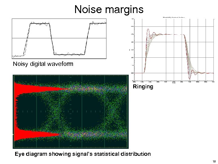 Noise margins Noisy digital waveform Ringing Eye diagram showing signal’s statistical distribution 18
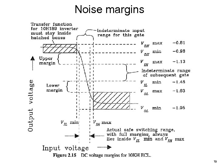 Noise margins 19
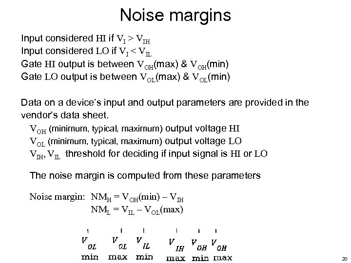 Noise margins Input considered HI if VI > VIH Input considered LO if VI < VIL Gate HI output is between VOH(max) & VOH(min) Gate LO output is between VOL(max) & VOL(min) Data on a device’s input and output parameters are provided in the vendor’s data sheet. VOH (minimum, typical, maximum) output voltage HI VOL (minimum, typical, maximum) output voltage LO VIH, VIL threshold for deciding if input signal is HI or LO The noise margin is computed from these parameters Noise margin: NMH = VOH(min) – VIH NML = VIL – VOL(max) 20
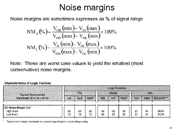 Noise margins are sometimes expresses as % of signal range Note: These are worst case values to yield the smallest (most conservative) noise margins. 21
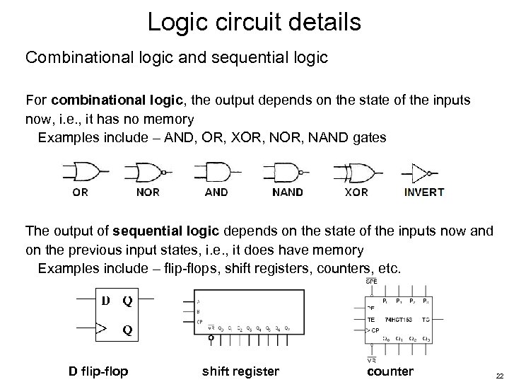 Logic circuit details Combinational logic and sequential logic For combinational logic, the output depends on the state of the inputs now, i. e. , it has no memory Examples include – AND, OR, XOR, NAND gates The output of sequential logic depends on the state of the inputs now and on the previous input states, i. e. , it does have memory Examples include – flip-flops, shift registers, counters, etc. D flip-flop shift register counter 22
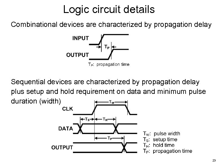 Logic circuit details Combinational devices are characterized by propagation delay Sequential devices are characterized by propagation delay plus setup and hold requirement on data and minimum pulse duration (width) 23
 Timing analysis High-speed designs require timing analysis that includes • • • Propagation delays through devices Propagation delays through interconnects (traces) Data setup times Data hold times Pulse durations Reliable designs anticipate worst case conditions To find the elapsed time as a signal propagates through a signal path, individual propagation delays are added. In clocked (sequential) systems, the signal must arrive and be stable for the required time before the clock edge arrives. In some designs, multiple signal paths must be analyzed to determine the circuit’s highest operating frequency. 24
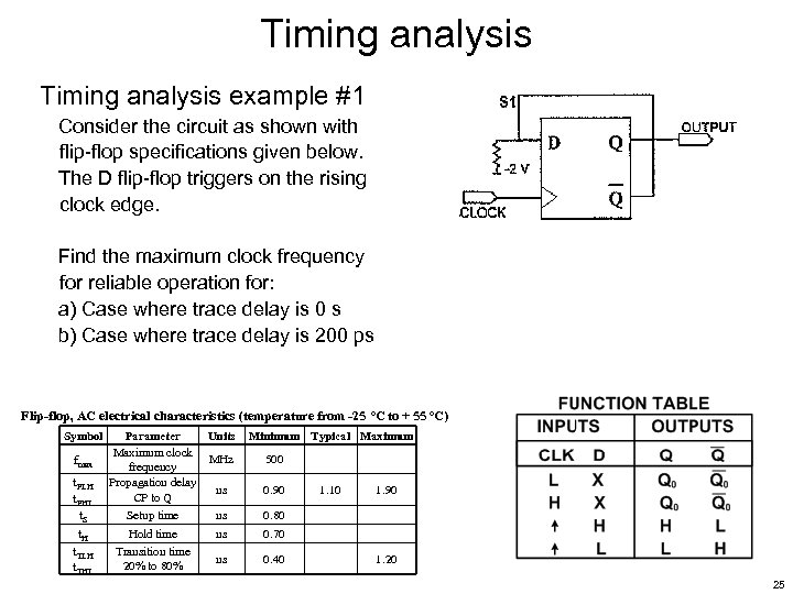 Timing analysis example #1 Consider the circuit as shown with flip-flop specifications given below. The D flip-flop triggers on the rising clock edge. Find the maximum clock frequency for reliable operation for: a) Case where trace delay is 0 s b) Case where trace delay is 200 ps Flip-flop, AC electrical characteristics (temperature from -25 ºC to + 55 ºC) Symbol fmax t. PLH t. PHL t. S t. H t. TLH t. THL Parameter Units Maximum clock MHz frequency Propagation delay ns CP to Q Setup time ns Hold time Transition time 20% to 80% Minimum Typical Maximum 500 0. 90 1. 10 1. 90 0. 80 ns 0. 70 ns 0. 40 1. 20 25
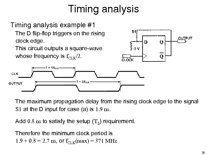 Timing analysis example #1 The D flip-flop triggers on the rising clock edge. This circuit outputs a square-wave whose frequency is f. CLK/2. The maximum propagation delay from the rising clock edge to the signal S 1 at the D input for case (a) is 1. 9 ns. Add 0. 8 ns to satisfy the setup (TS) requirement. Therefore the minimum clock period is 1. 9 + 0. 8 = 2. 7 ns, or f. CLK(max) = 371 MHz 26
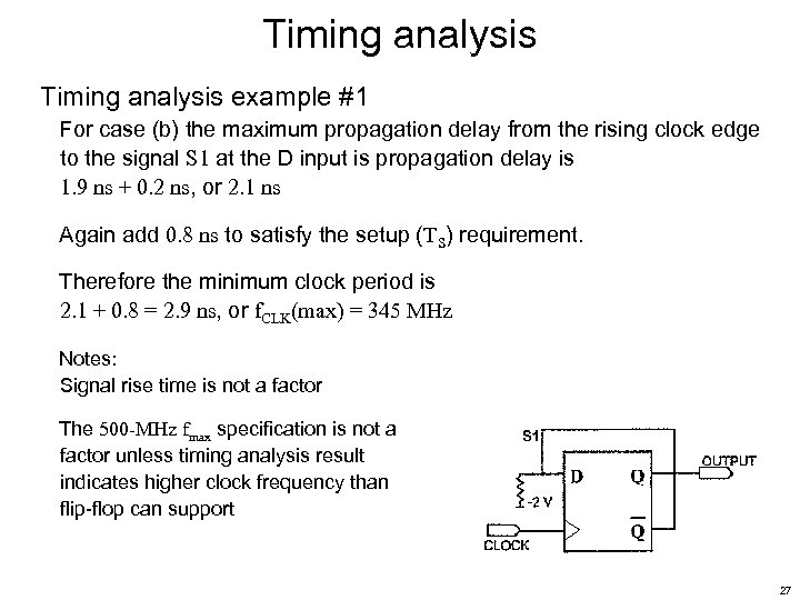 Timing analysis example #1 For case (b) the maximum propagation delay from the rising clock edge to the signal S 1 at the D input is propagation delay is 1. 9 ns + 0. 2 ns, or 2. 1 ns Again add 0. 8 ns to satisfy the setup (TS) requirement. Therefore the minimum clock period is 2. 1 + 0. 8 = 2. 9 ns, or f. CLK(max) = 345 MHz Notes: Signal rise time is not a factor The 500 -MHz fmax specification is not a factor unless timing analysis result indicates higher clock frequency than flip-flop can support 27
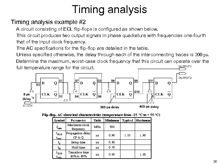 Timing analysis example #2 A circuit consisting of ECL flip-flops is configured as shown below. This circuit produces two output signals in phase quadrature with frequencies one-fourth that of the input clock frequency. The AC specifications for the flip-flop are detailed in the table. Unless specified otherwise, the delay through each of the interconnecting traces is 200 ps. Determine the maximum, worst-case clock frequency that this circuit can operate over the full temperature range for the circuit. Flip-flop, AC electrical characteristics (temperature from -25 ºC to + 55 ºC) Symbol fmax t. PLH t. PHL t. S t. H t. TLH t. THL Parameter Units Maximum clock MHz frequency Propagation delay ns CP to Q Setup time ns Hold time Transition time 20% to 80% Minimum Typical Maximum 500 0. 90 1. 10 1. 90 0. 80 ns 0. 70 ns 0. 40 1. 20 28
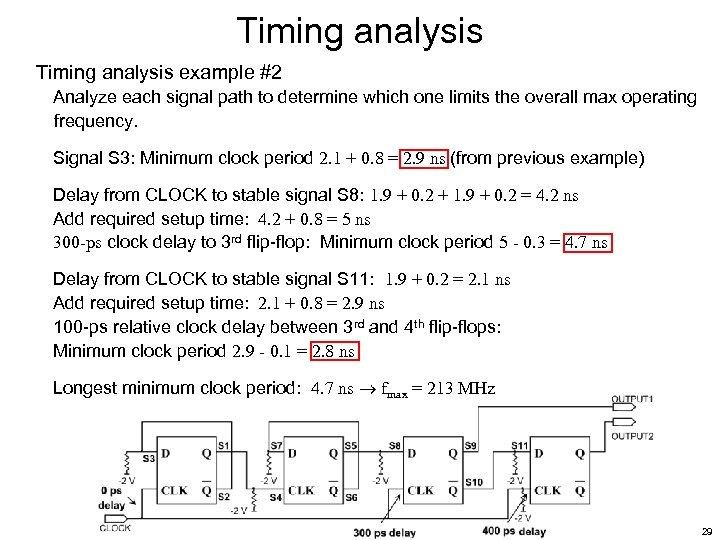 Timing analysis example #2 Analyze each signal path to determine which one limits the overall max operating frequency. Signal S 3: Minimum clock period 2. 1 + 0. 8 = 2. 9 ns (from previous example) Delay from CLOCK to stable signal S 8: 1. 9 + 0. 2 + 1. 9 + 0. 2 = 4. 2 ns Add required setup time: 4. 2 + 0. 8 = 5 ns 300 -ps clock delay to 3 rd flip-flop: Minimum clock period 5 - 0. 3 = 4. 7 ns Delay from CLOCK to stable signal S 11: 1. 9 + 0. 2 = 2. 1 ns Add required setup time: 2. 1 + 0. 8 = 2. 9 ns 100 -ps relative clock delay between 3 rd and 4 th flip-flops: Minimum clock period 2. 9 - 0. 1 = 2. 8 ns Longest minimum clock period: 4. 7 ns fmax = 213 MHz 29
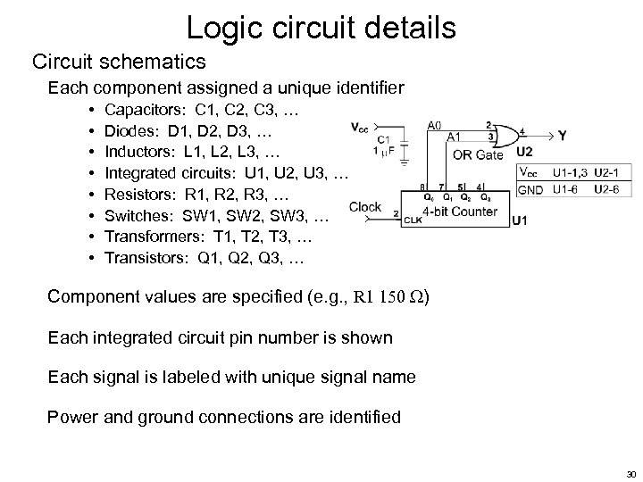 Logic circuit details Circuit schematics Each component assigned a unique identifier • • Capacitors: C 1, C 2, C 3, … Diodes: D 1, D 2, D 3, … Inductors: L 1, L 2, L 3, … Integrated circuits: U 1, U 2, U 3, … Resistors: R 1, R 2, R 3, … Switches: SW 1, SW 2, SW 3, … Transformers: T 1, T 2, T 3, … Transistors: Q 1, Q 2, Q 3, … Component values are specified (e. g. , R 1 150 ) Each integrated circuit pin number is shown Each signal is labeled with unique signal name Power and ground connections are identified 30
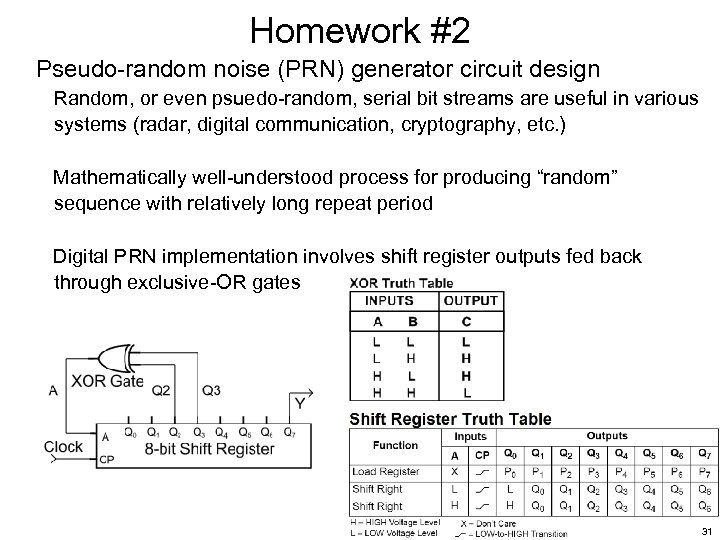 Homework #2 Pseudo-random noise (PRN) generator circuit design Random, or even psuedo-random, serial bit streams are useful in various systems (radar, digital communication, cryptography, etc. ) Mathematically well-understood process for producing “random” sequence with relatively long repeat period Digital PRN implementation involves shift register outputs fed back through exclusive-OR gates 31
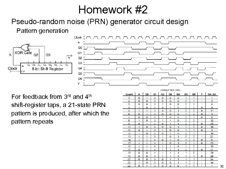 Homework #2 Pseudo-random noise (PRN) generator circuit design Pattern generation For feedback from 3 rd and 4 th shift-register taps, a 21 -state PRN pattern is produced, after which the pattern repeats 32
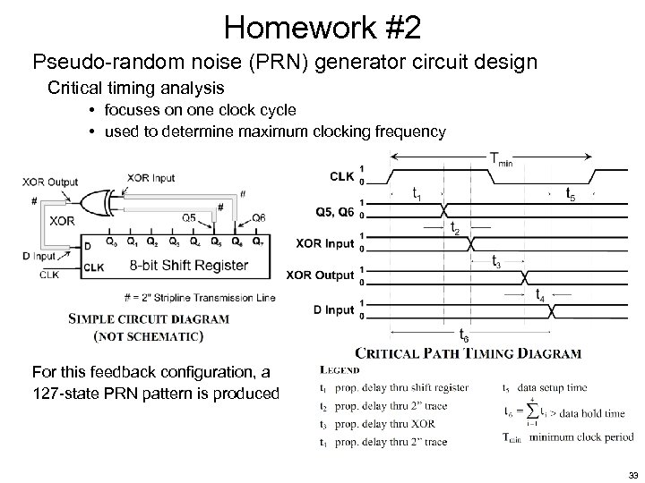 Homework #2 Pseudo-random noise (PRN) generator circuit design Critical timing analysis • focuses on one clock cycle • used to determine maximum clocking frequency For this feedback configuration, a 127 -state PRN pattern is produced 33
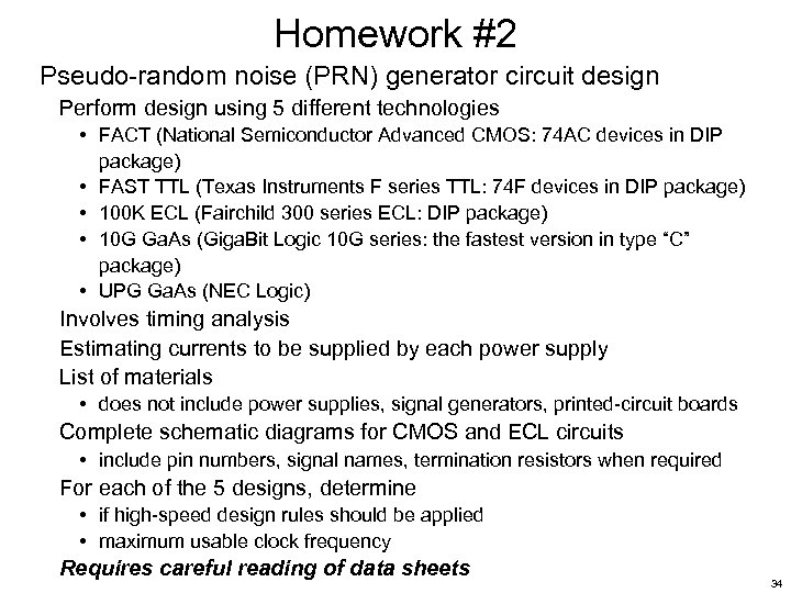 Homework #2 Pseudo-random noise (PRN) generator circuit design Perform design using 5 different technologies • FACT (National Semiconductor Advanced CMOS: 74 AC devices in DIP package) • FAST TTL (Texas Instruments F series TTL: 74 F devices in DIP package) • 100 K ECL (Fairchild 300 series ECL: DIP package) • 10 G Ga. As (Giga. Bit Logic 10 G series: the fastest version in type “C” package) • UPG Ga. As (NEC Logic) Involves timing analysis Estimating currents to be supplied by each power supply List of materials • does not include power supplies, signal generators, printed-circuit boards Complete schematic diagrams for CMOS and ECL circuits • include pin numbers, signal names, termination resistors when required For each of the 5 designs, determine • if high-speed design rules should be applied • maximum usable clock frequency Requires careful reading of data sheets 34
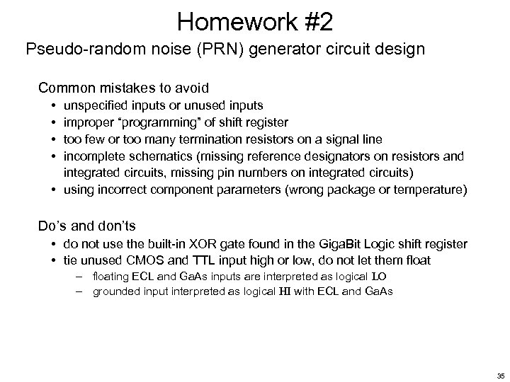 Homework #2 Pseudo-random noise (PRN) generator circuit design Common mistakes to avoid • • unspecified inputs or unused inputs improper “programming” of shift register too few or too many termination resistors on a signal line incomplete schematics (missing reference designators on resistors and integrated circuits, missing pin numbers on integrated circuits) • using incorrect component parameters (wrong package or temperature) Do’s and don’ts • do not use the built-in XOR gate found in the Giga. Bit Logic shift register • tie unused CMOS and TTL input high or low, do not let them float – floating ECL and Ga. As inputs are interpreted as logical LO – grounded input interpreted as logical HI with ECL and Ga. As 35
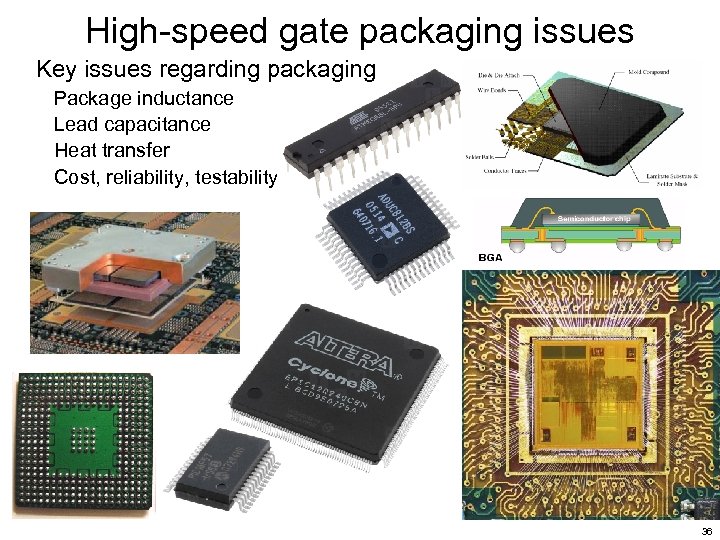 High-speed gate packaging issues Key issues regarding packaging Package inductance Lead capacitance Heat transfer Cost, reliability, testability 36
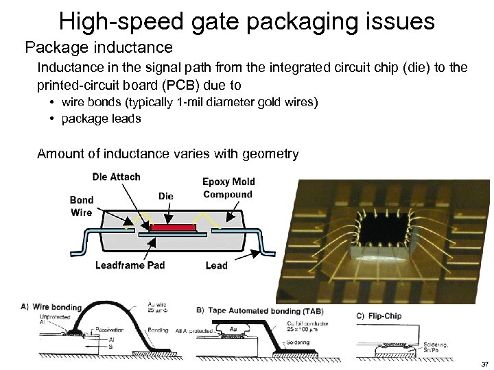 High-speed gate packaging issues Package inductance Inductance in the signal path from the integrated circuit chip (die) to the printed-circuit board (PCB) due to • wire bonds (typically 1 -mil diameter gold wires) • package leads Amount of inductance varies with geometry 37
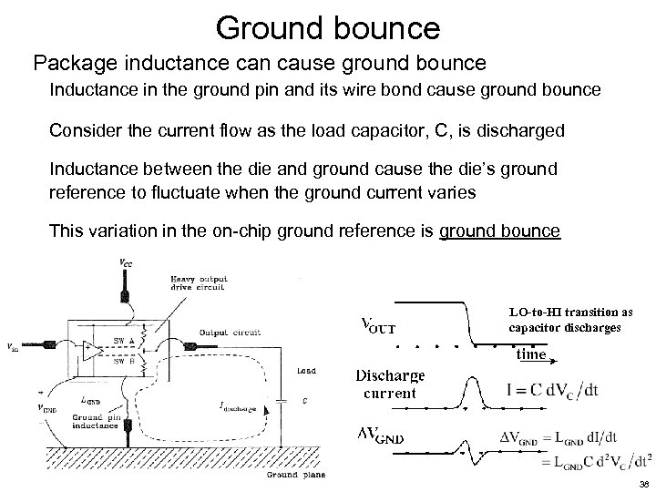 Ground bounce Package inductance can cause ground bounce Inductance in the ground pin and its wire bond cause ground bounce Consider the current flow as the load capacitor, C, is discharged Inductance between the die and ground cause the die’s ground reference to fluctuate when the ground current varies This variation in the on-chip ground reference is ground bounce LO-to-HI transition as capacitor discharges 38
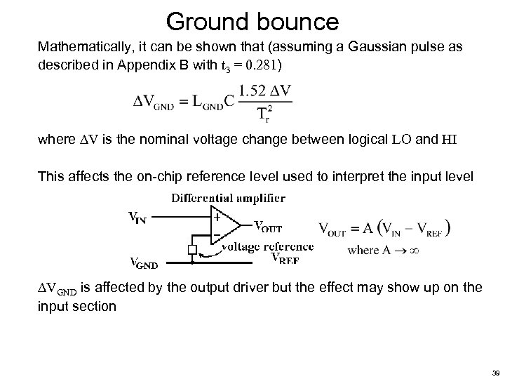 Ground bounce Mathematically, it can be shown that (assuming a Gaussian pulse as described in Appendix B with t 3 = 0. 281) where V is the nominal voltage change between logical LO and HI This affects the on-chip reference level used to interpret the input level VGND is affected by the output driver but the effect may show up on the input section 39
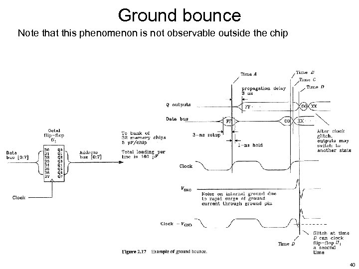 Ground bounce Note that this phenomenon is not observable outside the chip 40
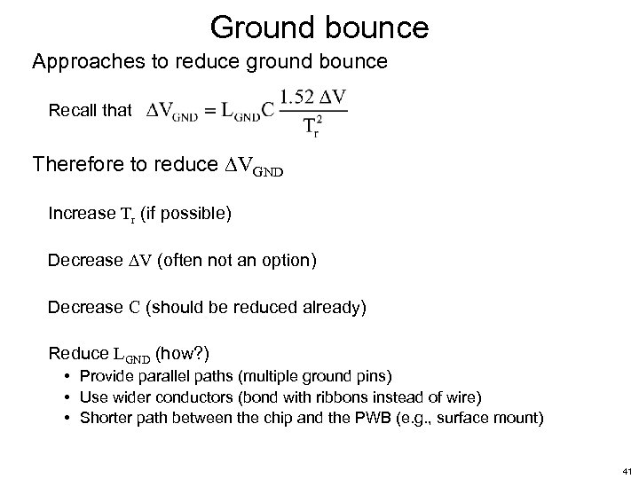 Ground bounce Approaches to reduce ground bounce Recall that Therefore to reduce VGND Increase Tr (if possible) Decrease V (often not an option) Decrease C (should be reduced already) Reduce LGND (how? ) • Provide parallel paths (multiple ground pins) • Use wider conductors (bond with ribbons instead of wire) • Shorter path between the chip and the PWB (e. g. , surface mount) 41
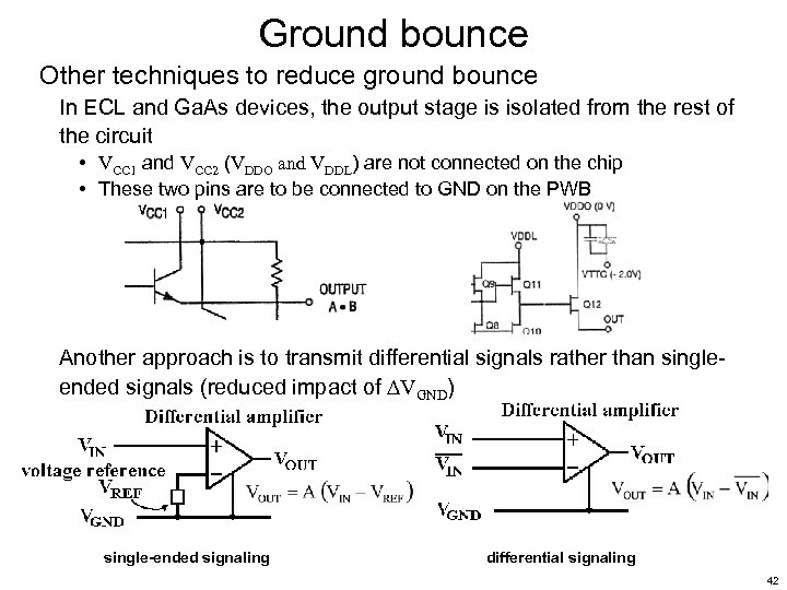 Ground bounce Other techniques to reduce ground bounce In ECL and Ga. As devices, the output stage is isolated from the rest of the circuit • VCC 1 and VCC 2 (VDDO and VDDL) are not connected on the chip • These two pins are to be connected to GND on the PWB Another approach is to transmit differential signals rather than singleended signals (reduced impact of VGND) single-ended signaling differential signaling 42
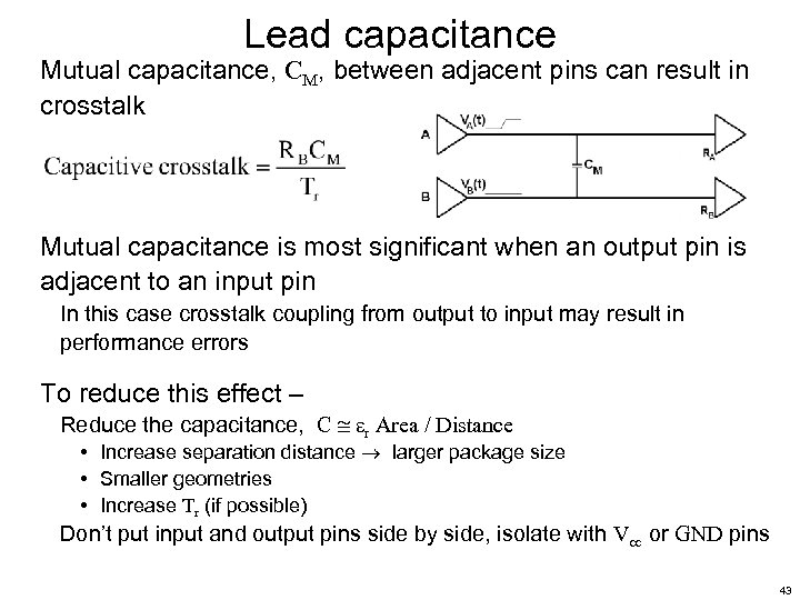 Lead capacitance Mutual capacitance, CM, between adjacent pins can result in crosstalk Mutual capacitance is most significant when an output pin is adjacent to an input pin In this case crosstalk coupling from output to input may result in performance errors To reduce this effect – Reduce the capacitance, C r Area / Distance • Increase separation distance larger package size • Smaller geometries • Increase Tr (if possible) Don’t put input and output pins side by side, isolate with Vcc or GND pins 43
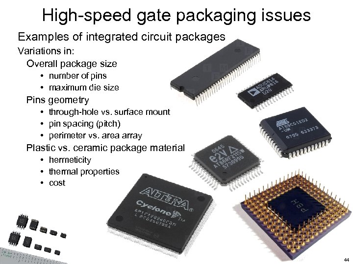 High-speed gate packaging issues Examples of integrated circuit packages Variations in: Overall package size • number of pins • maximum die size Pins geometry • through-hole vs. surface mount • pin spacing (pitch) • perimeter vs. area array Plastic vs. ceramic package material • hermeticity • thermal properties • cost 44
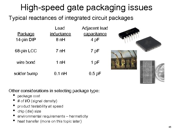 High-speed gate packaging issues Typical reactances of integrated circuit packages Package 14 -pin DIP Lead inductance 8 n. H Adjacent lead capacitance 4 p. F 68 -pin LCC 7 n. H 7 p. F wire bond 1 n. H 1 p. F solder bump 0. 1 n. H 0. 5 p. F Other considerations in selecting package type: • • • package cost # of I/O (signal density) product testability at speed chip (die) size environmental requirements – hermeticity heat transfer (more on this topic later) 45
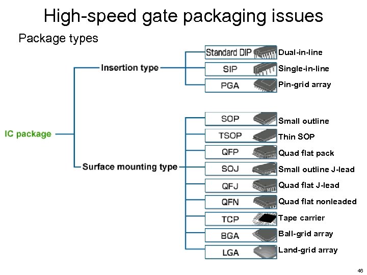 High-speed gate packaging issues Package types Dual-in-line Single-in-line Pin-grid array Small outline Thin SOP Quad flat pack Small outline J-lead Quad flat nonleaded Tape carrier Ball-grid array Land-grid array 46
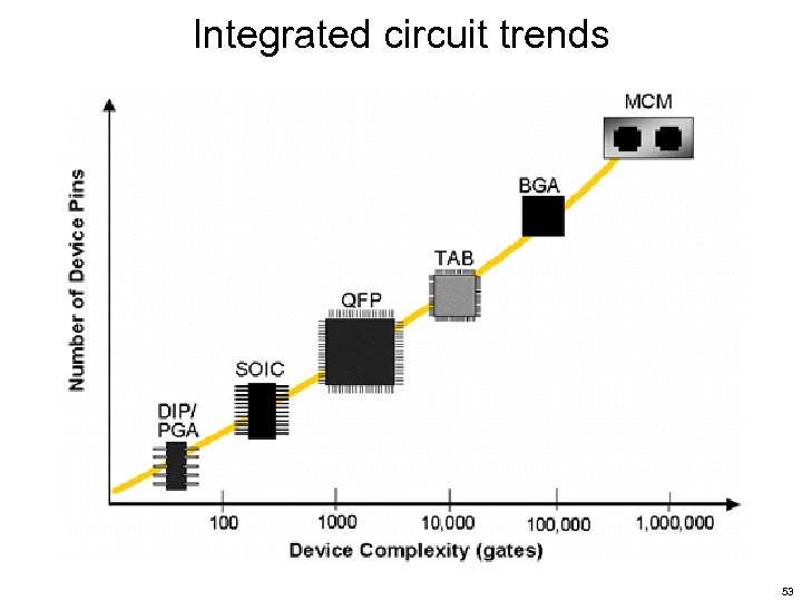
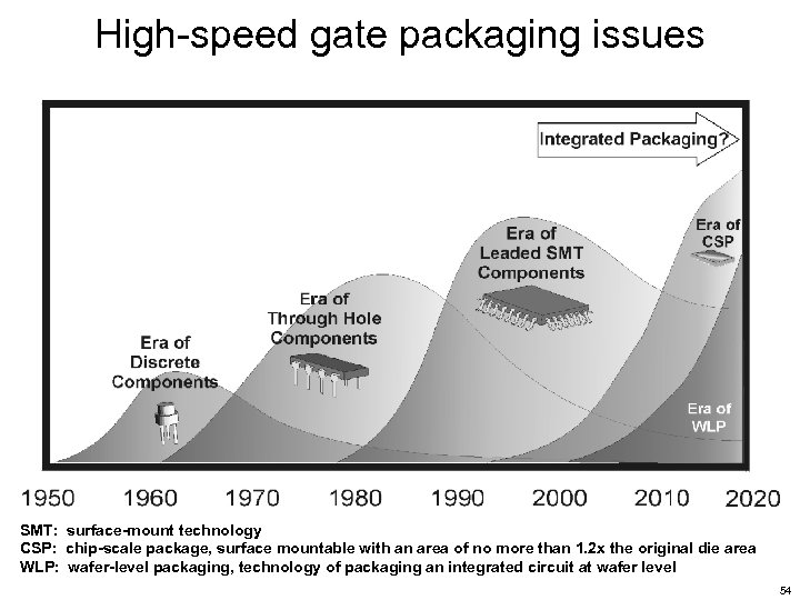
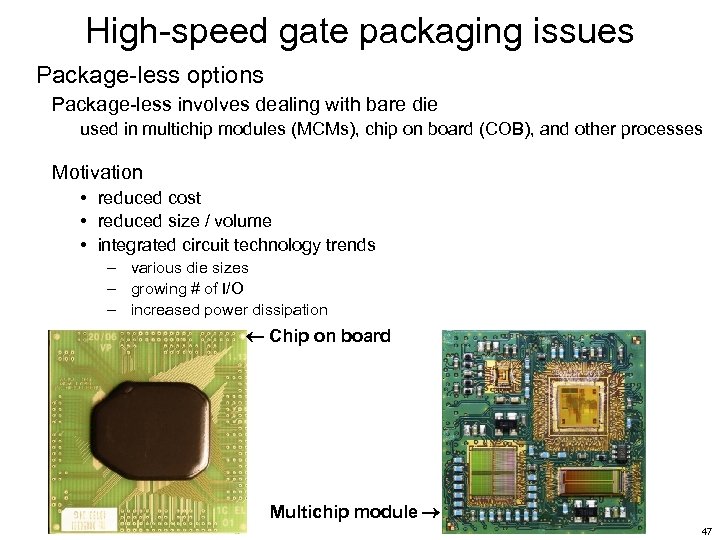 High-speed gate packaging issues Package-less options Package-less involves dealing with bare die used in multichip modules (MCMs), chip on board (COB), and other processes Motivation • reduced cost • reduced size / volume • integrated circuit technology trends – various die sizes – growing # of I/O – increased power dissipation Chip on board Multichip module 47
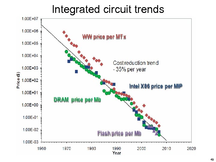
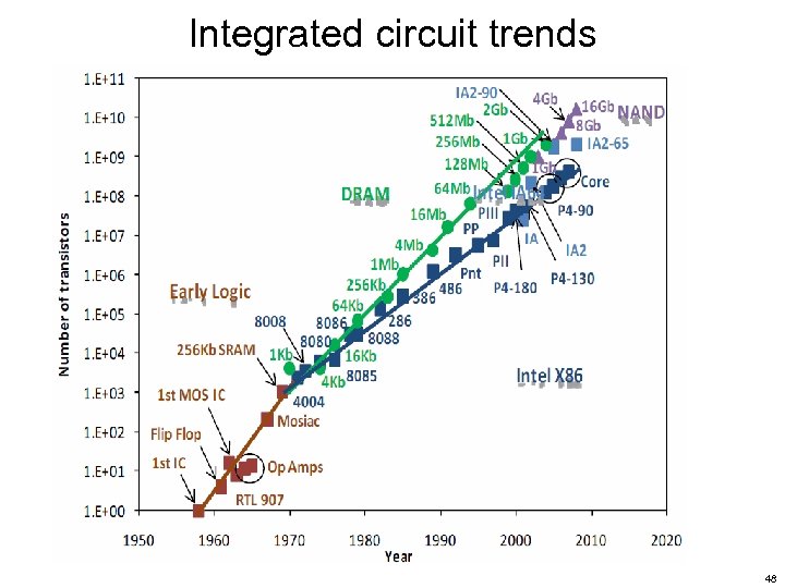 Integrated circuit trends 48
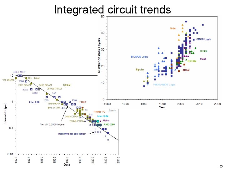
 Integrated circuit trends 49
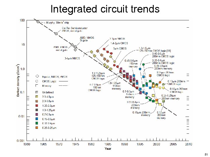
 Integrated circuit trends 50
 Integrated circuit trends 51
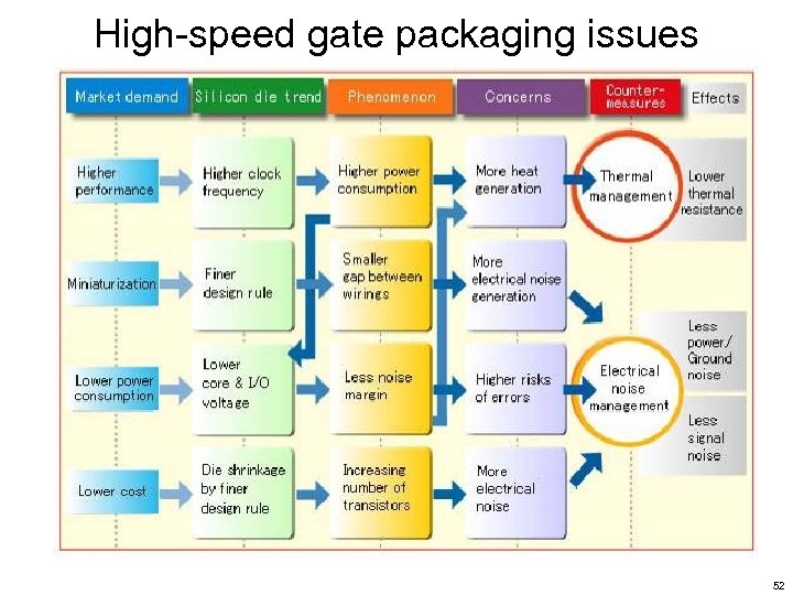 High-speed gate packaging issues 52
 Integrated circuit trends 53
 High-speed gate packaging issues SMT: surface-mount technology CSP: chip-scale package, surface mountable with an area of no more than 1. 2 x the original die area WLP: wafer-level packaging, technology of packaging an integrated circuit at wafer level 54
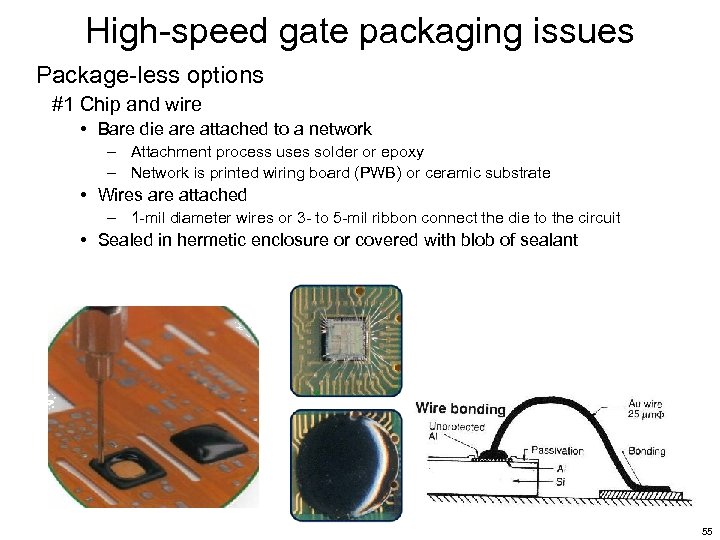 High-speed gate packaging issues Package-less options #1 Chip and wire • Bare die are attached to a network – Attachment process uses solder or epoxy – Network is printed wiring board (PWB) or ceramic substrate • Wires are attached – 1 -mil diameter wires or 3 - to 5 -mil ribbon connect the die to the circuit • Sealed in hermetic enclosure or covered with blob of sealant 55
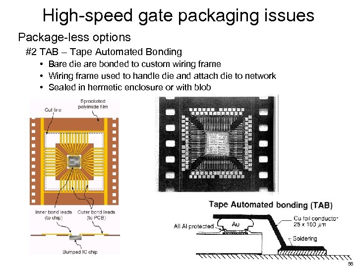 High-speed gate packaging issues Package-less options #2 TAB – Tape Automated Bonding • Bare die are bonded to custom wiring frame • Wiring frame used to handle die and attach die to network • Sealed in hermetic enclosure or with blob 56
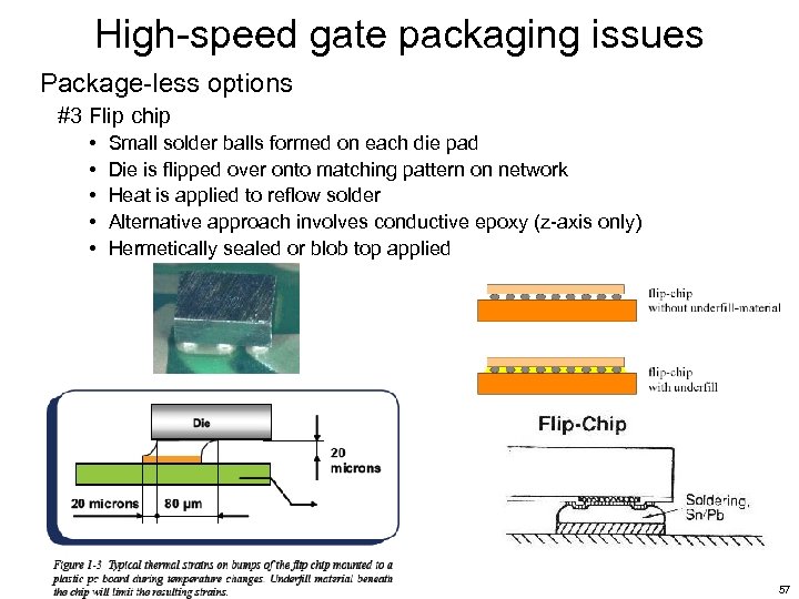 High-speed gate packaging issues Package-less options #3 Flip chip • • • Small solder balls formed on each die pad Die is flipped over onto matching pattern on network Heat is applied to reflow solder Alternative approach involves conductive epoxy (z-axis only) Hermetically sealed or blob top applied 57
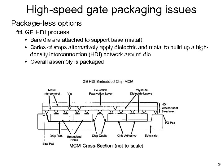 High-speed gate packaging issues Package-less options #4 GE HDI process • Bare die are attached to support base (metal) • Series of steps alternatively apply dielectric and metal to build up a highdensity interconnection (HDI) network around die • Overall assembly is packaged 58
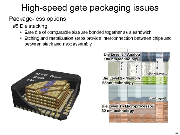 High-speed gate packaging issues Package-less options #5 Die stacking • Bare die of comparable size are bonded together as a sandwich • Etching and metalization steps provide interconnection between chips and between stack and next assembly 59
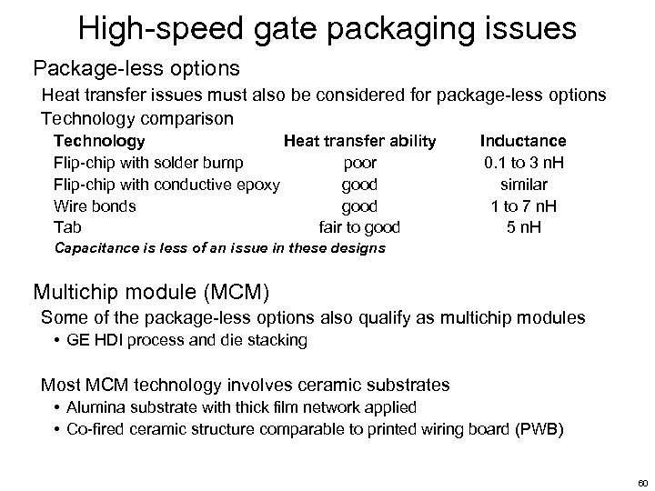 High-speed gate packaging issues Package-less options Heat transfer issues must also be considered for package-less options Technology comparison Technology Heat transfer ability Flip-chip with solder bump poor Flip-chip with conductive epoxy good Wire bonds good Tab fair to good Inductance 0. 1 to 3 n. H similar 1 to 7 n. H 5 n. H Capacitance is less of an issue in these designs Multichip module (MCM) Some of the package-less options also qualify as multichip modules • GE HDI process and die stacking Most MCM technology involves ceramic substrates • Alumina substrate with thick film network applied • Co-fired ceramic structure comparable to printed wiring board (PWB) 60
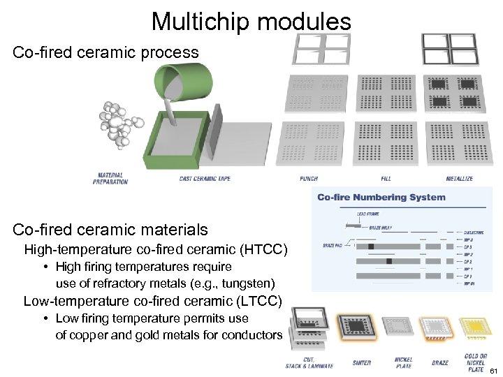 Multichip modules Co-fired ceramic process Co-fired ceramic materials High-temperature co-fired ceramic (HTCC) • High firing temperatures require use of refractory metals (e. g. , tungsten) Low-temperature co-fired ceramic (LTCC) • Low firing temperature permits use of copper and gold metals for conductors 61
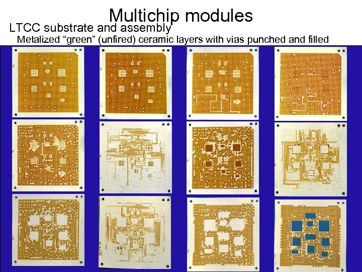 Multichip modules LTCC substrate and assembly Metalized “green” (unfired) ceramic layers with vias punched and filled 62
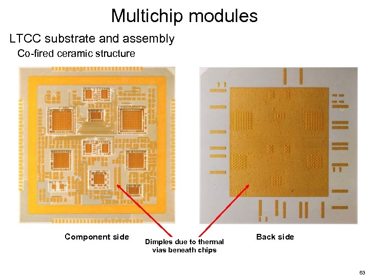 Multichip modules LTCC substrate and assembly Co-fired ceramic structure Component side Dimples due to thermal vias beneath chips Back side 63
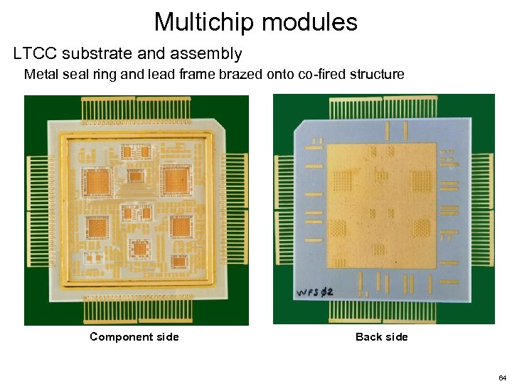 Multichip modules LTCC substrate and assembly Metal seal ring and lead frame brazed onto co-fired structure Component side Back side 64
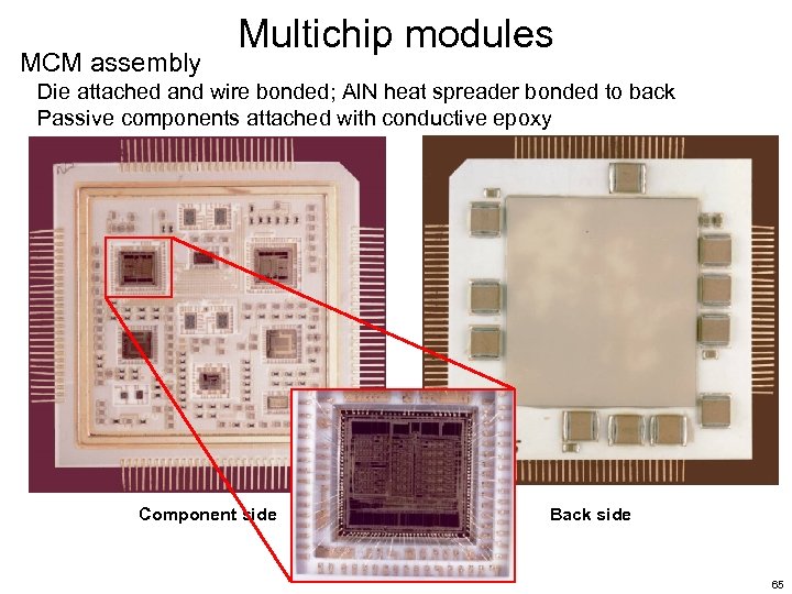 MCM assembly Multichip modules Die attached and wire bonded; Al. N heat spreader bonded to back Passive components attached with conductive epoxy Component side Back side 65
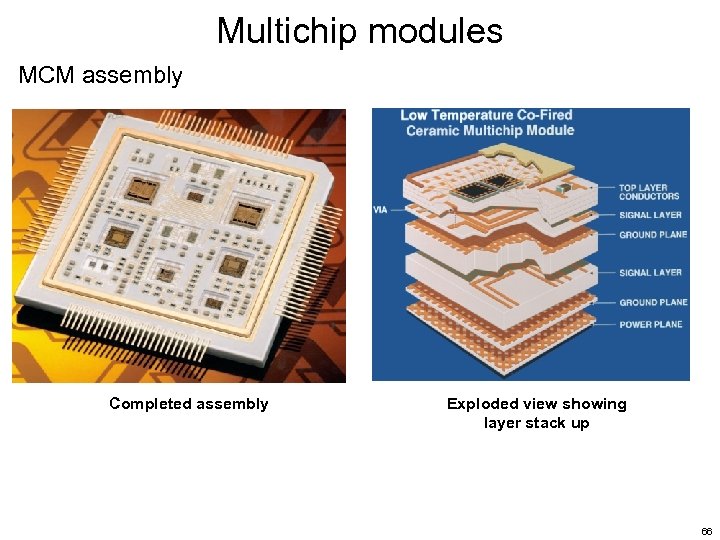 Multichip modules MCM assembly Completed assembly Exploded view showing layer stack up 66
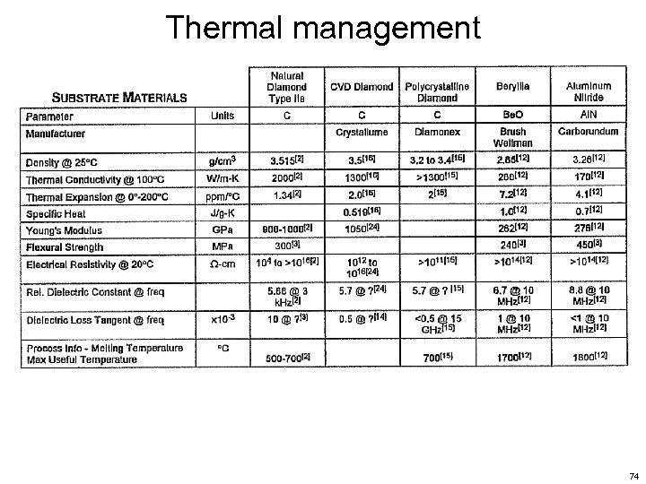
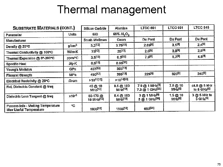
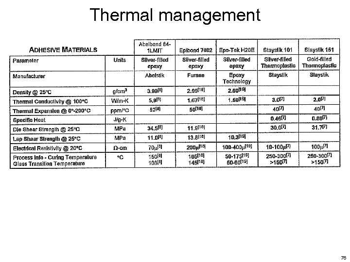
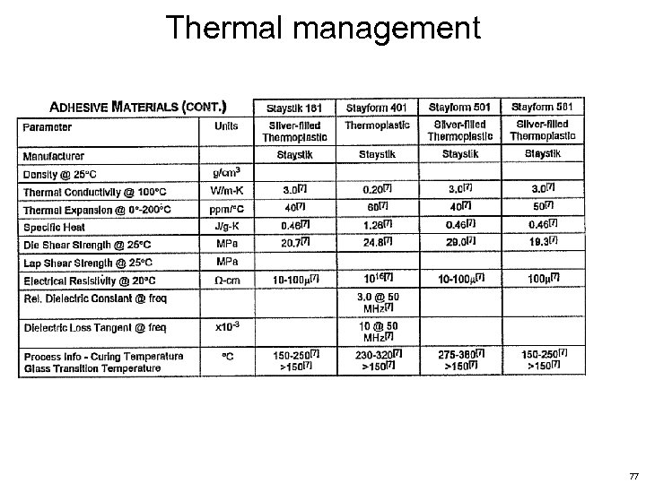
 High-speed gate packaging issues Thermal management Electronic devices dissipate power, PD This power is released as heat Due to thermal resistance, the heat results in a temperature increase Elevated temperatures cause problems for at least two reasons #1 Thermal expansion • Materials expand with increasing temperature • Different materials expand at different rates • Dissimilar materials that are mechanically connected experience mechanical stress when the temperature changes (increase or decrease) • Temperature cycling results in mechanical fatigue • Mechanical failure can result Also, non-uniform temperature in a solid can result in internal stresses fatigue failure Also, non-uniform temperature in a circuit can change electrical parameters e. g. , threshold voltages in FETs 67
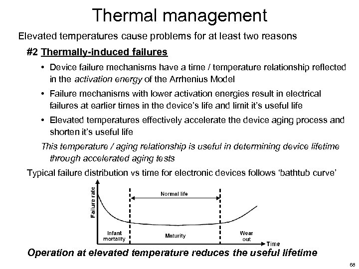 Thermal management Elevated temperatures cause problems for at least two reasons #2 Thermally-induced failures • Device failure mechanisms have a time / temperature relationship reflected in the activation energy of the Arrhenius Model • Failure mechanisms with lower activation energies result in electrical failures at earlier times in the device’s life and limit it’s useful life • Elevated temperatures effectively accelerate the device aging process and shorten it’s useful life This temperature / aging relationship is useful in determining device lifetime through accelerated aging tests Typical failure distribution vs time for electronic devices follows ‘bathtub curve’ Operation at elevated temperature reduces the useful lifetime 68
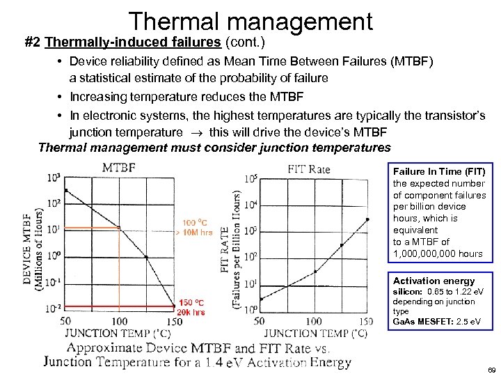 Thermal management #2 Thermally-induced failures (cont. ) • Device reliability defined as Mean Time Between Failures (MTBF) a statistical estimate of the probability of failure • Increasing temperature reduces the MTBF • In electronic systems, the highest temperatures are typically the transistor’s junction temperature this will drive the device’s MTBF Thermal management must consider junction temperatures Failure In Time (FIT) the expected number of component failures per billion device hours, which is equivalent to a MTBF of 1, 000, 000 hours Activation energy silicon: 0. 65 to 1. 22 e. V depending on junction type Ga. As MESFET: 2. 5 e. V 69
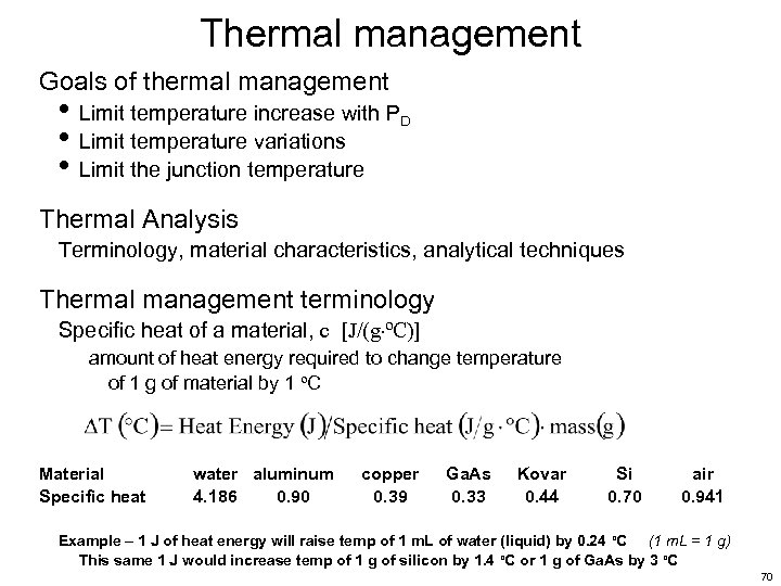 Thermal management Goals of thermal management • Limit temperature increase with PD • Limit temperature variations • Limit the junction temperature Thermal Analysis Terminology, material characteristics, analytical techniques Thermal management terminology Specific heat of a material, c [J/(g ºC)] amount of heat energy required to change temperature of 1 g of material by 1 ºC Material Specific heat water aluminum 4. 186 0. 90 copper 0. 39 Ga. As 0. 33 Kovar 0. 44 Si 0. 70 air 0. 941 Example – 1 J of heat energy will raise temp of 1 m. L of water (liquid) by 0. 24 ºC (1 m. L = 1 g) This same 1 J would increase temp of 1 g of silicon by 1. 4 ºC or 1 g of Ga. As by 3 ºC 70
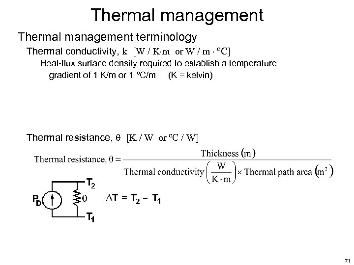 Thermal management terminology Thermal conductivity, k [W / K m or W / m ºC] Heat-flux surface density required to establish a temperature gradient of 1 K/m or 1 ºC/m (K = kelvin) Thermal resistance, [K / W or ºC / W] 71
![Thermal management terminology Coefficient of thermal expansion, CTE [ppm / ºC] Dimension change for Thermal management terminology Coefficient of thermal expansion, CTE [ppm / ºC] Dimension change for](https://present5.com/presentation/a4fd2d87eaf072c342666090468f8479/image-72.jpg) Thermal management terminology Coefficient of thermal expansion, CTE [ppm / ºC] Dimension change for T of 1 ºC Usually specified at a given temperature Heat sink Sink for heat with essentially constant temperature examples: the ocean, Antarctic ice sheet Heat spreader or heat pipe Good thermal conductor ( T 0) but limited heat capacity Used to transfer or distribute heat 72
Thermal management terminology Coefficient of thermal expansion, CTE [ppm / ºC] Dimension change for T of 1 ºC Usually specified at a given temperature Heat sink Sink for heat with essentially constant temperature examples: the ocean, Antarctic ice sheet Heat spreader or heat pipe Good thermal conductor ( T 0) but limited heat capacity Used to transfer or distribute heat 72
 Thermal management 73
 Thermal management 74
 Thermal management 75
 Thermal management 76
 Thermal management 77
 Thermal management 78
 Thermal management 79
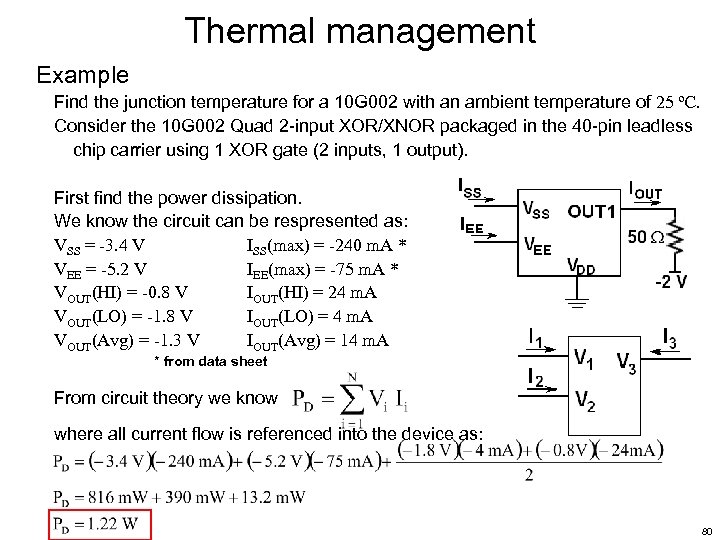 Thermal management Example Find the junction temperature for a 10 G 002 with an ambient temperature of 25 ºC. Consider the 10 G 002 Quad 2 -input XOR/XNOR packaged in the 40 -pin leadless chip carrier using 1 XOR gate (2 inputs, 1 output). First find the power dissipation. We know the circuit can be respresented as: VSS = -3. 4 V ISS(max) = -240 m. A * VEE = -5. 2 V IEE(max) = -75 m. A * VOUT(HI) = -0. 8 V IOUT(HI) = 24 m. A VOUT(LO) = -1. 8 V IOUT(LO) = 4 m. A VOUT(Avg) = -1. 3 V IOUT(Avg) = 14 m. A * from data sheet From circuit theory we know where all current flow is referenced into the device as: 80
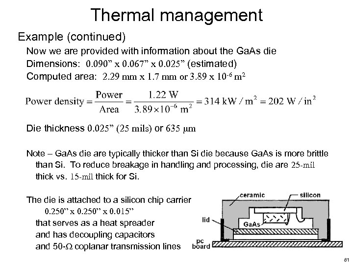 Thermal management Example (continued) Now we are provided with information about the Ga. As die Dimensions: 0. 090” x 0. 067” x 0. 025” (estimated) Computed area: 2. 29 mm x 1. 7 mm or 3. 89 x 10 -6 m 2 Die thickness 0. 025” (25 mils) or 635 m Note – Ga. As die are typically thicker than Si die because Ga. As is more brittle than Si. To reduce breakage in handling and processing, die are 25 -mil thick vs. 15 -mil thick for Si. The die is attached to a silicon chip carrier 0. 250” x 0. 015” that serves as a heat spreader and has decoupling capacitors and 50 - coplanar transmission lines 81
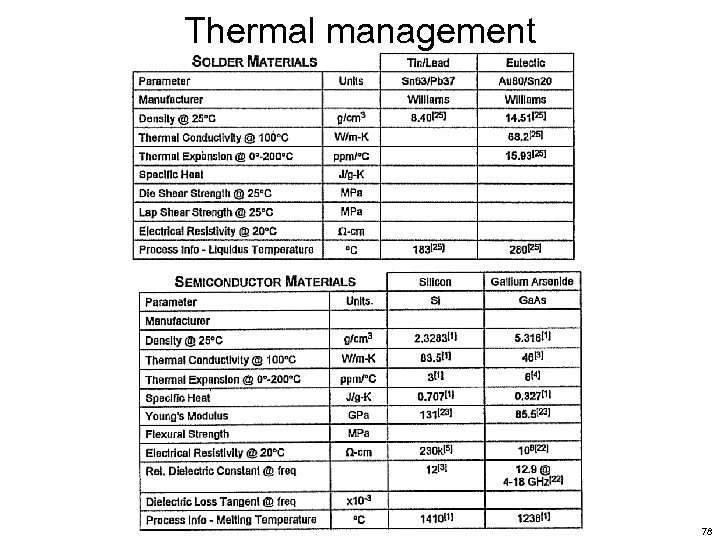
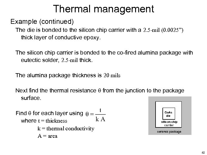 Thermal management Example (continued) The die is bonded to the silicon chip carrier with a 2. 5 -mil (0. 0025”) thick layer of conductive epoxy. The silicon chip carrier is bonded to the co-fired alumina package with eutectic solder, 2. 5 -mil thick. The alumina package thickness is 20 mils Next find thermal resistance from the junction to the package surface. Find for each layer using where t = thickness k = thermal conductivity A = area 82
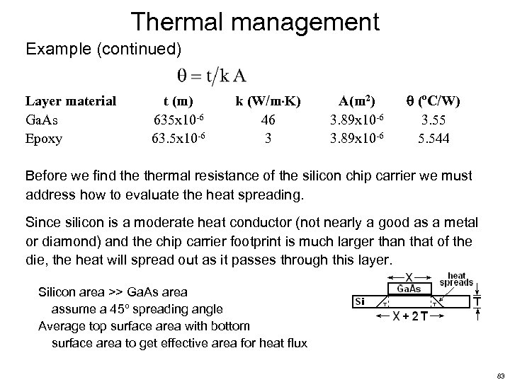 Thermal management Example (continued) Layer material Ga. As Epoxy t (m) 635 x 10 -6 63. 5 x 10 -6 k (W/m K) 46 3 A(m 2) 3. 89 x 10 -6 (ºC/W) 3. 55 5. 544 Before we find thermal resistance of the silicon chip carrier we must address how to evaluate the heat spreading. Since silicon is a moderate heat conductor (not nearly a good as a metal or diamond) and the chip carrier footprint is much larger than that of the die, the heat will spread out as it passes through this layer. Silicon area >> Ga. As area assume a 45º spreading angle Average top surface area with bottom surface area to get effective area for heat flux 83
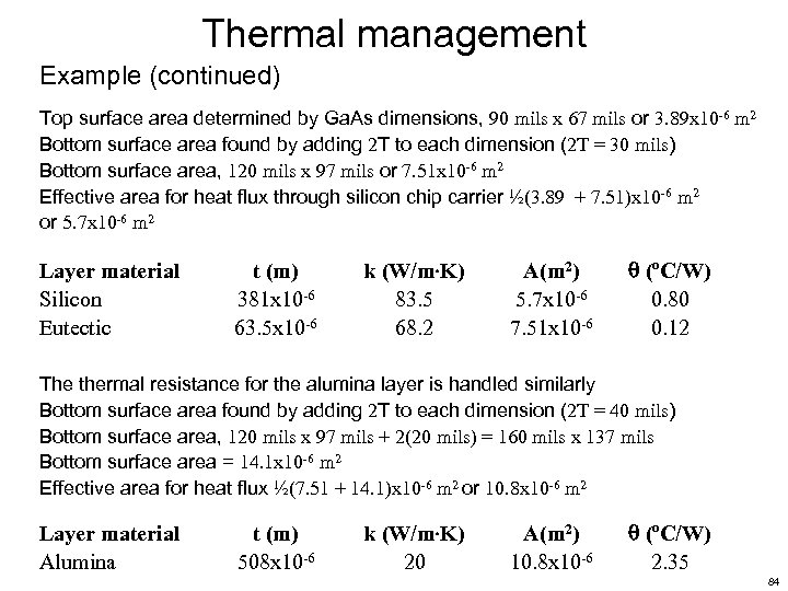 Thermal management Example (continued) Top surface area determined by Ga. As dimensions, 90 mils x 67 mils or 3. 89 x 10 -6 m 2 Bottom surface area found by adding 2 T to each dimension (2 T = 30 mils) Bottom surface area, 120 mils x 97 mils or 7. 51 x 10 -6 m 2 Effective area for heat flux through silicon chip carrier ½(3. 89 + 7. 51)x 10 -6 m 2 or 5. 7 x 10 -6 m 2 Layer material Silicon Eutectic t (m) 381 x 10 -6 63. 5 x 10 -6 k (W/m K) 83. 5 68. 2 A(m 2) 5. 7 x 10 -6 7. 51 x 10 -6 (ºC/W) 0. 80 0. 12 The thermal resistance for the alumina layer is handled similarly Bottom surface area found by adding 2 T to each dimension (2 T = 40 mils) Bottom surface area, 120 mils x 97 mils + 2(20 mils) = 160 mils x 137 mils Bottom surface area = 14. 1 x 10 -6 m 2 Effective area for heat flux ½(7. 51 + 14. 1)x 10 -6 m 2 or 10. 8 x 10 -6 m 2 Layer material Alumina t (m) 508 x 10 -6 k (W/m K) 20 A(m 2) 10. 8 x 10 -6 (ºC/W) 2. 35 84
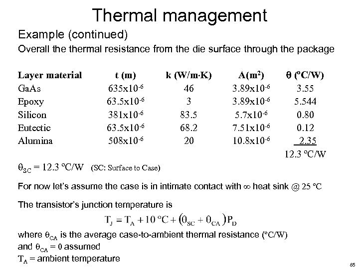 Thermal management Example (continued) Overall thermal resistance from the die surface through the package Layer material Ga. As Epoxy Silicon Eutectic Alumina t (m) 635 x 10 -6 63. 5 x 10 -6 381 x 10 -6 63. 5 x 10 -6 508 x 10 -6 SC = 12. 3 ºC/W k (W/m K) 46 3 83. 5 68. 2 20 A(m 2) 3. 89 x 10 -6 5. 7 x 10 -6 7. 51 x 10 -6 10. 8 x 10 -6 (ºC/W) 3. 55 5. 544 0. 80 0. 12 2. 35 12. 3 ºC/W (SC: Surface to Case) For now let’s assume the case is in intimate contact with heat sink @ 25 ºC The transistor’s junction temperature is where CA is the average case-to-ambient thermal resistance (ºC/W) and CA = 0 assumed TA = ambient temperature 85
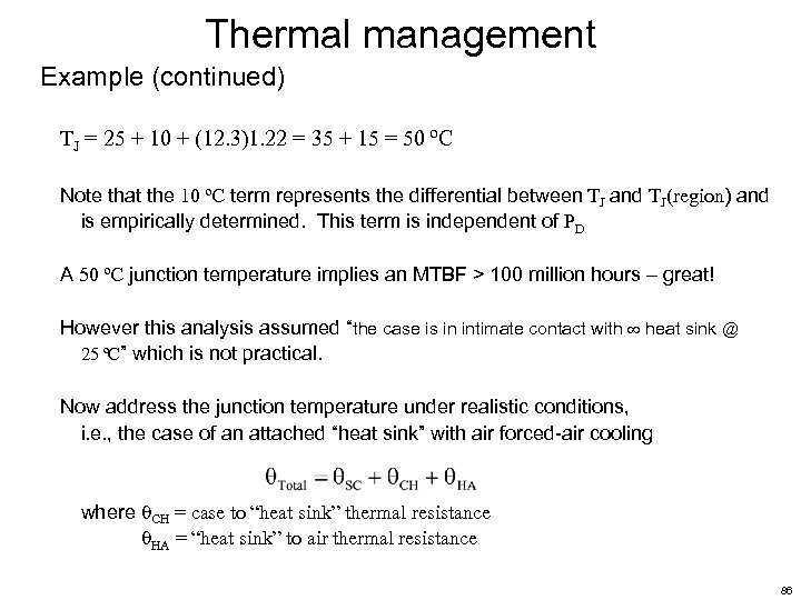 Thermal management Example (continued) TJ = 25 + 10 + (12. 3)1. 22 = 35 + 15 = 50 ºC Note that the 10 ºC term represents the differential between TJ and TJ(region) and is empirically determined. This term is independent of PD A 50 ºC junction temperature implies an MTBF > 100 million hours – great! However this analysis assumed “the case is in intimate contact with heat sink @ 25 ºC” which is not practical. Now address the junction temperature under realistic conditions, i. e. , the case of an attached “heat sink” with air forced-air cooling where CH = case to “heat sink” thermal resistance HA = “heat sink” to air thermal resistance 86
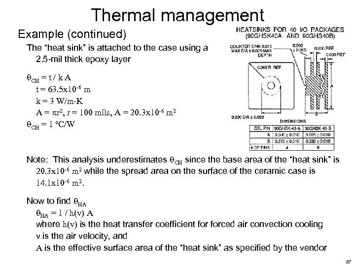 Thermal management Example (continued) The “heat sink” is attached to the case using a 2. 5 -mil thick epoxy layer CH = t / k A t = 63. 5 x 10 -6 m k = 3 W/m K A = r 2, r = 100 mils, A = 20. 3 x 10 -6 m 2 CH = 1 ºC/W Note: This analysis underestimates CH since the base area of the “heat sink” is 20. 3 x 10 -6 m 2 while the spread area on the surface of the ceramic case is 14. 1 x 10 -6 m 2. Now to find HA HA = 1 / h(v) A where h(v) is the heat transfer coefficient forced air convection cooling v is the air velocity, and A is the effective surface area of the “heat sink” as specified by the vendor 87
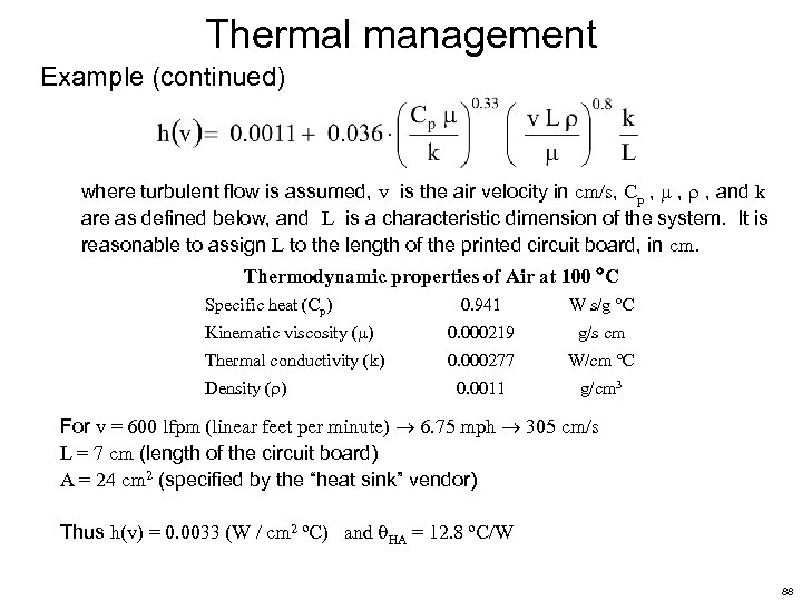 Thermal management Example (continued) where turbulent flow is assumed, v is the air velocity in cm/s, Cp , , , and k are as defined below, and L is a characteristic dimension of the system. It is reasonable to assign L to the length of the printed circuit board, in cm. Thermodynamic properties of Air at 100 C 0. 941 W s/g C Kinematic viscosity ( ) 0. 000219 g/s cm Thermal conductivity (k) 0. 000277 W/cm C 0. 0011 g/cm 3 Specific heat (Cp) Density ( ) For v = 600 lfpm (linear feet per minute) 6. 75 mph 305 cm/s L = 7 cm (length of the circuit board) A = 24 cm 2 (specified by the “heat sink” vendor) Thus h(v) = 0. 0033 (W / cm 2 ºC) and HA = 12. 8 ºC/W 88
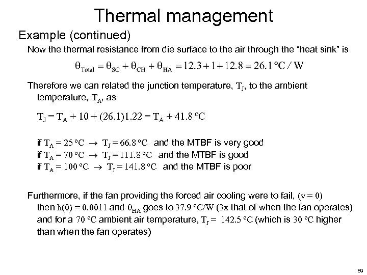 Thermal management Example (continued) Now thermal resistance from die surface to the air through the “heat sink” is Therefore we can related the junction temperature, TJ, to the ambient temperature, TA, as TJ = TA + 10 + (26. 1)1. 22 = TA + 41. 8 ºC if TA = 25 ºC TJ = 66. 8 ºC and the MTBF is very good if TA = 70 ºC TJ = 111. 8 ºC and the MTBF is good if TA = 100 ºC TJ = 141. 8 ºC and the MTBF is poor Furthermore, if the fan providing the forced air cooling were to fail, (v = 0) then h(0) = 0. 0011 and HA goes to 37. 9 ºC/W (3 x that of when the fan operates) and for a 70 ºC ambient air temperature, TJ = 142. 5 ºC (which is 30 ºC higher than when the fan operates) 89
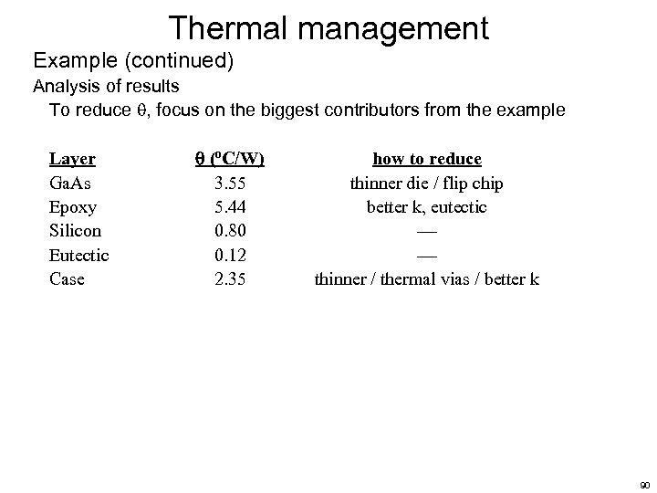 Thermal management Example (continued) Analysis of results To reduce , focus on the biggest contributors from the example Layer Ga. As Epoxy Silicon Eutectic Case (ºC/W) 3. 55 5. 44 0. 80 0. 12 2. 35 how to reduce thinner die / flip chip better k, eutectic thinner / thermal vias / better k 90
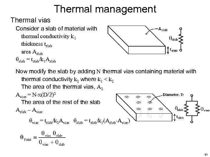 Thermal management Thermal vias Consider a slab of material with thermal conductivity k 1 thickness tslab area Aslab = tslab/k 1 Aslab Now modify the slab by adding N thermal vias containing material with thermal conductivity k 2 where k 1 < k 2 The area of thermal vias, A 2 Avias = N (D/2)2 The area of the rest of the slab Aslab – Avias = tslab/k 2 Avias slab = tslab/k 1(Aslab-Avias) 91
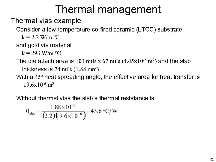 Thermal management Thermal vias example Consider a low-temperature co-fired ceramic (LTCC) substrate k = 2. 2 W/m ºC and gold via material k = 293 W/m ºC The die attach area is 103 mils x 67 mils (4. 45 x 10 -6 m 2) and the slab thickness is 74 mils (1. 88 mm) With a 45º heat spreading angle, the effective area for heat transfer is 19. 6 x 10 -6 m 2 Without thermal vias the slab’s thermal resistance is 92
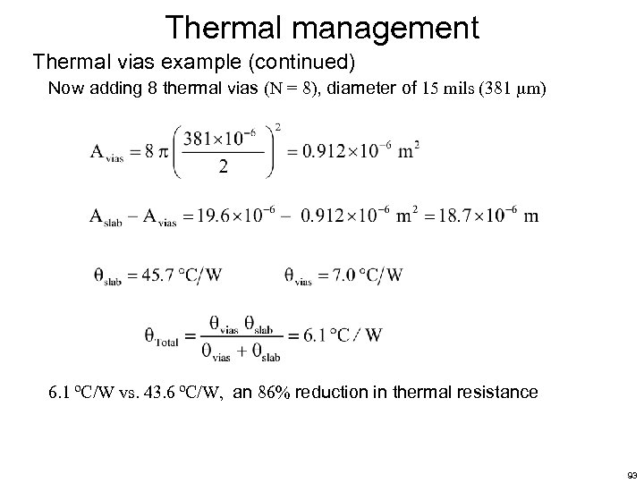 Thermal management Thermal vias example (continued) Now adding 8 thermal vias (N = 8), diameter of 15 mils (381 m) 6. 1 ºC/W vs. 43. 6 ºC/W, an 86% reduction in thermal resistance 93
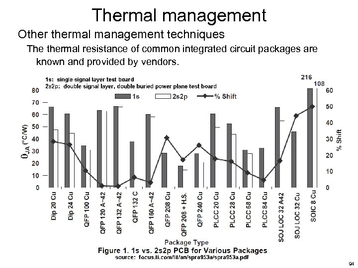 Thermal management Othermal management techniques The thermal resistance of common integrated circuit packages are known and provided by vendors. 94
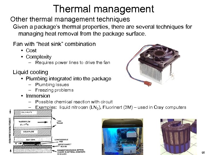 Thermal management Othermal management techniques Given a package’s thermal properties, there are several techniques for managing heat removal from the package surface. Fan with “heat sink” combination • Cost • Complexity – Requires power lines to drive the fan Liquid cooling • Plumbing integrated into the package – Plumbing issues – Freezing problems • Immersion – Possible chemical reaction with circuit – Examples: liquid nitrogen (LN 2), Fluorinert (3 M) – used in Cray computers 95
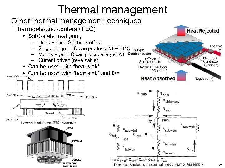 Thermal management Othermal management techniques Thermoelectric coolers (TEC) • Solid-state heat pump – – Uses Peltier–Seebeck effect Single stage TEC can produce T 70 ºC Multi-stage TEC can produce larger T Current driven (reversable) • Can be used with “heat sink” and fan 96
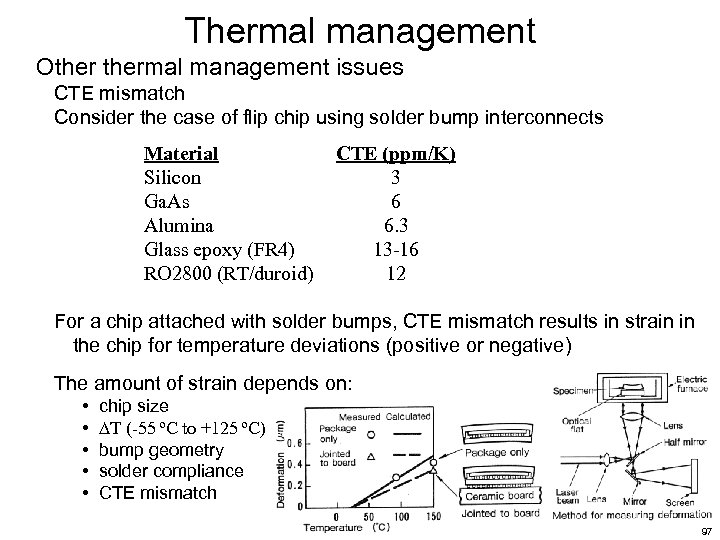 Thermal management Othermal management issues CTE mismatch Consider the case of flip chip using solder bump interconnects Material Silicon Ga. As Alumina Glass epoxy (FR 4) RO 2800 (RT/duroid) CTE (ppm/K) 3 6 6. 3 13 -16 12 For a chip attached with solder bumps, CTE mismatch results in strain in the chip for temperature deviations (positive or negative) The amount of strain depends on: • • • chip size T (-55 ºC to +125 ºC) bump geometry solder compliance CTE mismatch 97
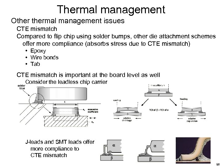 Thermal management Othermal management issues CTE mismatch Compared to flip chip using solder bumps, other die attachment schemes offer more compliance (absorbs stress due to CTE mismatch) • Epoxy • Wire bonds • Tab CTE mismatch is important at the board level as well Consider the leadless chip carrier J-leads and SMT leads offer more compliance to CTE mismatch 98
 Thermal management HW assignment Thermal Resistance and Junction Temperature For each case below, find SC (10 points 3 cases), Tjunction (10 points 3 cases), CH (10 points 1 case), HA (10 points 1 case), where SC = thermal resistance from die surface to case CH = thermal resistance from case to ‘heat sink’ HA = thermal resistance from ‘heat sink’ to air 1. Die – Ga. As, dimensions 122 x 105 x 25 mils, power dissipation, PD = 1. 3 W Die is bonded to a substrate with 2 mil thick epoxy (k = 4 W / m C) Substrate – LTCC 851 48 mil thick, area » die footprint Substrate is bonded to a ‘heat sink’ with 2 mil thick epoxy (k = 4 W / m °C) Heat sink – area 24 cm 2, base is 200 mil diameter Air – temp 35°C, flow rate 200 lfpm. 2. Same as #1 except: Substrate contains thermal vias beneath the die The number of vias, N = 16 Via diameter is 15 mils Vias filled with gold material (k = 293 W / m °C) 3. Same as #1 except: Substrate is Aluminum Nitride (Al. N) and not LTCC 851 (There are no thermal vias) 4. Compare the results found in parts 1 -3 and provide a conclusion. (10 points) See course website for complete assignment details 99


