b07d99a84454e628f6f15dd3b5ef7539.ppt
- Количество слайдов: 67
 High Performance Analog Integrated Circuit Design: The Effect of Device Self. Heating on Design Optimization Ronald L. Carter, Professor Analog Integrated Circuit Design Lab Electrical Engineering Department RLCarter: Analog IC Design with Self Heating The University of Texas at Arlington
 Analog IC Design with Self-Heating Heat Source/Temperature Effects n Thermal Equations/Analogy n Thermal Resistance Models n Effect of Thermal Resistance on Device Biasing n Effect of Thermal Resistance on the Circuit Performance RLCarter: Analog IC n Conclusions/Future Work Design with Self n Heating 2
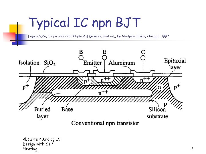 Typical IC npn BJT Figure 9. 2 a, Semiconductor Physics & Devices, 2 nd ed. , by Neamen, Irwin, Chicago, 1997 RLCarter: Analog IC Design with Self Heating 3
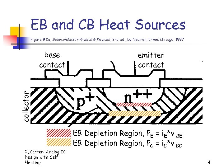 EB and CB Heat Sources Figure 9. 2 a, Semiconductor Physics & Devices, 2 nd ed. , by Neamen, Irwin, Chicago, 1997 emitter contact collector base contact RLCarter: Analog IC Design with Self Heating EB Depletion Region, PE = i. E*v BE EB Depletion Region, PC = i. C*v BC 4
![Temperature Increase Td-Ta=Ta{[1 + (n+1)( e+ c)/Ta)]1/(n+1)1} e and c are pseudo-temperatures via the Temperature Increase Td-Ta=Ta{[1 + (n+1)( e+ c)/Ta)]1/(n+1)1} e and c are pseudo-temperatures via the](https://present5.com/presentation/b07d99a84454e628f6f15dd3b5ef7539/image-5.jpg) Temperature Increase Td-Ta=Ta{[1 + (n+1)( e+ c)/Ta)]1/(n+1)1} e and c are pseudo-temperatures via the Kirchoff transformation, assuming k(T) = k(300 K) [T/300]n n e = RTh, EB |ievbe| n c = RTh, CB |icvbc| n RTh, EB, RTh, CB are thermal res. at Ta. n Following S. H. Whemple, and H. Huang, "Thermal Design of Power Ga. As FETs", in Ga. As FET Principles and RLCarter: Analog ICV. Di. Lorenzo and D. D. Khandelwal, eds. , pp. 313 -347, Artech House, 1982. Technology, J. Design with Self Heating 5
Temperature Increase Td-Ta=Ta{[1 + (n+1)( e+ c)/Ta)]1/(n+1)1} e and c are pseudo-temperatures via the Kirchoff transformation, assuming k(T) = k(300 K) [T/300]n n e = RTh, EB |ievbe| n c = RTh, CB |icvbc| n RTh, EB, RTh, CB are thermal res. at Ta. n Following S. H. Whemple, and H. Huang, "Thermal Design of Power Ga. As FETs", in Ga. As FET Principles and RLCarter: Analog ICV. Di. Lorenzo and D. D. Khandelwal, eds. , pp. 313 -347, Artech House, 1982. Technology, J. Design with Self Heating 5
 Circuit Simulation of Temperature Effects n n n Typically TNOM (parameter spec. temperature) and TEMP (circuit operation temperature) only variables However, Td =Tdevice is a function of ie, vbe, ic and vbc. More flexibility with Vertical Bipolar Inter-Company model (VBIC) RLCarter: Analog IC Design with Self Heating 6
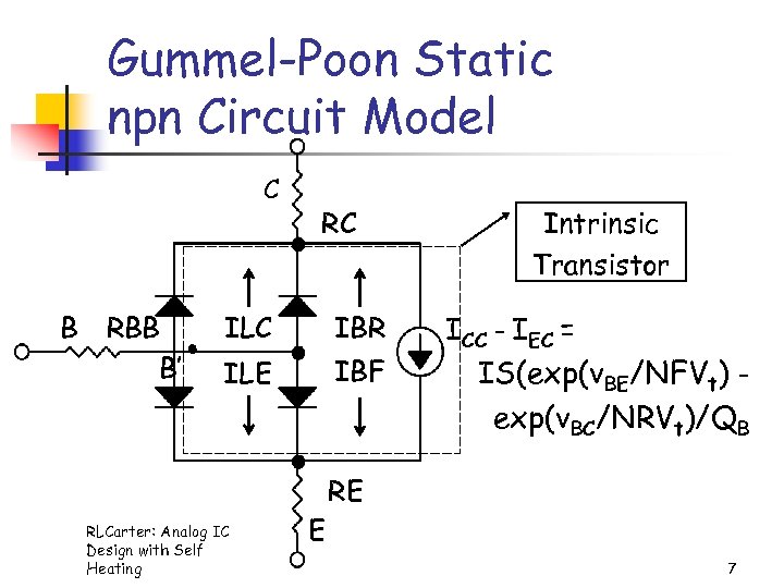 Gummel-Poon Static npn Circuit Model C B RBB B’ RC ILC IBR ILE IBF RLCarter: Analog IC Design with Self Heating E Intrinsic Transistor ICC - IEC = IS(exp(v. BE/NFVt) exp(v. BC/NRVt)/QB RE 7
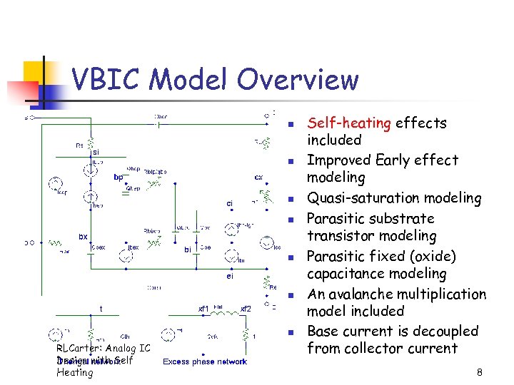 VBIC Model Overview n n n n RLCarter: Analog IC Design with Self Heating Self-heating effects included Improved Early effect modeling Quasi-saturation modeling Parasitic substrate transistor modeling Parasitic fixed (oxide) capacitance modeling An avalanche multiplication model included Base current is decoupled from collector current 8
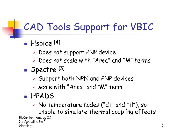 CAD Tools Support for VBIC n Hspice ü ü n Does not support PNP device Does not scale with “Area” and “M” terms Spectre ü ü n [4] [5] Support both NPN and PNP devices scale with “Area” and “M” term HPADS ü No temperature nodes (“dt” and “tl”), so unable to simulate thermal coupling effects RLCarter: Analog IC Design with Self Heating 9
![Temperature Designations for VBIC Parameters Description Spectre [4] Hspice [5] Name Default Temperature rise Temperature Designations for VBIC Parameters Description Spectre [4] Hspice [5] Name Default Temperature rise](https://present5.com/presentation/b07d99a84454e628f6f15dd3b5ef7539/image-10.jpg) Temperature Designations for VBIC Parameters Description Spectre [4] Hspice [5] Name Default Temperature rise of the device from ambient trise 0 dtemp 0 Ambient temperature temp 27 temp 25 Parameters measurement temperature tnom 27 tnom 25 tref 27 RLCarter: Analog IC Design with Self Heating 10
Temperature Designations for VBIC Parameters Description Spectre [4] Hspice [5] Name Default Temperature rise of the device from ambient trise 0 dtemp 0 Ambient temperature temp 27 temp 25 Parameters measurement temperature tnom 27 tnom 25 tref 27 RLCarter: Analog IC Design with Self Heating 10
![Using VBIC in Spectre [5] Name c b e [s] [dt] [tl] Model. Name Using VBIC in Spectre [5] Name c b e [s] [dt] [tl] Model. Name](https://present5.com/presentation/b07d99a84454e628f6f15dd3b5ef7539/image-11.jpg) Using VBIC in Spectre [5] Name c b e [s] [dt] [tl] Model. Name parameter=value. . . n Selft=1 and Rth>0 to enable Self-heating n 1 volt at the temperature nodes = 1 degree in temperature n “tl” node represents the initial local temperature of device which always corresponds to trise+temp n “dt” node represents the rise above trise+temp caused by thermal dissipation, whose value equals V(dt)-V(tl) n RLCarter: Analog IC Device temperature=V(dt)-V(tl)+trise+temp Design with Self Heating 11
Using VBIC in Spectre [5] Name c b e [s] [dt] [tl] Model. Name parameter=value. . . n Selft=1 and Rth>0 to enable Self-heating n 1 volt at the temperature nodes = 1 degree in temperature n “tl” node represents the initial local temperature of device which always corresponds to trise+temp n “dt” node represents the rise above trise+temp caused by thermal dissipation, whose value equals V(dt)-V(tl) n RLCarter: Analog IC Device temperature=V(dt)-V(tl)+trise+temp Design with Self Heating 11
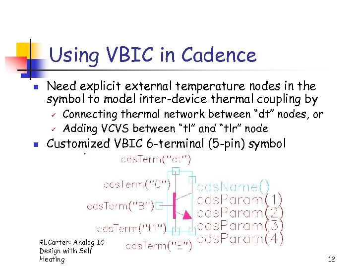 Using VBIC in Cadence n Need explicit external temperature nodes in the symbol to model inter-device thermal coupling by ü ü n Connecting thermal network between “dt” nodes, or Adding VCVS between “tl” and “tlr” node Customized VBIC 6 -terminal (5 -pin) symbol RLCarter: Analog IC Design with Self Heating 12
 Model Conversion n n Most BJTs are defined with SGP model A conversion from SGP to VBIC is needed Only approximate conversion is possible Some parameters are unmapped such as Rth and Cth Two approaches are provided ü ü Manual conversion — done empirically and need Local Ratio Evaluation [2] Program conversion using program sgp_2_vbic [3] RLCarter: Analog IC Design with Self Heating 13
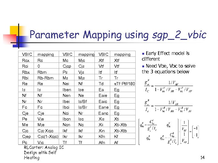 Parameter Mapping using sgp_2_vbic VBIC mapping VBIC Rcx Rc Mc Rci 0 Cjcp Rbx Rbm Ps Rbi Rb-Rbm Ms Re Re Nei Is Is Iben Nf Nf Nen Nr Nr Ibei Fc Fc Ibci Cje Nci Pe Vje Ibcn Me Mje Ncn Cjc·Xcjc Ikf Cjep Cjc(1 -Xcjc) Ikr Pc Vjc Tf RLCarter: Analog IC Design with Self Heating mapping Mjc Cjs Vjs Mjs Nf Ise Ne Is/Bf Is/Br Nr Isc Nc Ikf Ikr Tf VBIC Xtf Vtf Itf Tr Td Ea Eaie Eaic Eane Eanc Xis Xii Xin Kfn Afn mapping Xtf Vtf Itf Tr Tf·Ptf/180 Eg Eg Eg Xti-Xtb Kf Af Early Effect model is different n Need Vbe, Vbc to solve the 3 equations below n 14
 Analog IC Design with Self-Heating Heat Source/Temperature Effects n Thermal Equations/Analogy n Thermal Resistance Models n Effect of Thermal Resistance on Device Biasing n Effect of Thermal Resistance on the Circuit Performance RLCarter: Analog IC n Conclusions/Future Work Design with Self n Heating 15
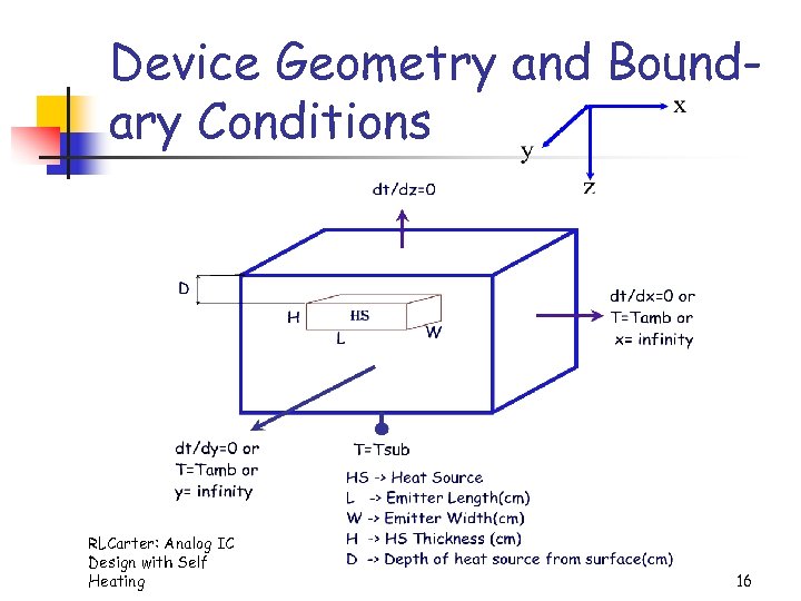 Device Geometry and Boundary Conditions RLCarter: Analog IC Design with Self Heating 16
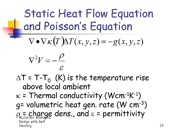 Static Heat Flow Equation and Poisson’s Equation T = T-T 0 (K) is the temperature rise above local ambient = Thermal conductivity (Wcm-1 K-1) g= volumetric heat gen. rate (W cm-3) RLCarter: Analog IC dens. , and e = permittivity = charge Design with Self Heating 17
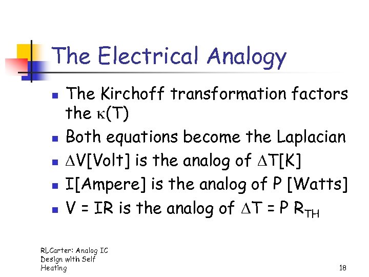 The Electrical Analogy n n n The Kirchoff transformation factors the (T) Both equations become the Laplacian V[Volt] is the analog of T[K] I[Ampere] is the analog of P [Watts] V = IR is the analog of T = P RTH RLCarter: Analog IC Design with Self Heating 18
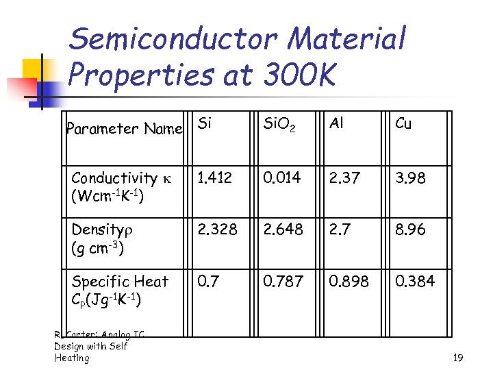 Semiconductor Material Properties at 300 K Parameter Name Si Si. O 2 Al Cu Conductivity (Wcm-1 K-1) 1. 412 0. 014 2. 37 3. 98 Density (g cm-3) 2. 328 2. 648 2. 7 8. 96 Specific Heat CP(Jg-1 K-1) 0. 787 0. 898 0. 384 RLCarter: Analog IC Design with Self Heating 19
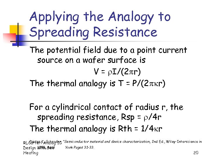 Applying the Analogy to Spreading Resistance The potential field due to a point current source on a wafer surface is V = I/(2 r) The thermal analogy is T = P/(2 r) For a cylindrical contact of radius r, the spreading resistance, Rsp = /4 r The thermal analogy is Rth = 1/4 r Dieter Analog IC RLCarter: K. Schroder, “Semiconductor material and device characterization, 2 nd Ed. , Wiley-Interscience in 1998, New York Pages 31 -33. Design with Self Heating 20
 Analog IC Design with Self-Heating Heat Source/Temperature Effects n Thermal Equations/Analogy n Thermal Resistance Models n Effect of Thermal Resistance on Device Biasing n Effect of Thermal Resistance on the Circuit Performance RLCarter: Analog IC n Conclusions/Future Work Design with Self n Heating 21
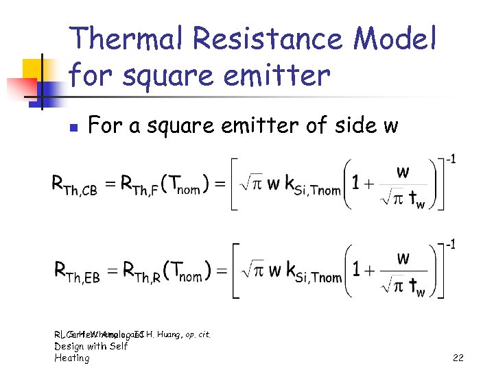 Thermal Resistance Model for square emitter n For a square emitter of side w S. H. Whemple, IC RLCarter: Analogand H. Huang, op. cit. Design with Self Heating 22
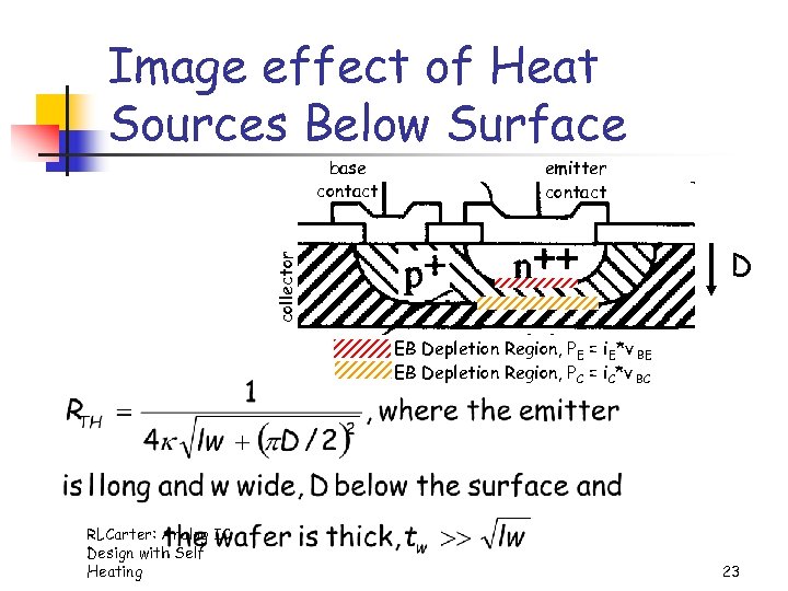 Image effect of Heat Sources Below Surface emitter contact D collector base contact EB Depletion Region, PE = i. E*v BE EB Depletion Region, PC = i. C*v BC RLCarter: Analog IC Design with Self Heating 23
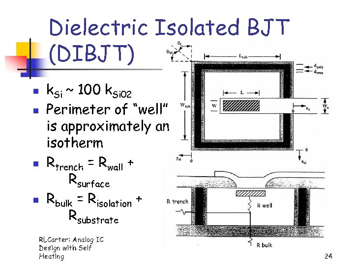 Dielectric Isolated BJT (DIBJT) n n k. Si ~ 100 k. Si 02 Perimeter of “well” is approximately an isotherm Rtrench = Rwall + Rsurface Rbulk = Risolation + Rsubstrate RLCarter: Analog IC Design with Self Heating 24
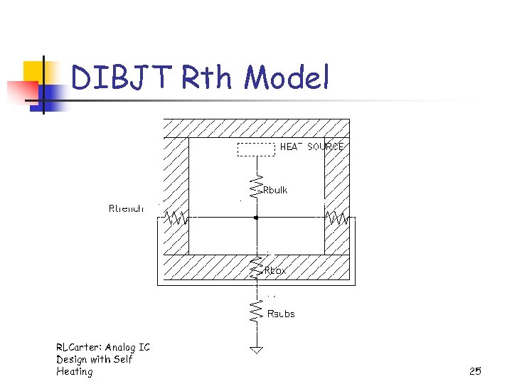 DIBJT Rth Model RLCarter: Analog IC Design with Self Heating 25
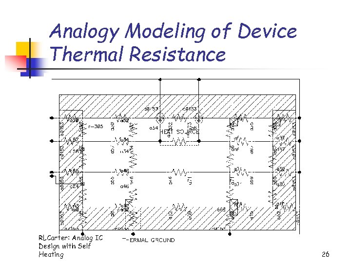 Analogy Modeling of Device Thermal Resistance RLCarter: Analog IC Design with Self Heating 26
 Analog IC Design with Self-Heating Heat Source/Temperature Effects n Thermal Equations/Analogy n Thermal Resistance Models n Effect of Thermal Resistance on Device Biasing n Effect of Thermal Resistance on the Circuit Performance RLCarter: Analog IC n Conclusions/Future Work Design with Self n Heating 27
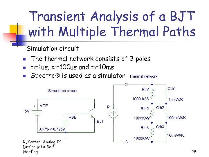 Transient Analysis of a BJT with Multiple Thermal Paths Simulation circuit n n n The thermal network consists of 3 poles 1=1 us, 2=100 us and 3=10 ms Spectre is used as a simulator RLCarter: Analog IC Design with Self Heating 28
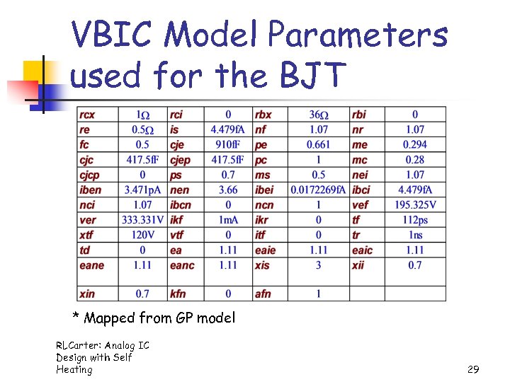 VBIC Model Parameters used for the BJT * Mapped from GP model RLCarter: Analog IC Design with Self Heating 29
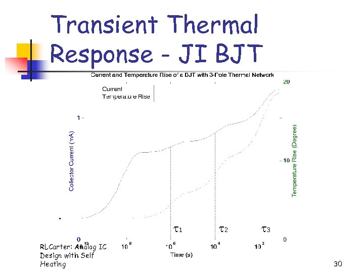 Transient Thermal Response - JI BJT 1 RLCarter: Analog IC Design with Self Heating 2 3 30
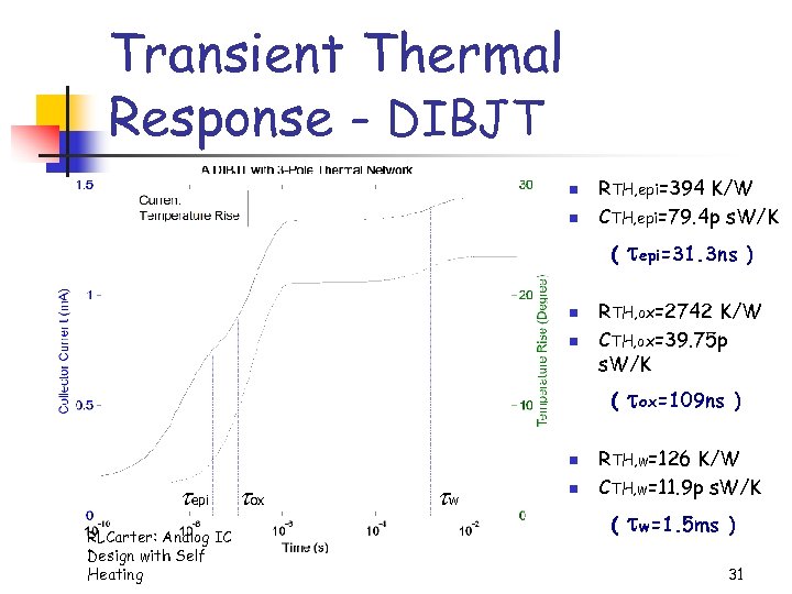 Transient Thermal Response - DIBJT n n RTH, epi=394 K/W CTH, epi=79. 4 p s. W/K ( n n epi RLCarter: Analog IC Design with Self Heating ox w n ) RTH, ox=2742 K/W CTH, ox=39. 75 p s. W/K ( n epi=31. 3 ns ox=109 ns ) RTH, w=126 K/W CTH, w=11. 9 p s. W/K ( w=1. 5 ms ) 31
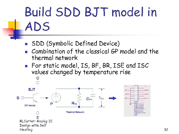 Build SDD BJT model in ADS n n n SDD (Symbolic Defined Device) Combination of the classical GP model and thermal network For static model, IS, BF, BR, ISE and ISC values changed by temperature rise RLCarter: Analog IC Design with Self Heating 32
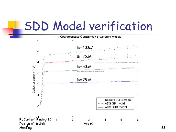 SDD Model verification IB=100 u. A IB=75 u. A IB=50 u. A IB=25 u. A RLCarter: Analog IC Design with Self Heating 33
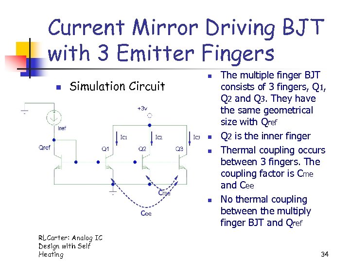 Current Mirror Driving BJT with 3 Emitter Fingers n n Simulation Circuit IC 1 IC 2 IC 3 n n cme cee RLCarter: Analog IC Design with Self Heating n The multiple finger BJT consists of 3 fingers, Q 1, Q 2 and Q 3. They have the same geometrical size with Qref Q 2 is the inner finger Thermal coupling occurs between 3 fingers. The coupling factor is Cme and Cee No thermal coupling between the multiply finger BJT and Qref 34
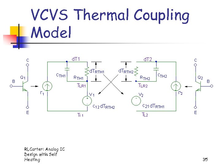 VCVS Thermal Coupling Model RLCarter: Analog IC Design with Self Heating 35
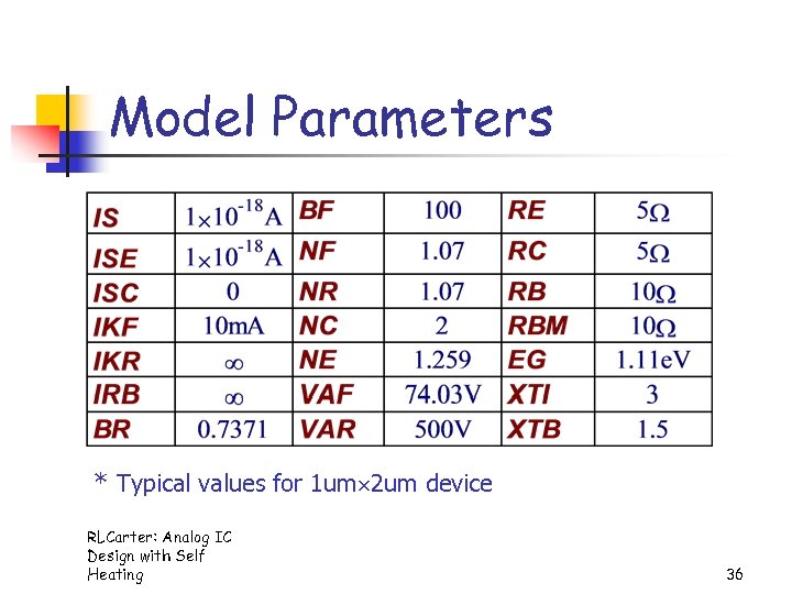 Model Parameters * Typical values for 1 um 2 um device RLCarter: Analog IC Design with Self Heating 36
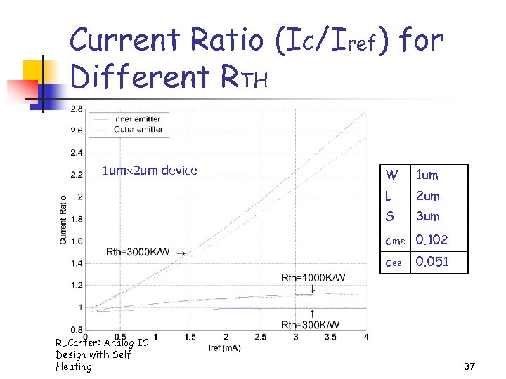 Current Ratio (IC/Iref) for Different RTH 1 um 2 um device W 1 um L 2 um S 3 um cme 0. 102 cee RLCarter: Analog IC Design with Self Heating 0. 051 37
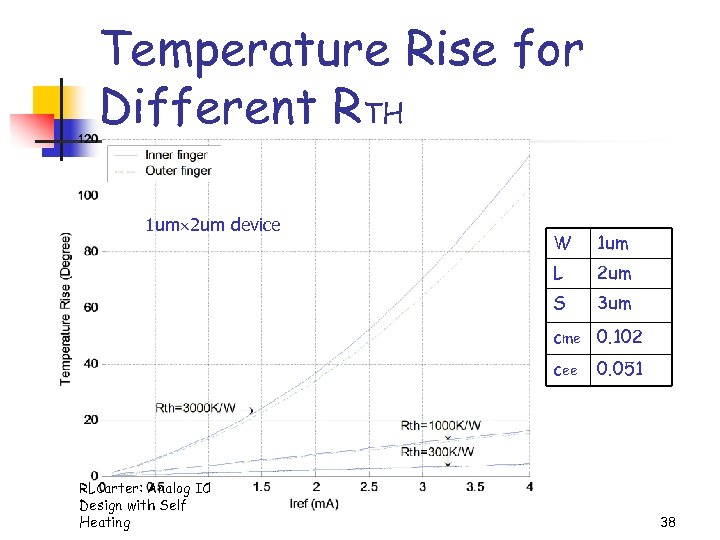 Temperature Rise for Different RTH 1 um 2 um device W 1 um L 2 um S 3 um cme 0. 102 cee RLCarter: Analog IC Design with Self Heating 0. 051 38
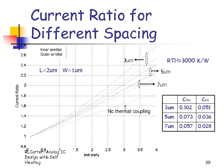 Current Ratio for Different Spacing RTH=3000 K/W 3 um L=2 um W=1 um 5 um 7 um Cme 3 um 0. 102 0. 051 5 um 0. 073 0. 036 7 um RLCarter: Analog IC Design with Self Heating Cee 0. 057 0. 028 39
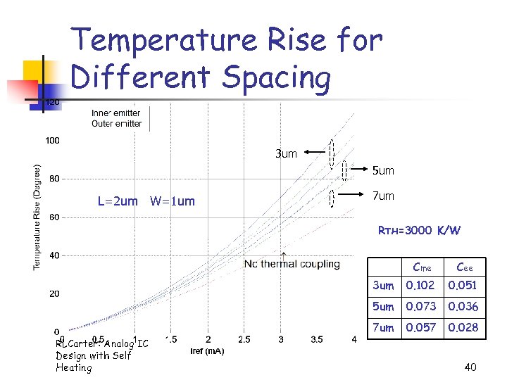 Temperature Rise for Different Spacing 3 um 5 um L=2 um W=1 um 7 um RTH=3000 K/W Cme 3 um 0. 102 0. 051 5 um 0. 073 0. 036 7 um RLCarter: Analog IC Design with Self Heating Cee 0. 057 0. 028 40
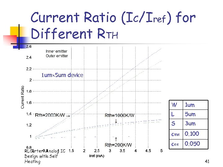 Current Ratio (IC/Iref) for Different RTH 1 um 5 um device W 1 um L 5 um S 3 um cme 0. 100 cee RLCarter: Analog IC Design with Self Heating 0. 050 41
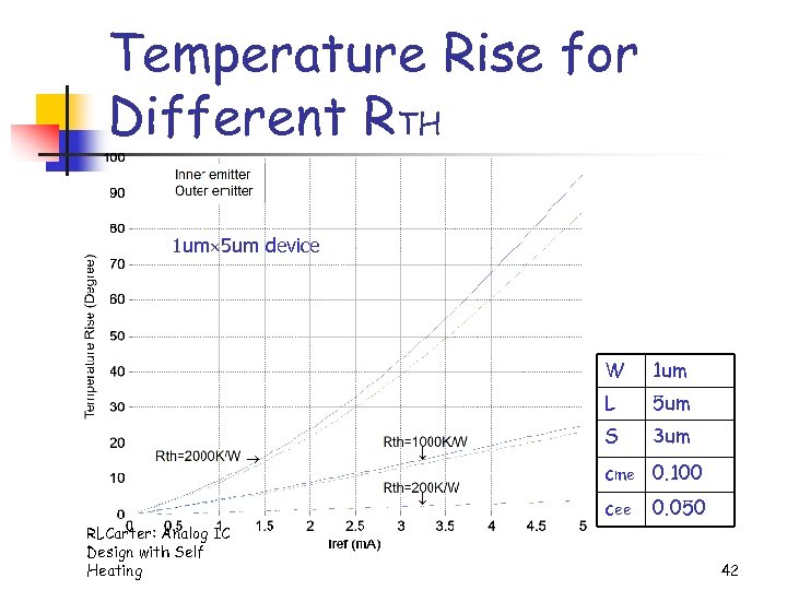 Temperature Rise for Different RTH 1 um 5 um device W 1 um L 5 um S 3 um cme 0. 100 cee RLCarter: Analog IC Design with Self Heating 0. 050 42
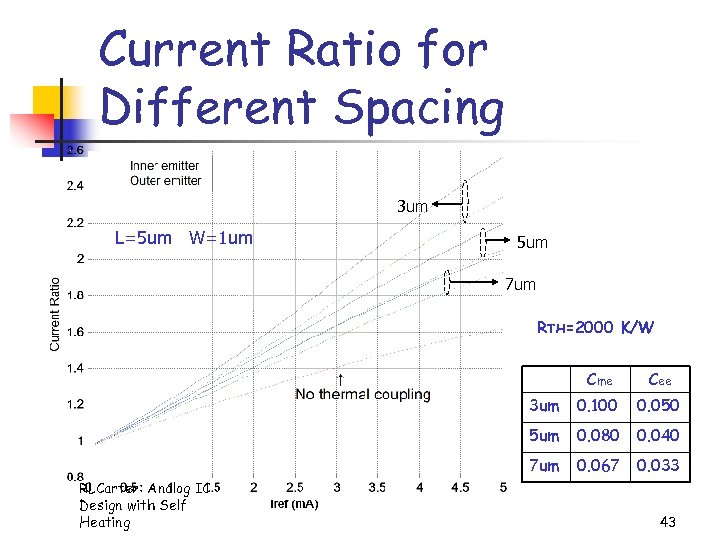 Current Ratio for Different Spacing 3 um L=5 um W=1 um 5 um 7 um RTH=2000 K/W Cme 3 um 0. 100 0. 050 5 um 0. 080 0. 040 7 um RLCarter: Analog IC Design with Self Heating Cee 0. 067 0. 033 43
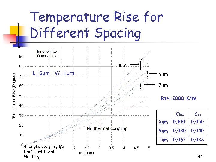 Temperature Rise for Different Spacing 3 um L=5 um W=1 um 5 um 7 um RTH=2000 K/W Cme 3 um 0. 100 0. 050 5 um 0. 080 0. 040 7 um RLCarter: Analog IC Design with Self Heating Cee 0. 067 0. 033 44
 Analog IC Design with Self-Heating Heat Source/Temperature Effects n Thermal Equations/Analogy n Thermal Resistance Models n Effect of Thermal Resistance on Device Biasing n Effect of Thermal Resistance on the Circuit Performance RLCarter: Analog IC n Conclusions/Future Work Design with Self n Heating 45
 A 741 Simulation Simulated by Spectre (Ver. 4. 4. 6. 061301) n Analog Waveform is used to obtain graphic output n Use the circuit posted on WEB (http: //wwwee. uta. edu/Online/adavis/analog/f_opamp. cir) n Transistor models are mapped to VBIC model using sgp_2_vbic (only one npn and pnp model used) n Area of Q 13 A is 0. 25; Area of Q 13 B is 0. 75 n Areas of Q 14 and Q 20 are 3 n Areas of other transistors are 1 n Connect A 741 with 15 V voltage supplies RLCarter: Analog IC n Design with Self Heating 46
![μA 741 Op-Amp Schematic RLCarter: Analog IC Design with Self Heating [1] 47 μA 741 Op-Amp Schematic RLCarter: Analog IC Design with Self Heating [1] 47](https://present5.com/presentation/b07d99a84454e628f6f15dd3b5ef7539/image-47.jpg) μA 741 Op-Amp Schematic RLCarter: Analog IC Design with Self Heating [1] 47
μA 741 Op-Amp Schematic RLCarter: Analog IC Design with Self Heating [1] 47
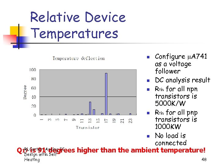 Relative Device Temperatures Configure A 741 as a voltage follower n DC analysis result n Rth for all npn transistors is 5000 K/W n Rth for all pnp transistors is 1000 KW n No load is connected RLCarter: degrees higher than the ambient temperature! Q 17 is 91 Analog IC Design with Self n Heating 48
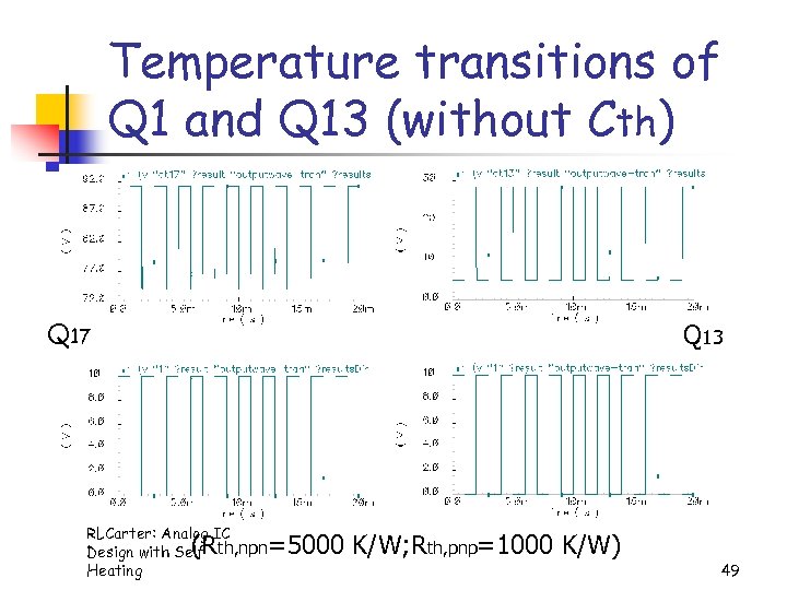 Temperature transitions of Q 1 and Q 13 (without Cth) Q 17 Q 13 RLCarter: Analog IC Design with Self th, npn Heating (R =5000 K/W; Rth, pnp=1000 K/W) 49
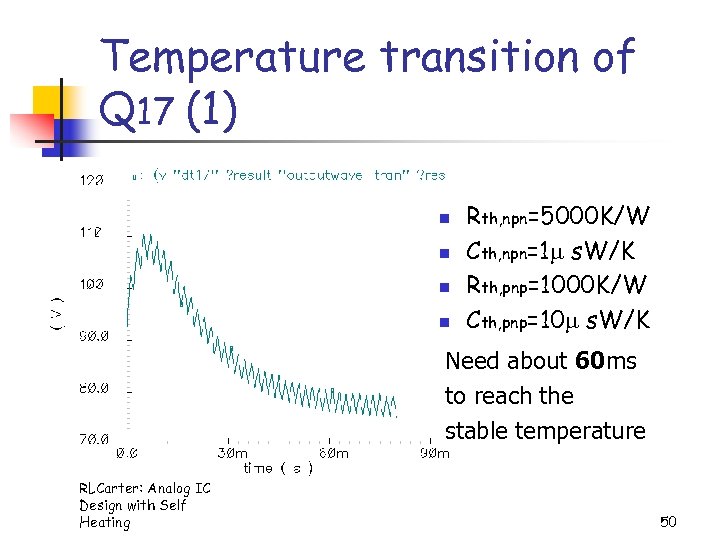 Temperature transition of Q 17 (1) n n Rth, npn=5000 K/W Cth, npn=1 s. W/K Rth, pnp=1000 K/W Cth, pnp=10 s. W/K Need about 60 ms to reach the stable temperature RLCarter: Analog IC Design with Self Heating 50
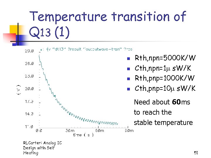 Temperature transition of Q 13 (1) n n Rth, npn=5000 K/W Cth, npn=1 s. W/K Rth, pnp=1000 K/W Cth, pnp=10 s. W/K Need about 60 ms to reach the stable temperature RLCarter: Analog IC Design with Self Heating 51
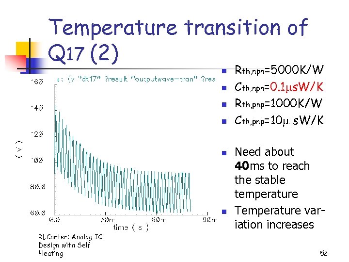 Temperature transition of Q 17 (2) n n n RLCarter: Analog IC Design with Self Heating Rth, npn=5000 K/W Cth, npn=0. 1 s. W/K Rth, pnp=1000 K/W Cth, pnp=10 s. W/K Need about 40 ms to reach the stable temperature Temperature variation increases 52
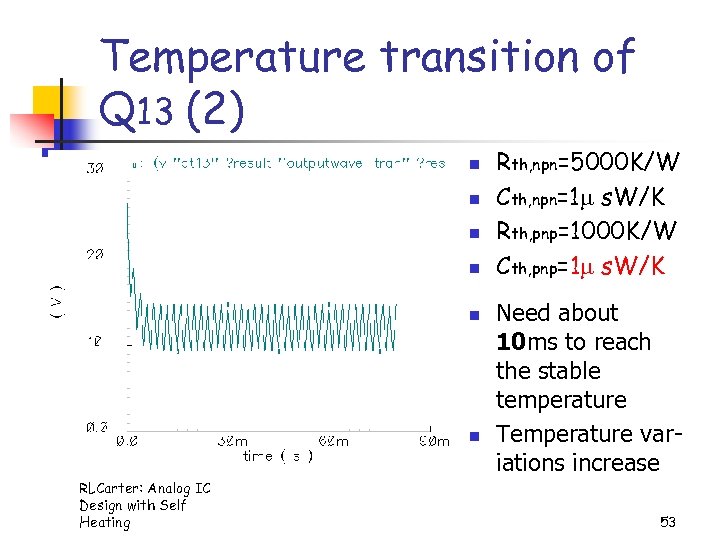 Temperature transition of Q 13 (2) n n n RLCarter: Analog IC Design with Self Heating Rth, npn=5000 K/W Cth, npn=1 s. W/K Rth, pnp=1000 K/W Cth, pnp=1 s. W/K Need about 10 ms to reach the stable temperature Temperature variations increase 53
![Circuit used to measure the open loop gain[2] Simulation parameters: n n n Use Circuit used to measure the open loop gain[2] Simulation parameters: n n n Use](https://present5.com/presentation/b07d99a84454e628f6f15dd3b5ef7539/image-54.jpg) Circuit used to measure the open loop gain[2] Simulation parameters: n n n Use a feedback technique to determine the open loop gain DUT is the op amp to be tested Nulling op amp is connected in a feedback mode RLCarter: Analog IC Design with Self Heating n n n R 1=100 R 2=1 M R 3=1 K Vmid=0 VSRC 1 sweeps from 0 to 1 V 54
Circuit used to measure the open loop gain[2] Simulation parameters: n n n Use a feedback technique to determine the open loop gain DUT is the op amp to be tested Nulling op amp is connected in a feedback mode RLCarter: Analog IC Design with Self Heating n n n R 1=100 R 2=1 M R 3=1 K Vmid=0 VSRC 1 sweeps from 0 to 1 V 54
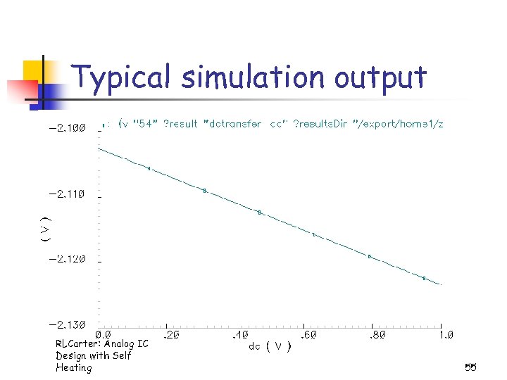 Typical simulation output RLCarter: Analog IC Design with Self Heating 55
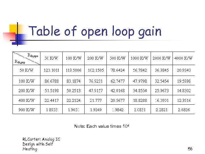 Table of open loop gain Note: Each value times 104 RLCarter: Analog IC Design with Self Heating 56
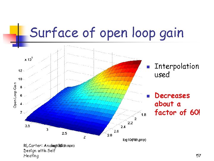 Surface of open loop gain n n RLCarter: Analog IC Design with Self Heating Interpolation used Decreases about a factor of 60! 57
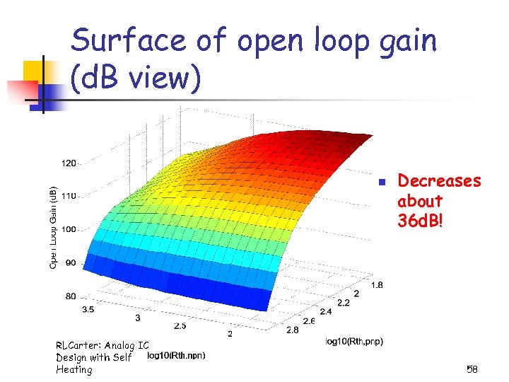 Surface of open loop gain (d. B view) n RLCarter: Analog IC Design with Self Heating Decreases about 36 d. B! 58
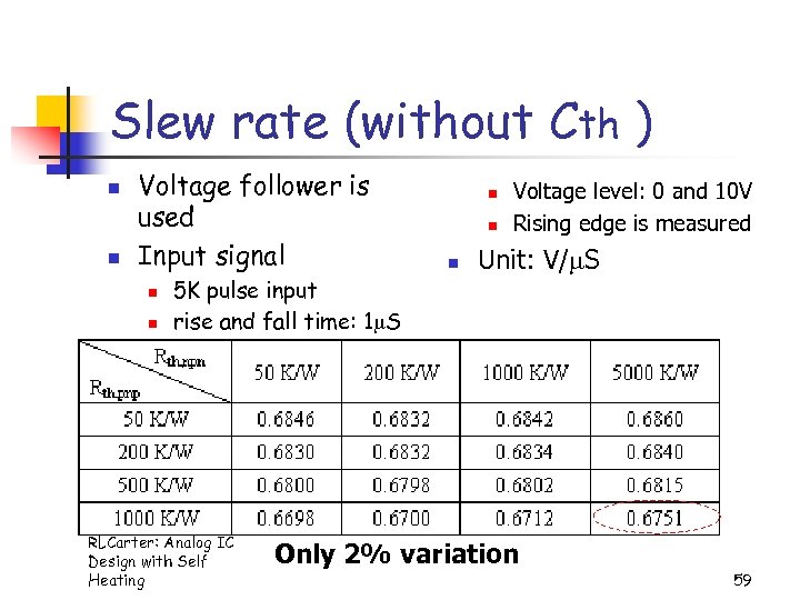 Slew rate (without Cth ) n n Voltage follower is used Input signal n n 5 K pulse input rise and fall time: 1 S RLCarter: Analog IC Design with Self Heating n n n Voltage level: 0 and 10 V Rising edge is measured Unit: V/ S Only 2% variation 59
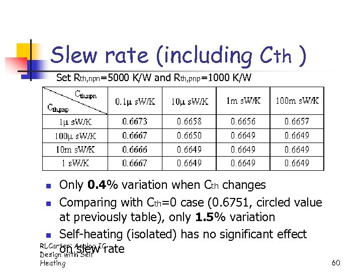 Slew rate (including Cth ) Set Rth, npn=5000 K/W and Rth, pnp=1000 K/W Only 0. 4% variation when Cth changes n Comparing with Cth=0 case (0. 6751, circled value at previously table), only 1. 5% variation n Self-heating (isolated) has no significant effect RLCarter: Analog IC on slew rate Design with Self n Heating 60
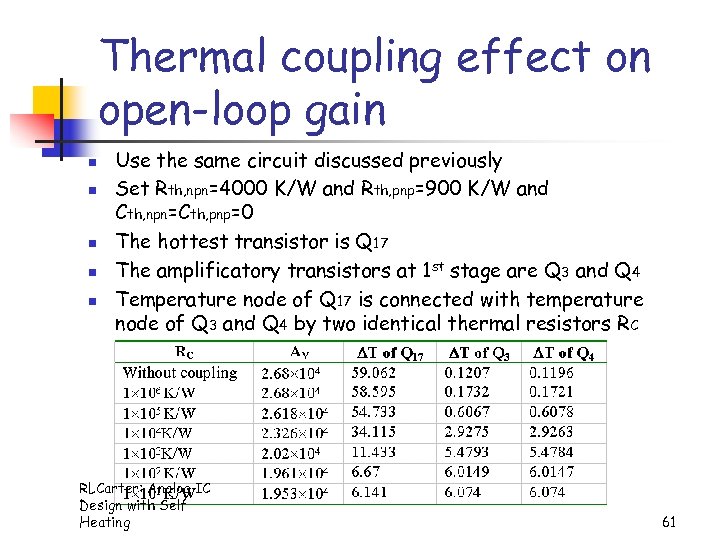 Thermal coupling effect on open-loop gain n n Use the same circuit discussed previously Set Rth, npn=4000 K/W and Rth, pnp=900 K/W and Cth, npn=Cth, pnp=0 The hottest transistor is Q 17 The amplificatory transistors at 1 st stage are Q 3 and Q 4 Temperature node of Q 17 is connected with temperature node of Q 3 and Q 4 by two identical thermal resistors RC RLCarter: Analog IC Design with Self Heating 61
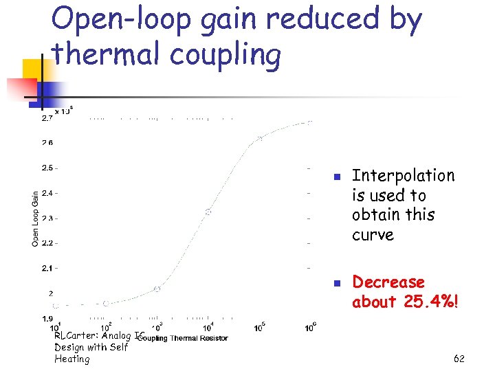 Open-loop gain reduced by thermal coupling n n RLCarter: Analog IC Design with Self Heating Interpolation is used to obtain this curve Decrease about 25. 4%! 62
 Analog IC Design with Self-Heating Heat Source/Temperature Effects n Thermal Equations/Analogy n Thermal Resistance Models n Effect of Thermal Resistance on Device Biasing n Effect of Thermal Resistance on the Circuit Performance RLCarter: Analog IC n Conclusions/Future Work Design with Self n Heating 63
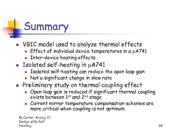 Summary n VBIC model used to analyze thermal effects n n n Isolated self-heating in A 741 n n n Effect of individual device temperatures in a A 741 Inter-device heating effects Isolated self-heating can reduce the open loop gain Not a significant change in slew rate Preliminary study on thermal coupling effect n n Open loop gain is reduced if significant thermal coupling exists between 1 st and 2 nd stage Current mirror temperature compensation schemes are more critical when coupling is not optimum. RLCarter: Analog IC Design with Self Heating 64
 Acknowledgements: Support n n n The. Texas Higher Education Coordinating Board (THECB) National Semiconductor Corporation (NSC) The National Science Foundation Industry/University Center for Electronic Materials, Devices and Systems (NSF/CEMDAS) RLCarter: Analog IC Design with Self Heating 65
 Acknowledgements: Analog IC Research Group n n n n Professor W. Alan Davis Zhipeng Zhu Zheng Li Siddharth Nashiney Naveen Kumar Reddy Siddareddygari Shankaranarayanan Rajaraman Piyush Thacker Anurag Lakhlani RLCarter: Analog IC Design with Self Heating 66
 References Paul R. Gray, Robert G. Meyer, et al, Analysis and design of analog integrated circuits, New York: Wiley, c 2001 Fujiang Lin, et al, “Extraction Of VBIC Model for Si. Ge HBTs Made Easy by Going Through Gummel-Poon Model”, from http: //eesof. tm. agilent. com/pdf/VBIC_Model_Extraction. pdf http: //www. fht-esslingen. de/institute/iafgp/neu/VBIC/ Avanti Star-spice User Manual, 04, 2001. Affirma Spectre Circuit Simulator Device Model Equations Zweidinger, D. T. ; Fox, R. M. , et al, “Equivalent circuit modeling of static substrate thermal coupling using VCVS representation”, Solid-State Circuits, IEEE Journal of , Volume: 2 Issue: 9 , Sept. 2002, Page(s): 1198 -1206 Jonathan S. Brodsky, “Physics based impedance models for the simulation of self-heating in semiconductor devices and circuits”, Ph. D Dissertation, Dept of Electrical and Computer Engineering, University of Florida, Gainesville, Aug 1997. Mc. Andrew, C. , Seitchik, J. and etal, ” VBIC 95: An improved vertical, IC bipolar transistor model”, Bipolar/Bi. CMOS Circuits and Technology Meeting, 1995. , Proceedings of the 1995 Burns and Robert, An introduction to mixed-signal testing, Oxford University Press, 1999 Copyright Texas Instruments RLCarter: Analog IC Design with Self Heating 67


