2033aa01050151be811b3cf6f37abcfa.ppt
- Количество слайдов: 148
 High Density isp. LSI Families © LATTICE SEMICONDUCTOR CORPORATION 2000 Uudet mikropiirit High Density January 2008 1 Lattice Confidential
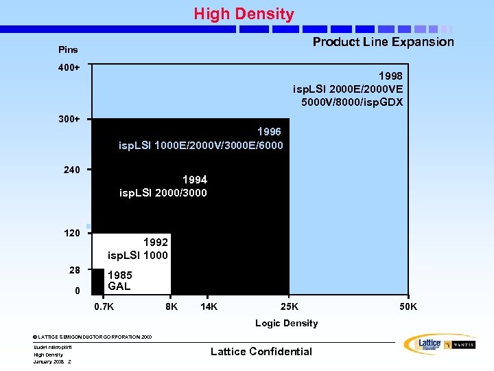 High Density Product Line Expansion Pins 400+ 1998 isp. LSI 2000 E/2000 VE 5000 V/8000/isp. GDX 300+ 1996 isp. LSI 1000 E/2000 V/3000 E/6000 240 120 28 0 1994 isp. LSI 2000/3000 1992 isp. LSI 1000 1985 GAL 0. 7 K 8 K 14 K 25 K Logic Density © LATTICE SEMICONDUCTOR CORPORATION 2000 Uudet mikropiirit High Density January 2008 2 Lattice Confidential 50 K
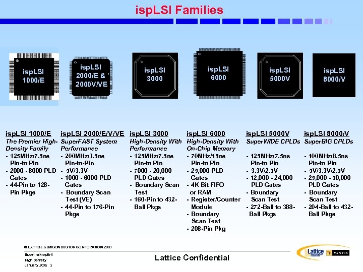 isp. LSI Families isp. LSI 1000/E isp. LSI 2000/E & 2000 V/VE isp. LSI 3000 isp. LSI 6000 isp. LSI 5000 V isp. LSI 8000/V isp. LSI 1000/E isp. LSI 2000/E/V/VE isp. LSI 3000 isp. LSI 6000 isp. LSI 5000 V The Premier High. Density Family - 125 MHz/7. 5 ns Pin-to Pin - 2000 - 8000 PLD Gates - 44 -Pin to 128 Pin Pkgs Super. FAST System Performance - 200 MHz/3. 5 ns Pin-to-Pin - 5 V/3. 3 V - 1000 - 6000 PLD Gates - Boundary Scan Test (VE) - 44 -Pin to 176 -Pin Pkgs High-Density With On-Chip Memory - 70 MHz/15 ns Pin-to Pin - 25, 000 PLD Gates - 4 K Bit FIFO or RAM - Register/Counter Module - Boundary Scan Test - 208 -Pin Pkg Super. WIDE CPLDs Super. BIG CPLDs High-Density With Performance - 125 MHz/7. 5 ns Pin-to Pin - 7000 - 20, 000 PLD Gates - Boundary Scan Test - 160 -Pin to 432 Ball Pkgs © LATTICE SEMICONDUCTOR CORPORATION 2000 Uudet mikropiirit High Density January 2008 3 Lattice Confidential - 125 MHz/7. 5 ns Pin-to Pin - 3. 3 V/2. 5 V - 12, 000 - 24, 000 PLD Gates - Boundary Scan Test - 272 -Ball to 388 Ball Pkgs isp. LSI 8000/V - 100 MHz/8. 5 ns Pin-to Pin - 5 V/3. 3 V/2. 5 V - 25, 000 - 50, 000 PLD Gates - Boundary Scan Test - 204 -Ball to 432 Ball Pkgs
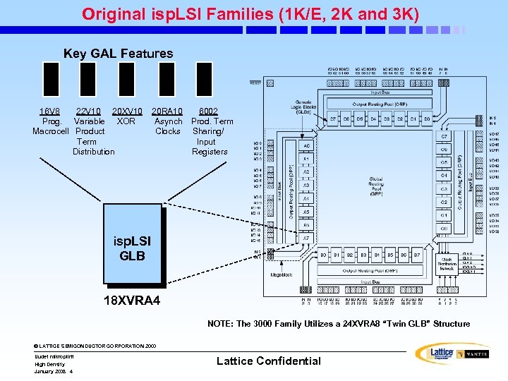 Original isp. LSI Families (1 K/E, 2 K and 3 K) Key GAL Features 16 V 8 22 V 10 20 XV 10 Prog. Variable XOR Macrocell Product Term Distribution 20 RA 10 Asynch Clocks 6002 Prod. Term Sharing/ Input Registers isp. LSI GLB 18 XVRA 4 NOTE: The 3000 Family Utilizes a 24 XVRA 8 “Twin GLB” Structure © LATTICE SEMICONDUCTOR CORPORATION 2000 Uudet mikropiirit High Density January 2008 4 Lattice Confidential
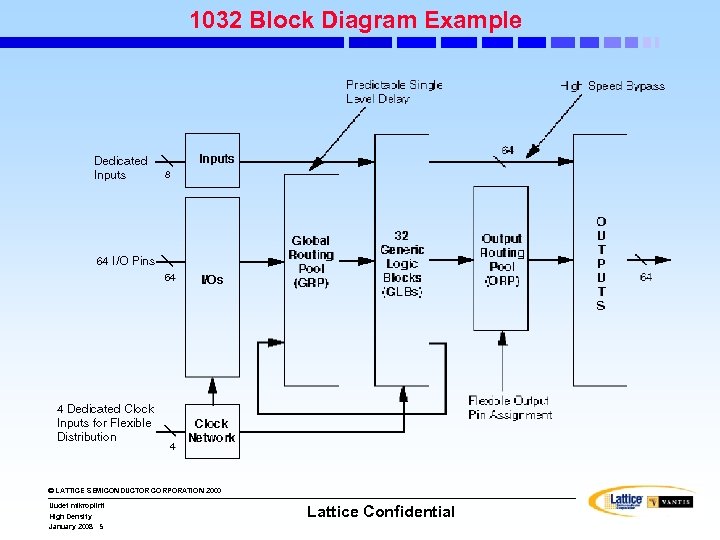 1032 Block Diagram Example © LATTICE SEMICONDUCTOR CORPORATION 2000 Uudet mikropiirit High Density January 2008 5 Lattice Confidential
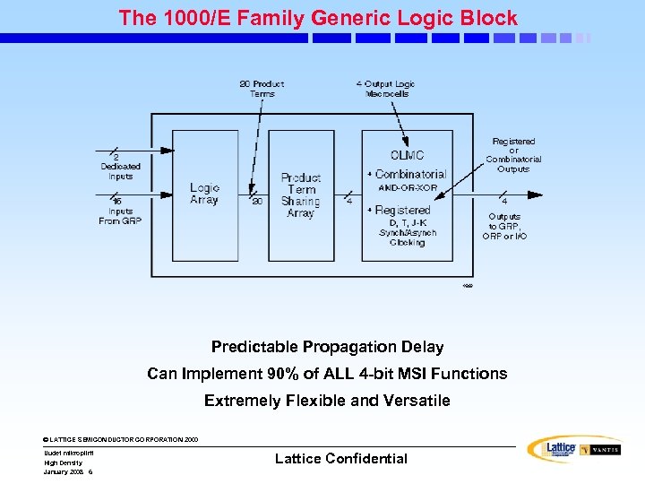 The 1000/E Family Generic Logic Block Predictable Propagation Delay Can Implement 90% of ALL 4 -bit MSI Functions Extremely Flexible and Versatile © LATTICE SEMICONDUCTOR CORPORATION 2000 Uudet mikropiirit High Density January 2008 6 Lattice Confidential
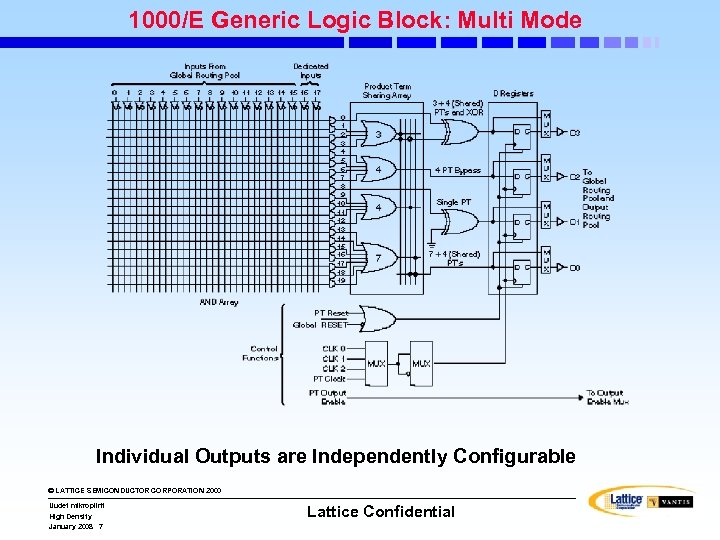 1000/E Generic Logic Block: Multi Mode Individual Outputs are Independently Configurable © LATTICE SEMICONDUCTOR CORPORATION 2000 Uudet mikropiirit High Density January 2008 7 Lattice Confidential
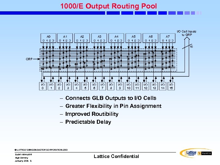 1000/E Output Routing Pool – – Connects GLB Outputs to I/O Cells Greater Flexibility in Pin Assignment Improved Routibility Predictable Delay © LATTICE SEMICONDUCTOR CORPORATION 2000 Uudet mikropiirit High Density January 2008 8 Lattice Confidential
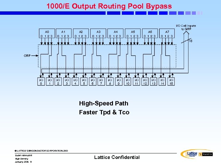 1000/E Output Routing Pool Bypass High-Speed Path Faster Tpd & Tco © LATTICE SEMICONDUCTOR CORPORATION 2000 Uudet mikropiirit High Density January 2008 9 Lattice Confidential
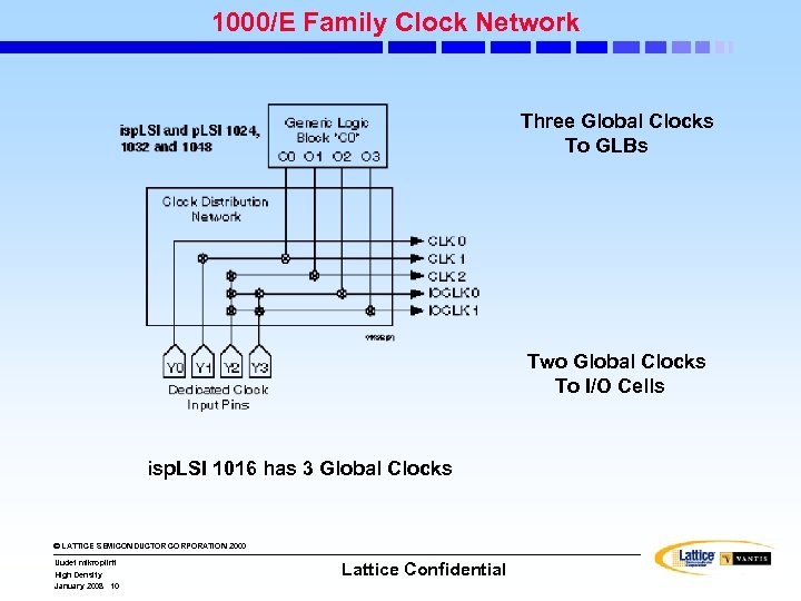 1000/E Family Clock Network Three Global Clocks To GLBs Two Global Clocks To I/O Cells isp. LSI 1016 has 3 Global Clocks © LATTICE SEMICONDUCTOR CORPORATION 2000 Uudet mikropiirit High Density January 2008 10 Lattice Confidential
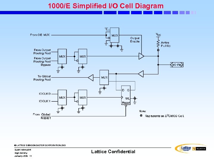 1000/E Simplified I/O Cell Diagram © LATTICE SEMICONDUCTOR CORPORATION 2000 Uudet mikropiirit High Density January 2008 11 Lattice Confidential
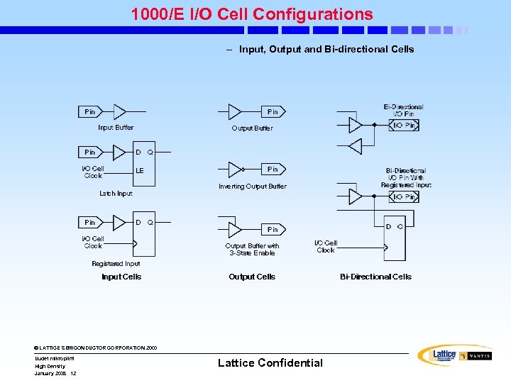 1000/E I/O Cell Configurations – Input, Output and Bi-directional Cells © LATTICE SEMICONDUCTOR CORPORATION 2000 Uudet mikropiirit High Density January 2008 12 Lattice Confidential
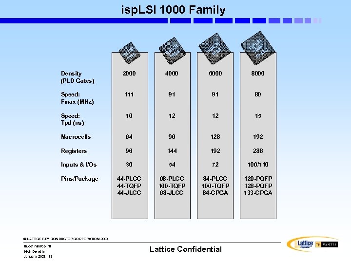 isp. LSI 1000 Family I LS sp 16 i 0 1 I LS sp 24 i 0 1 I LS sp 32 i 0 1 I LS sp 48/ i 10 48 C 10 Density (PLD Gates) 2000 4000 6000 8000 Speed: Fmax (MHz) 111 91 91 80 Speed: Tpd (ns) 10 12 12 15 Macrocells 64 96 128 192 Registers 96 144 192 288 Inputs & I/Os 36 54 72 106/110 Pins/Package 44 -PLCC 44 -TQFP 44 -JLCC 68 -PLCC 100 -TQFP 68 -JLCC 84 -PLCC 100 -TQFP 84 -CPGA 120 -PQFP 128 -PQFP 133 -CPGA © LATTICE SEMICONDUCTOR CORPORATION 2000 Uudet mikropiirit High Density January 2008 13 Lattice Confidential
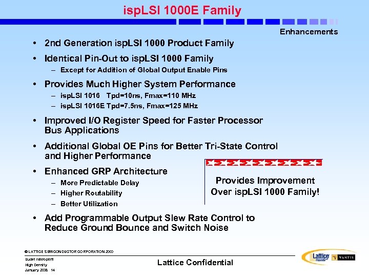 isp. LSI 1000 E Family Enhancements • 2 nd Generation isp. LSI 1000 Product Family • Identical Pin-Out to isp. LSI 1000 Family – Except for Addition of Global Output Enable Pins • Provides Much Higher System Performance – isp. LSI 1016 Tpd=10 ns, Fmax=110 MHz – isp. LSI 1016 E Tpd=7. 5 ns, Fmax=125 MHz • Improved I/O Register Speed for Faster Processor Bus Applications • Additional Global OE Pins for Better Tri-State Control and Higher Performance • Enhanced GRP Architecture – More Predictable Delay – Higher Routability – Better Utilization Provides Improvement Over isp. LSI 1000 Family! • Add Programmable Output Slew Rate Control to Reduce Ground Bounce and Switch Noise © LATTICE SEMICONDUCTOR CORPORATION 2000 Uudet mikropiirit High Density January 2008 14 Lattice Confidential
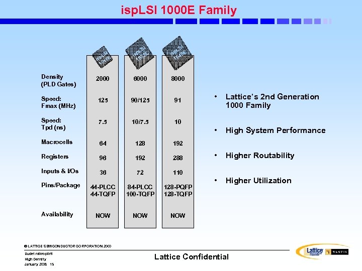 isp. LSI 1000 E Family SI p. L 6 E is 1 10 SI p. L 2 E is 3 10 I LS isp 48 E 10 Density (PLD Gates) 2000 6000 8000 Speed: Fmax (MHz) 125 90/125 91 Speed: Tpd (ns) 7. 5 10/7. 5 10 Macrocells 64 128 192 Registers 96 192 288 Inputs & I/Os 36 72 110 Pins/Package 44 -PLCC 44 -TQFP 84 -PLCC 100 -TQFP 128 -PQFP 128 -TQFP NOW NOW Availability • Lattice’s 2 nd Generation 1000 Family • High System Performance • Higher Routability • Higher Utilization © LATTICE SEMICONDUCTOR CORPORATION 2000 Uudet mikropiirit High Density January 2008 15 Lattice Confidential
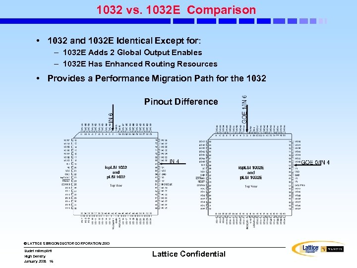 1032 vs. 1032 E Comparison • 1032 and 1032 E Identical Except for: – 1032 E Adds 2 Global Output Enables – 1032 E Has Enhanced Routing Resources • Provides a Performance Migration Path for the 1032 Pinout Difference © LATTICE SEMICONDUCTOR CORPORATION 2000 Uudet mikropiirit High Density January 2008 16 Lattice Confidential
 isp. LSI 2000 Family © LATTICE SEMICONDUCTOR CORPORATION 2000 Uudet mikropiirit High Density January 2008 17 Lattice Confidential
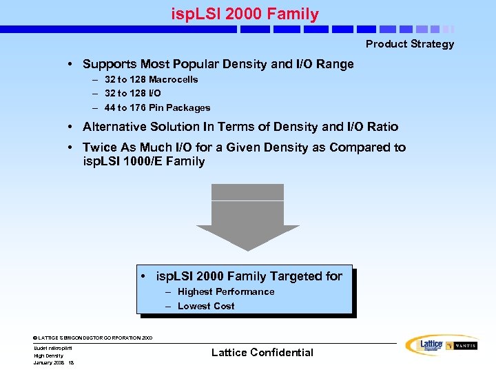 isp. LSI 2000 Family Product Strategy • Supports Most Popular Density and I/O Range – 32 to 128 Macrocells – 32 to 128 I/O – 44 to 176 Pin Packages • Alternative Solution In Terms of Density and I/O Ratio • Twice As Much I/O for a Given Density as Compared to isp. LSI 1000/E Family • isp. LSI 2000 Family Targeted for – Highest Performance – Lowest Cost © LATTICE SEMICONDUCTOR CORPORATION 2000 Uudet mikropiirit High Density January 2008 18 Lattice Confidential
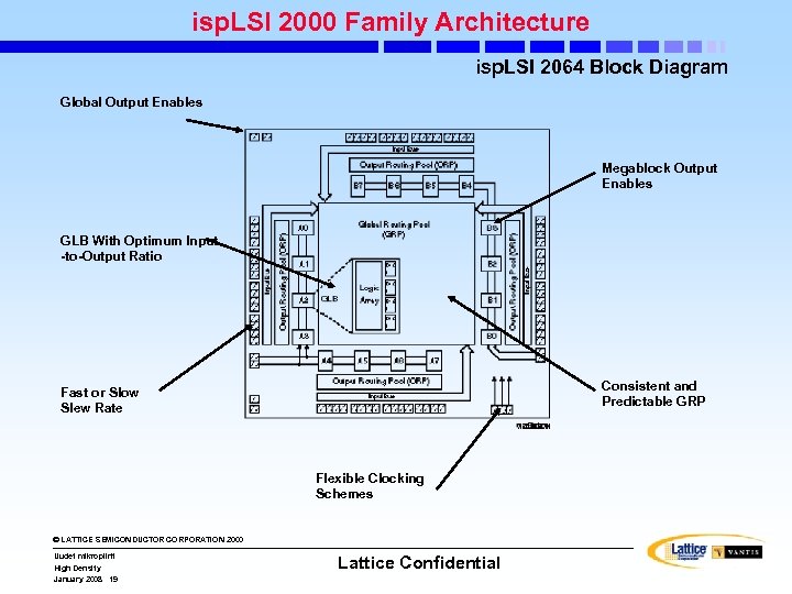 isp. LSI 2000 Family Architecture isp. LSI 2064 Block Diagram Global Output Enables Megablock Output Enables GLB With Optimum Input -to-Output Ratio Consistent and Predictable GRP Fast or Slow Slew Rate Flexible Clocking Schemes © LATTICE SEMICONDUCTOR CORPORATION 2000 Uudet mikropiirit High Density January 2008 19 Lattice Confidential
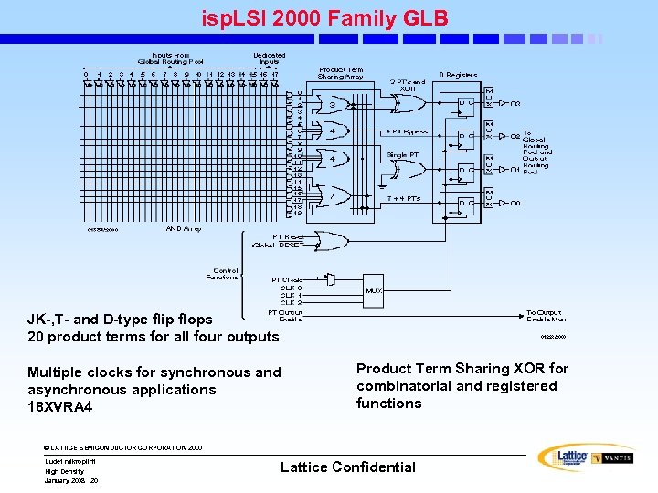 isp. LSI 2000 Family GLB JK-, T- and D-type flip flops 20 product terms for all four outputs Multiple clocks for synchronous and asynchronous applications 18 XVRA 4 Product Term Sharing XOR for combinatorial and registered functions © LATTICE SEMICONDUCTOR CORPORATION 2000 Uudet mikropiirit High Density January 2008 20 Lattice Confidential
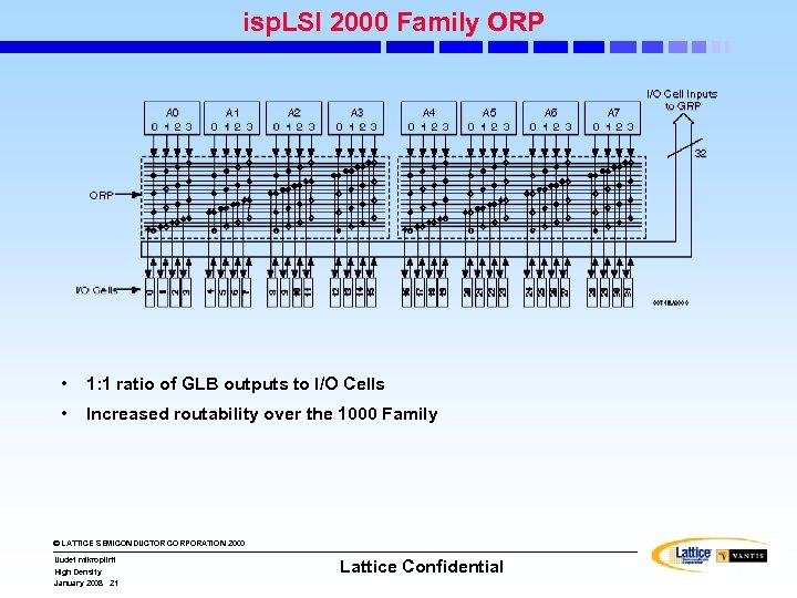 isp. LSI 2000 Family ORP • 1: 1 ratio of GLB outputs to I/O Cells • Increased routability over the 1000 Family © LATTICE SEMICONDUCTOR CORPORATION 2000 Uudet mikropiirit High Density January 2008 21 Lattice Confidential
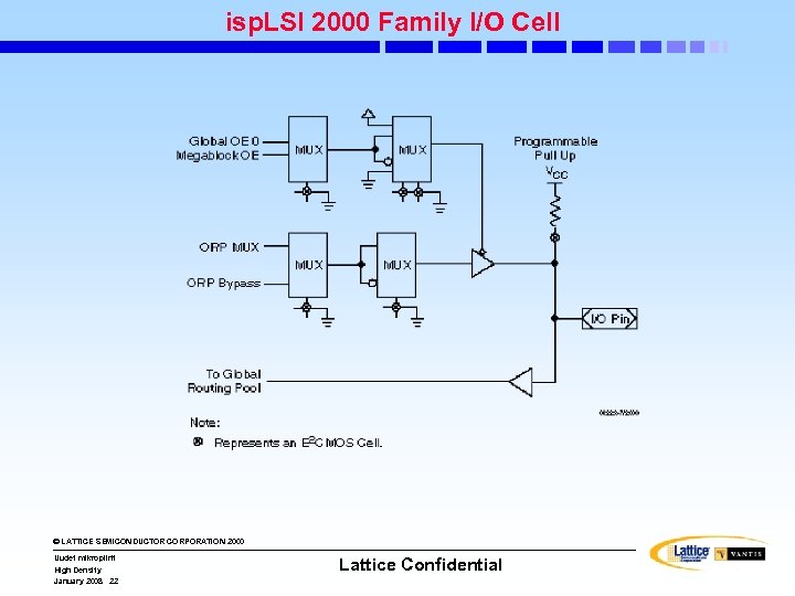 isp. LSI 2000 Family I/O Cell © LATTICE SEMICONDUCTOR CORPORATION 2000 Uudet mikropiirit High Density January 2008 22 Lattice Confidential
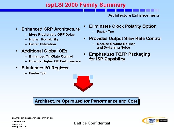 isp. LSI 2000 Family Summary Architecture Enhancements • Enhanced GRP Architecture – More Predictable GRP Delay – Higher Routability – Better Utilization • Additional Global OEs – Enhanced Tri-State Control – Provide Higher OE Performance • Eliminates Clock Polarity Option – Faster Tco • Provides Output Slew Rate Control – Reduce Ground Bounce and Switching Noise • Emphasizes TQFP Packaging for ISP Capability • Eliminates I/O Register – Faster Tpd Architecture Optimized for Performance and Cost © LATTICE SEMICONDUCTOR CORPORATION 2000 Uudet mikropiirit High Density January 2008 23 Lattice Confidential
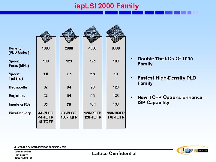 isp. LSI 2000 Family I LS isp 032 2 SI p. L 4 is 06 2 I LS sp 96 i 0 2 SI p. L 8 is 12 2 Density (PLD Gates) 1000 2000 4000 6000 Speed: Fmax (MHz) 180 125 100 Speed: Tpd (ns) 5. 0 7. 5 10 Macrocells 32 64 96 128 Registers 32 64 96 128 Inputs & I/Os 35 70 104 138 Pins/Package 44 -PLCC 44 -TQFP 48 -TQFP 84 -PLCC 100 -TQFP 128 -PQFP 128 -TQFP 160 -MQFP 176 -TQFP • Double The I/Os Of 1000 Family • Fastest High-Density PLD Family • New TQFP Options Enhance ISP Capability © LATTICE SEMICONDUCTOR CORPORATION 2000 Uudet mikropiirit High Density January 2008 24 Lattice Confidential
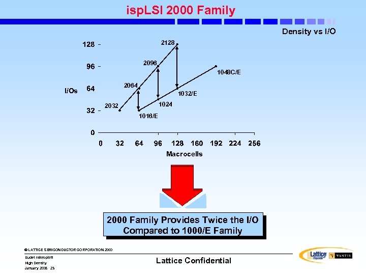 isp. LSI 2000 Family Density vs I/O 2128 2096 1048 C/E 2064 I/Os 1032/E 1024 2032 1016/E Macrocells 2000 Family Provides Twice the I/O Compared to 1000/E Family © LATTICE SEMICONDUCTOR CORPORATION 2000 Uudet mikropiirit High Density January 2008 25 Lattice Confidential
 isp. LSI 2000 E Family © LATTICE SEMICONDUCTOR CORPORATION 2000 Uudet mikropiirit High Density January 2008 26 Lattice Confidential
 isp. LSI 2000 V Family © LATTICE SEMICONDUCTOR CORPORATION 2000 Uudet mikropiirit High Density January 2008 27 Lattice Confidential
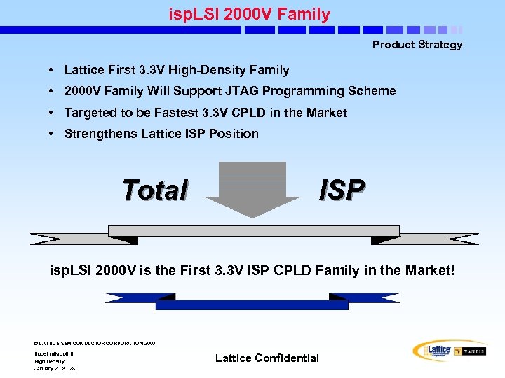 isp. LSI 2000 V Family Product Strategy • Lattice First 3. 3 V High-Density Family • 2000 V Family Will Support JTAG Programming Scheme • Targeted to be Fastest 3. 3 V CPLD in the Market • Strengthens Lattice ISP Position Total ISP isp. LSI 2000 V is the First 3. 3 V ISP CPLD Family in the Market! © LATTICE SEMICONDUCTOR CORPORATION 2000 Uudet mikropiirit High Density January 2008 28 Lattice Confidential
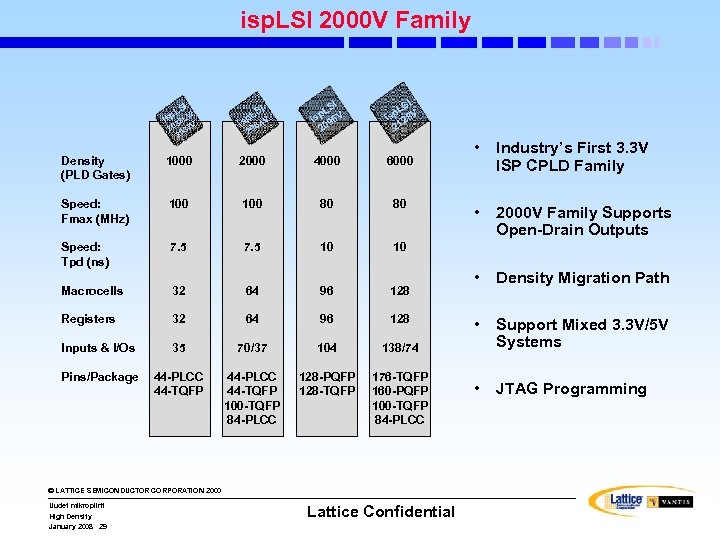 isp. LSI 2000 V Family I LS / isp 2 LV 3 20 032 V 2 is 64 0 2 SI p. L 6 V is 9 20 I LS sp 28 V i 21 SI p. L V Density (PLD Gates) 1000 2000 4000 6000 Speed: Fmax (MHz) 100 80 80 Speed: Tpd (ns) 7. 5 10 32 64 96 128 Registers 32 64 96 128 Inputs & I/Os 35 70/37 104 44 -PLCC 44 -TQFP 100 -TQFP 84 -PLCC 128 -PQFP 128 -TQFP 176 -TQFP 160 -PQFP 100 -TQFP 84 -PLCC • 2000 V Family Supports Open-Drain Outputs • Density Migration Path • Support Mixed 3. 3 V/5 V Systems • JTAG Programming 138/74 Pins/Package Industry’s First 3. 3 V ISP CPLD Family 10 Macrocells • © LATTICE SEMICONDUCTOR CORPORATION 2000 Uudet mikropiirit High Density January 2008 29 Lattice Confidential
 isp. LSI 3000 Family © LATTICE SEMICONDUCTOR CORPORATION 2000 Uudet mikropiirit High Density January 2008 30 Lattice Confidential
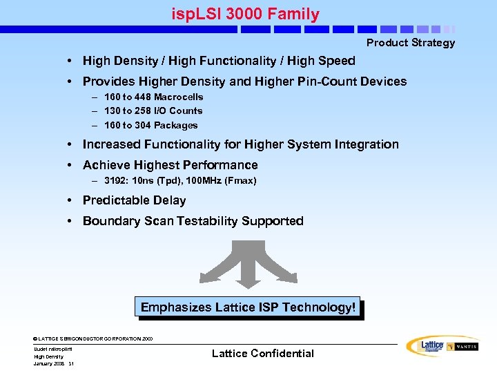 isp. LSI 3000 Family Product Strategy • High Density / High Functionality / High Speed • Provides Higher Density and Higher Pin-Count Devices – 160 to 448 Macrocells – 130 to 258 I/O Counts – 160 to 304 Packages • Increased Functionality for Higher System Integration • Achieve Highest Performance – 3192: 10 ns (Tpd), 100 MHz (Fmax) • Predictable Delay • Boundary Scan Testability Supported Emphasizes Lattice ISP Technology! © LATTICE SEMICONDUCTOR CORPORATION 2000 Uudet mikropiirit High Density January 2008 31 Lattice Confidential
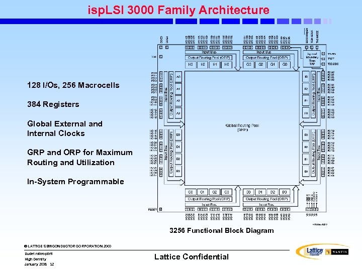 isp. LSI 3000 Family Architecture 128 I/Os, 256 Macrocells 384 Registers Global External and Internal Clocks GRP and ORP for Maximum Routing and Utilization In-System Programmable 3256 Functional Block Diagram © LATTICE SEMICONDUCTOR CORPORATION 2000 Uudet mikropiirit High Density January 2008 32 Lattice Confidential
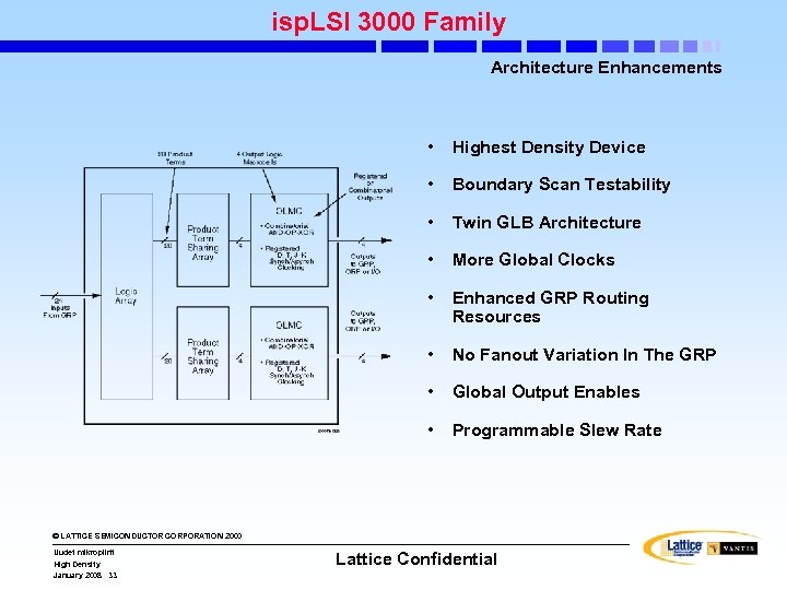 isp. LSI 3000 Family Architecture Enhancements • Highest Density Device • Boundary Scan Testability • Twin GLB Architecture • More Global Clocks • Enhanced GRP Routing Resources • No Fanout Variation In The GRP • Global Output Enables • Programmable Slew Rate © LATTICE SEMICONDUCTOR CORPORATION 2000 Uudet mikropiirit High Density January 2008 33 Lattice Confidential
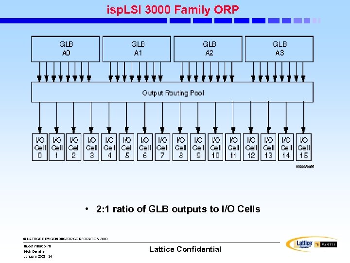 isp. LSI 3000 Family ORP • 2: 1 ratio of GLB outputs to I/O Cells © LATTICE SEMICONDUCTOR CORPORATION 2000 Uudet mikropiirit High Density January 2008 34 Lattice Confidential
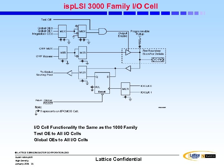 isp. LSI 3000 Family I/O Cell Functionality the Same as the 1000 Family Test OE to All I/O Cells Global OEs to All I/O Cells © LATTICE SEMICONDUCTOR CORPORATION 2000 Uudet mikropiirit High Density January 2008 35 Lattice Confidential
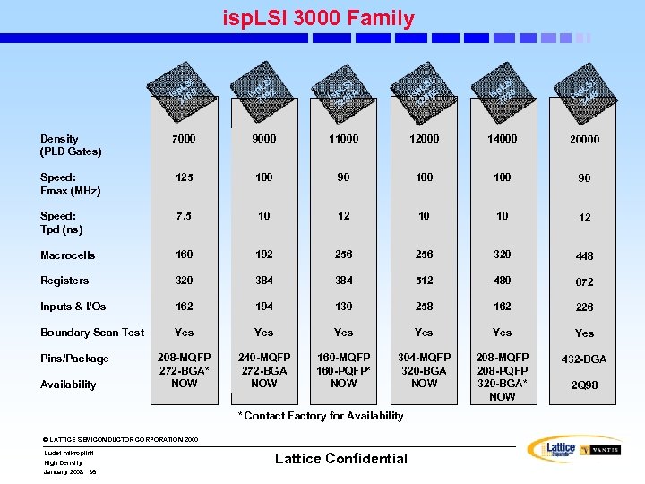 isp. LSI 3000 Family SI p. L 0 is 16 3 I LS sp 92 i 1 3 SI p. L 6 A is 5 32 SI p. L 6 E is 5 32 I LS sp 20 i 3 3 SI p. L 8 is 44 3 Density (PLD Gates) 7000 9000 11000 12000 14000 20000 Speed: Fmax (MHz) 125 100 90 Speed: Tpd (ns) 7. 5 10 12 10 10 12 Macrocells 160 192 256 320 448 Registers 320 384 512 480 672 Inputs & I/Os 162 194 130 258 162 226 Boundary Scan Test Yes Yes Yes 208 -MQFP 272 -BGA* NOW 240 -MQFP 272 -BGA NOW 160 -MQFP 160 -PQFP* NOW 304 -MQFP 320 -BGA NOW 208 -MQFP 208 -PQFP 320 -BGA* NOW 432 -BGA Pins/Package Availability * Contact Factory for Availability © LATTICE SEMICONDUCTOR CORPORATION 2000 Uudet mikropiirit High Density January 2008 36 Lattice Confidential 2 Q 98
 Introduction to Vantis Programmable Logic Devices MACH 1 and MACH 2 CPLD Families MACH 5 Family MACH 4 Family JTAG ISP © LATTICE SEMICONDUCTOR CORPORATION 2000 Uudet mikropiirit High Density January 2008 46 Lattice Confidential
 Agenda • Vantis value propositions • Vantis MACH 1 CPLD Family • Vantis MACH 2 CPLD Family • Vantis MACH 5 CPLD Family architecture • Vantis MACH 4 CPLD Family architecture • Compare and Contrast • JTAG ISP © LATTICE SEMICONDUCTOR CORPORATION 2000 Uudet mikropiirit High Density January 2008 47 Lattice Confidential
 Vantis Value Propositions • Speed. Locked performance • Ease-of-Use • Multiple Density - I/O combinations • Reliability • Advanced system integration features © LATTICE SEMICONDUCTOR CORPORATION 2000 Uudet mikropiirit High Density January 2008 48 Lattice Confidential
 Mach 1 and 2 © LATTICE SEMICONDUCTOR CORPORATION 2000 Uudet mikropiirit High Density January 2008 49 Lattice Confidential
 MACH 1 & MACH 2 Architectures Principal performance features of the MACH 1 & MACH 2 Architectures are: • Central switch matrix • Product-Term (PT) arrays -- programmable “AND” planes • Logic Allocators -- fixed “OR” planes • Multimode macrocells • PAL Block OE (Output Enable) Product-Terms © LATTICE SEMICONDUCTOR CORPORATION 2000 Uudet mikropiirit High Density January 2008 50 Lattice Confidential
 MACH 1 & MACH 2 Features and Characteristics • Original MACH Architectures • Highly Routable • Power Management Feature – Per Macrocell and Per Block power-down • Guaranteed Speed. Locked Timing – up to 12 PT for M 1 – up to 16 PT for M 2 • Multiple Density and I/O Combinations • Commercial and Industrial Devices Available • Up to sixteen Product-Term functions are accommodated © LATTICE SEMICONDUCTOR CORPORATION 2000 Uudet mikropiirit High Density January 2008 51 Lattice Confidential
 MACH 1 & MACH 2 Performance: Speeds and Densities • Speed Performance – Commercial as fast as t. PD = 5 ns (FCNT = 182 MHz) – Industrial as fast as t. PD = 7. 5 ns • Mid-Range Densities – 32 to 128 macrocells – 32 to 64 I/Os – 4 to 16 output enable controls © LATTICE SEMICONDUCTOR CORPORATION 2000 Uudet mikropiirit High Density January 2008 52 Lattice Confidential
 MACH 1 & MACH 2 Performance: System Capabilities • Devices are In-System Programmable (‘SP’ devices only) • Devices are JTAG (IEEE 1149. 1) compatible (‘SP’ devices only) – Do not have a boundary-scan register so test is not possible • PCI-compliant (Speed Grades 7 ns, 10 ns and 12 ns • Device I/Os are “Bus-Friendly” • Devices have a programmable security bit • Devices follow a pre-set power-up procedure • Power Management Feature -- Full or Half-Power © LATTICE SEMICONDUCTOR CORPORATION 2000 Uudet mikropiirit High Density January 2008 53 Lattice Confidential
 MACH 1 & MACH 2 Performance: Technology & Support • Leading-edge process technology – The EE 6. 5 process – L(EFF) = 0. 5 micron • Supported by Design. Direct and IDE software • Low-cost entry-level tool • Windows GUI interface © LATTICE SEMICONDUCTOR CORPORATION 2000 Uudet mikropiirit High Density January 2008 54 Lattice Confidential
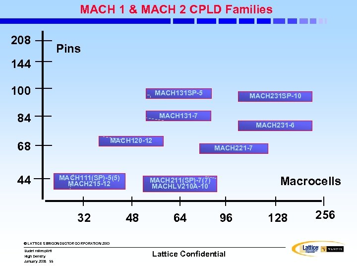 MACH 1 & MACH 2 CPLD Families 208 Pins 144 100 MACH 131 SP-5 84 MACH 131 -7 MACH 231 -6 MACH 120 -12 68 44 MACH 231 SP-10 MACH 111(SP)-5(5) MACH 215 -12 32 MACH 221 -7 Macrocells MACH 211(SP)-7(7) MACHLV 210 A-10 48 64 96 © LATTICE SEMICONDUCTOR CORPORATION 2000 Uudet mikropiirit High Density January 2008 55 Lattice Confidential 128 256
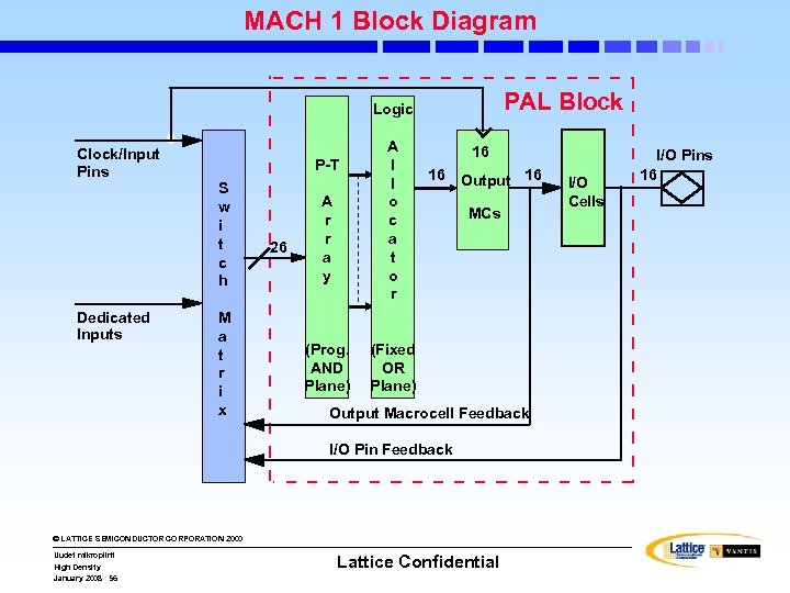 MACH 1 Block Diagram PAL Block Logic Clock/Input Pins Dedicated Inputs P-T S w i t c h M a t r i x 26 A r r a y (Prog. AND Plane) A l l o c a t o r 16 16 Output 16 MCs (Fixed OR Plane) Output Macrocell Feedback I/O Pin Feedback © LATTICE SEMICONDUCTOR CORPORATION 2000 Uudet mikropiirit High Density January 2008 56 Lattice Confidential I/O Cells I/O Pins 16
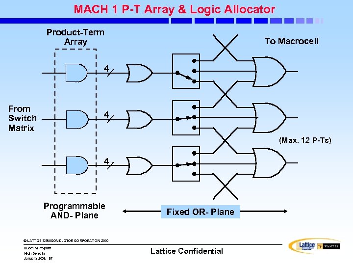 MACH 1 P-T Array & Logic Allocator Product-Term Array To Macrocell 4 From Switch Matrix 4 (Max. 12 P-Ts) 4 Programmable AND- Plane Fixed OR- Plane © LATTICE SEMICONDUCTOR CORPORATION 2000 Uudet mikropiirit High Density January 2008 57 Lattice Confidential
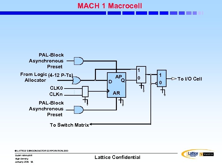 MACH 1 Macrocell PAL-Block Asynchronous Preset From Logic (4 -12 P-Ts) Allocator CLK 0 CLKn 1 AP Q D 0 AR PAL-Block Asynchronous Preset To Switch Matrix © LATTICE SEMICONDUCTOR CORPORATION 2000 Uudet mikropiirit High Density January 2008 58 Lattice Confidential 1 0 To I/O Cell
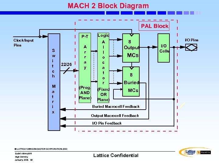 MACH 2 Block Diagram PAL Block Logic P-T Clock/Input Pins S w i t c h 22/26 M a t r i x A l l o c a t o r A r r a y (Prog. AND Plane) (Fixed OR Plane) 8 Output MCs 8 Buried MCs Buried Macrocell Feedback Output Macrocell Feedback I/O Pin Feedback © LATTICE SEMICONDUCTOR CORPORATION 2000 Uudet mikropiirit High Density January 2008 59 Lattice Confidential I/O Pins I/O Cells
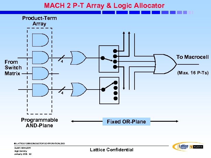 MACH 2 P-T Array & Logic Allocator Product-Term Array From Switch Matrix To Macrocell 4 (Max. 16 P-Ts) 4 Programmable AND-Plane Fixed OR-Plane © LATTICE SEMICONDUCTOR CORPORATION 2000 Uudet mikropiirit High Density January 2008 60 Lattice Confidential
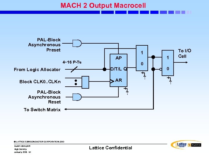 MACH 2 Output Macrocell PAL-Block Asynchronous Preset 1 4~16 P-Ts From Logic Allocator Block CLK 0. . CLKn AP 0 D/T/L Q AR PAL-Block Asynchronous Reset To Switch Matrix © LATTICE SEMICONDUCTOR CORPORATION 2000 Uudet mikropiirit High Density January 2008 61 Lattice Confidential 1 0 To I/O Cell
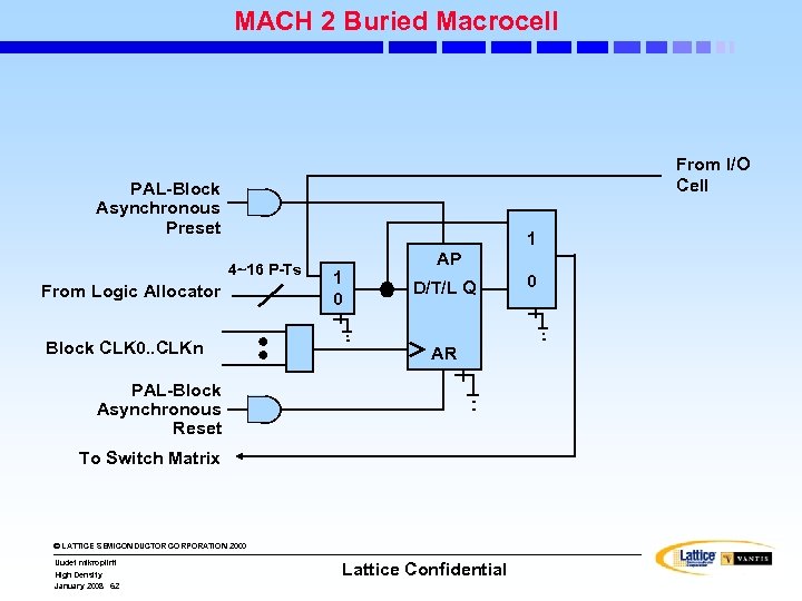 MACH 2 Buried Macrocell From I/O Cell PAL-Block Asynchronous Preset 1 4~16 P-Ts From Logic Allocator Block CLK 0. . CLKn 1 0 AP D/T/L Q AR PAL-Block Asynchronous Reset To Switch Matrix © LATTICE SEMICONDUCTOR CORPORATION 2000 Uudet mikropiirit High Density January 2008 62 Lattice Confidential 0
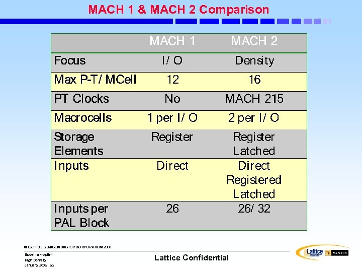 MACH 1 & MACH 2 Comparison © LATTICE SEMICONDUCTOR CORPORATION 2000 Uudet mikropiirit High Density January 2008 63 Lattice Confidential
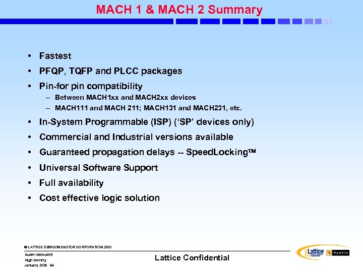 MACH 1 & MACH 2 Summary • Fastest • PFQP, TQFP and PLCC packages • Pin-for pin compatibility – Between MACH 1 xx and MACH 2 xx devices – MACH 111 and MACH 211; MACH 131 and MACH 231, etc. • In-System Programmable (ISP) (‘SP’ devices only) • Commercial and Industrial versions available • Guaranteed propagation delays -- Speed. Locking • Universal Software Support • Full availability • Cost effective logic solution © LATTICE SEMICONDUCTOR CORPORATION 2000 Uudet mikropiirit High Density January 2008 64 Lattice Confidential
 Mach 5 © LATTICE SEMICONDUCTOR CORPORATION 2000 Uudet mikropiirit High Density January 2008 65 Lattice Confidential
 MACH 5(A) CPLD Family Overview • MACH 5(A) Family Performance Characteristics • MACH 5(A) Architecture – MACH 5(A) Internal “Components” and Subsystems • MACH 5(A) Timing and Delay © LATTICE SEMICONDUCTOR CORPORATION 2000 Uudet mikropiirit High Density January 2008 66 Lattice Confidential
 MACH 5(A) Performance Characteristics • Fifth Generation MACH Architecture • Hierarchical signal routability • Both 5 V and 3. 3 V versions • Up to 32 Product-Terms per macrocell, with true XOR capability © LATTICE SEMICONDUCTOR CORPORATION 2000 Uudet mikropiirit High Density January 2008 67 Lattice Confidential
 MACH 5(A) Performance Characteristics (cont’d) • Power Management Feature – Four PAL block-based power versus speed options • Synchronous and Asynchronous clocking – Single- & Dual-edge clocking • Fixed, predictable delays © LATTICE SEMICONDUCTOR CORPORATION 2000 Uudet mikropiirit High Density January 2008 68 Lattice Confidential
 Performance: Speed and Densities • High Densities – 128 to 512 macrocells – 16 to 64 output enable controls • Speed Performance – Commercial t. PD = 5. 5 ns (f. CNT = 182 MHz) – Industrial t. PD = 7. 5 ns • Nine packages offered – Accommodate from 68 to 256 signal I/Os • Multiple package/density options © LATTICE SEMICONDUCTOR CORPORATION 2000 Uudet mikropiirit High Density January 2008 69 Lattice Confidential
 Performance: System Capabilities • 5 V and 3. 3 V JEDEC-compliant • In-System programmable • JTAG (IEEE 1149. 1) compliant • PCI-compliant (Speed Grades -5, -7, -10 and -12) • M 5 A devices can be hot-socketed © LATTICE SEMICONDUCTOR CORPORATION 2000 Uudet mikropiirit High Density January 2008 70 Lattice Confidential
 Performance: System Capabilities (cont’d) • Mixed supply voltage system-safe • I/Os are “Bus-Friendly” – M 5 A I/Os have programmable pull-up option • Individual device I/Os are slew-rate controllable • Devices have a programmable security bit • Power Management capability – Block-by-block basis – Four levels of power reduction © LATTICE SEMICONDUCTOR CORPORATION 2000 Uudet mikropiirit High Density January 2008 71 Lattice Confidential
 Performance: Technology and Support • Leading-edge process technologies: – EE 8 process -- 0. 25 micron (Leff), 3. 3 V » All M 5 A devices – EE 7 process -- 0. 35 micron (Leff), 3. 3 V » M 5 -320, M 5 -384, M 5 -512 » All M 5 LV (3. 3 v) devices – The EE 6. 5 process -- 0. 5 micron (Leff) » M 5 -128, M 5 -192 and M 5 -256 © LATTICE SEMICONDUCTOR CORPORATION 2000 Uudet mikropiirit High Density January 2008 72 Lattice Confidential
 Performance: Technology and Support • Supported by Design. Direct software – Low-cost entry-level tool with Design. Direct » Windows GUI interface » OEM Package with synthesis and simulation • Supported by Vantis MACHXL software – Design entry ports to universal tools • Supported by isp. Design. Expert software © LATTICE SEMICONDUCTOR CORPORATION 2000 Uudet mikropiirit High Density January 2008 73 Lattice Confidential
 Performance: MACH 5(A) Advancements • Greater density range • More I/O and Density points • More packages • Higher speed • More clocking options • Lower power dissipation • Lower cost © LATTICE SEMICONDUCTOR CORPORATION 2000 Uudet mikropiirit High Density January 2008 74 Lattice Confidential
 MACH 5(A) Architecture • MACH 5(A) Principal Performance Features: • Three levels of interconnect • Product-Term arrays • Logic Allocators • Multimode Macrocells • Control (Clock, Set and Reset) Generators • OE (Output Enable) Generators © LATTICE SEMICONDUCTOR CORPORATION 2000 Uudet mikropiirit High Density January 2008 75 Lattice Confidential
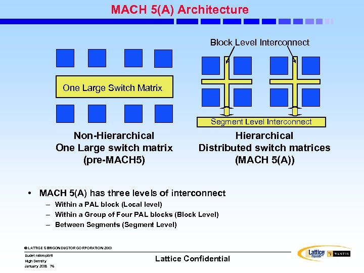 MACH 5(A) Architecture Block Level Interconnect One Large Switch Matrix Segment Level Interconnect Non-Hierarchical One Large switch matrix (pre-MACH 5) Hierarchical Distributed switch matrices (MACH 5(A)) • MACH 5(A) has three levels of interconnect – Within a PAL block (Local level) – Within a Group of Four PAL blocks (Block Level) – Between Segments (Segment Level) © LATTICE SEMICONDUCTOR CORPORATION 2000 Uudet mikropiirit High Density January 2008 76 Lattice Confidential
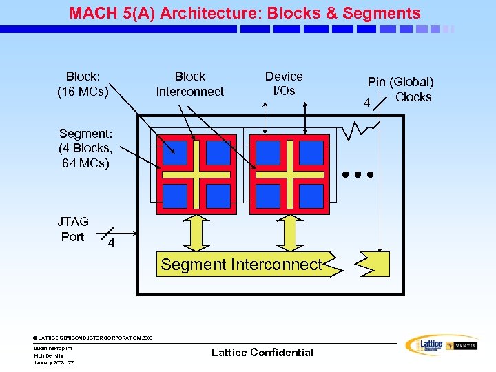 MACH 5(A) Architecture: Blocks & Segments Block: (16 MCs) Block Interconnect Device I/Os Segment: (4 Blocks, 64 MCs) JTAG Port 4 Segment Interconnect © LATTICE SEMICONDUCTOR CORPORATION 2000 Uudet mikropiirit High Density January 2008 77 Lattice Confidential Pin (Global) Clocks 4
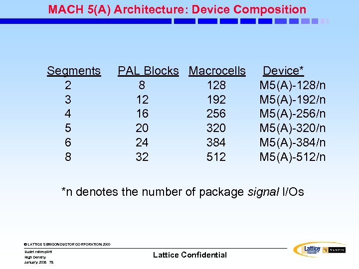 MACH 5(A) Architecture: Device Composition Segments 2 3 4 5 6 8 PAL Blocks Macrocells 8 12 192 16 256 20 320 24 384 32 512 Device* M 5(A)-128/n M 5(A)-192/n M 5(A)-256/n M 5(A)-320/n M 5(A)-384/n M 5(A)-512/n *n denotes the number of package signal I/Os © LATTICE SEMICONDUCTOR CORPORATION 2000 Uudet mikropiirit High Density January 2008 78 Lattice Confidential
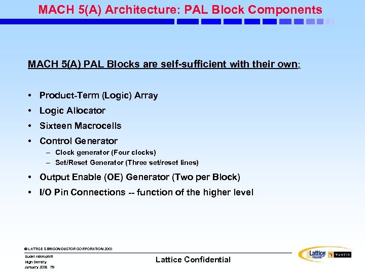 MACH 5(A) Architecture: PAL Block Components MACH 5(A) PAL Blocks are self-sufficient with their own: • Product-Term (Logic) Array • Logic Allocator • Sixteen Macrocells • Control Generator – Clock generator (Four clocks) – Set/Reset Generator (Three set/reset lines) • Output Enable (OE) Generator (Two per Block) • I/O Pin Connections -- function of the higher level © LATTICE SEMICONDUCTOR CORPORATION 2000 Uudet mikropiirit High Density January 2008 79 Lattice Confidential
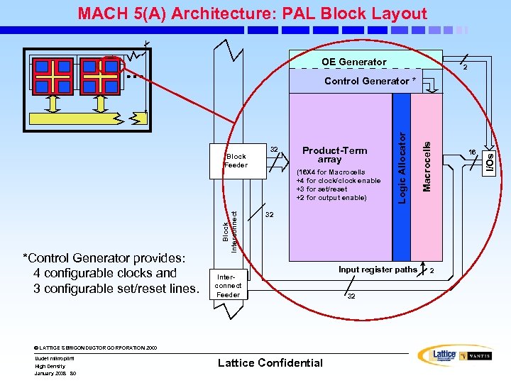 MACH 5(A) Architecture: PAL Block Layout OE Generator 2 *Control Generator provides: 4 configurable clocks and 3 configurable set/reset lines. Block Interconnect Product-Term array (16 X 4 for Macrocells +4 for clock/clock enable +3 for set/reset +2 for output enable) 32 Interconnect Feeder © LATTICE SEMICONDUCTOR CORPORATION 2000 Uudet mikropiirit High Density January 2008 80 Lattice Confidential Input register paths 32 2 16 I/Os 32 Macrocells Block Feeder Logic Allocator Control Generator *
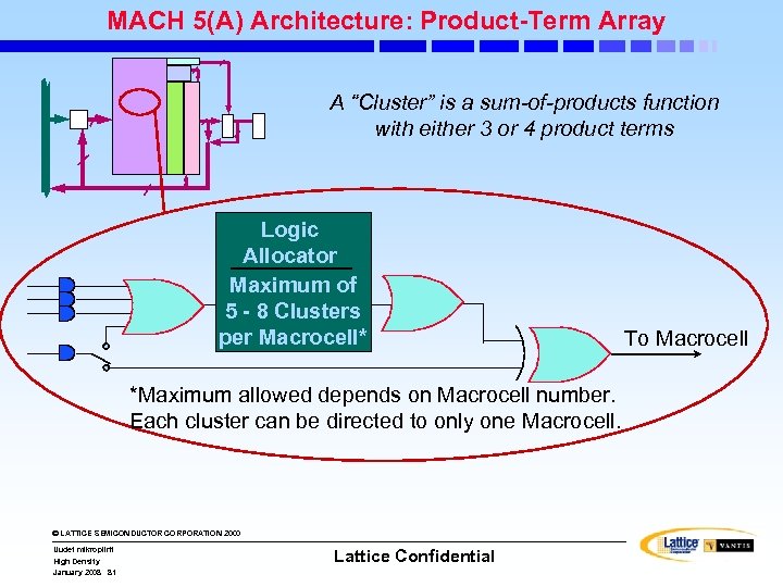 MACH 5(A) Architecture: Product-Term Array A “Cluster” is a sum-of-products function with either 3 or 4 product terms Logic Allocator Maximum of 5 - 8 Clusters per Macrocell* *Maximum allowed depends on Macrocell number. Each cluster can be directed to only one Macrocell. © LATTICE SEMICONDUCTOR CORPORATION 2000 Uudet mikropiirit High Density January 2008 81 Lattice Confidential To Macrocell
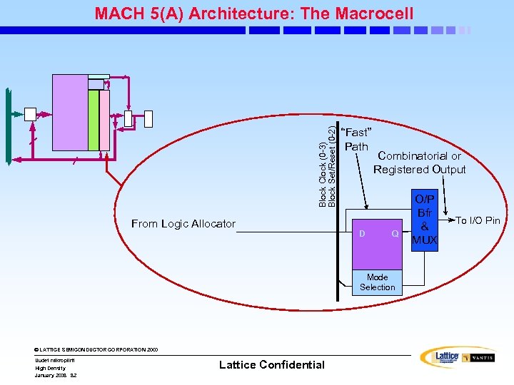 Block Clock (0 -3) Block Set/Reset (0 -2) MACH 5(A) Architecture: The Macrocell From Logic Allocator “Fast” Path D Combinatorial or Registered Output Q Mode Selection © LATTICE SEMICONDUCTOR CORPORATION 2000 Uudet mikropiirit High Density January 2008 82 Lattice Confidential O/P Bfr & MUX To I/O Pin
 MACH 5(A) Architecture: Macrocell Modes • Combinatorial • D-Type flip-flop • Latch • T-Type flip-flop (synthesized) • J-K flip-flop (synthesized) • S-R flip-flop (synthesized) © LATTICE SEMICONDUCTOR CORPORATION 2000 Uudet mikropiirit High Density January 2008 83 Lattice Confidential
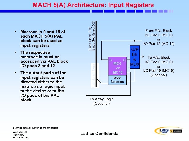 • Macrocells 0 and 15 of each MACH 5(A) PAL block can be used as input registers • The respective macrocells must be accessed via PAL block I/O pads 3 and 12 • The output ports of the input registers can be directed either to the matrix as a logic input to the device or to the I/O pads of the PAL block Block Clock (0 -3) Block Set/Reset (0 -2) MACH 5(A) Architecture: Input Registers From PAL Block I/O Pad 3 (MC 0) or I/O Pad 12 (MC 15) D MC 0 or MC 15 Mode Selection To Array Logic (Optional) © LATTICE SEMICONDUCTOR CORPORATION 2000 Uudet mikropiirit High Density January 2008 84 Q Lattice Confidential O/P Bfr & MUX To PAL Block I/O Pad 0 (MC 0) or I/O Pad 15 (MC 15) (Optional)
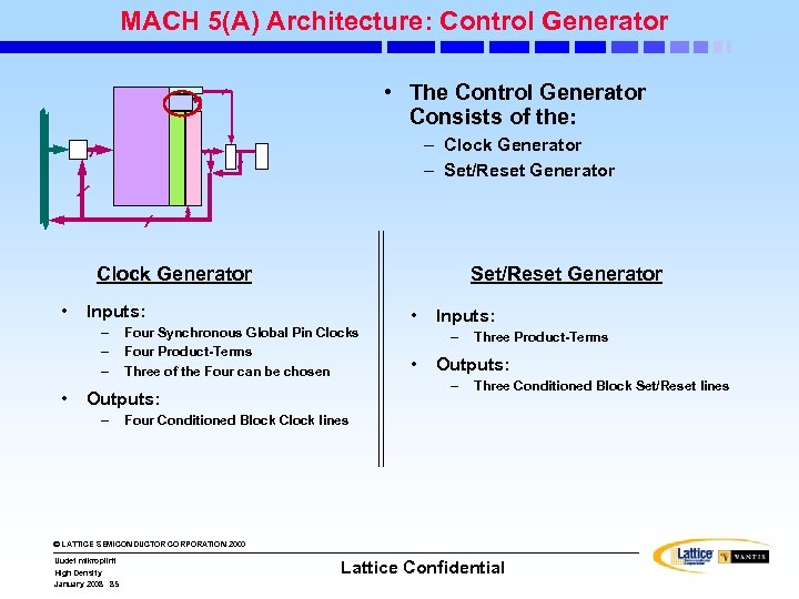 MACH 5(A) Architecture: Control Generator • The Control Generator Consists of the: – Clock Generator – Set/Reset Generator Clock Generator • Inputs: – – – • Set/Reset Generator Four Synchronous Global Pin Clocks Four Product-Terms Three of the Four can be chosen Outputs: – • Inputs: – • Three Product-Terms Outputs: – Three Conditioned Block Set/Reset lines Four Conditioned Block Clock lines © LATTICE SEMICONDUCTOR CORPORATION 2000 Uudet mikropiirit High Density January 2008 85 Lattice Confidential
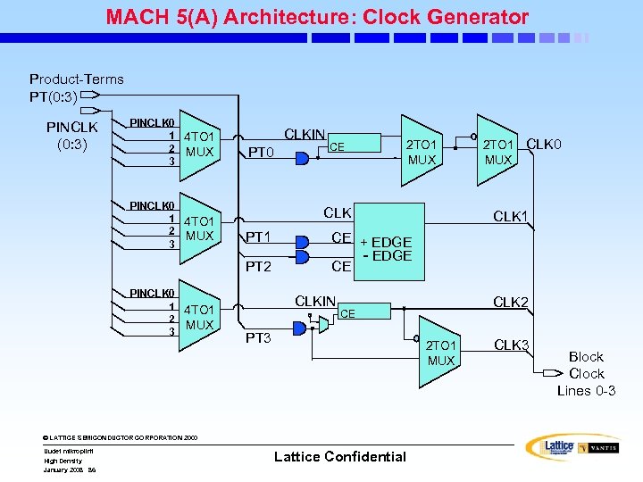 MACH 5(A) Architecture: Clock Generator Product-Terms PT(0: 3) PINCLK 0 1 4 TO 1 2 MUX 3 CLKIN PT 0 2 TO 1 MUX CLK PT 1 PT 2 PINCLK 0 1 4 TO 1 2 MUX 3 CE High Density January 2008 86 CLK 1 CE + EDGE - EDGE CE CLKIN CLK 2 CE PT 3 2 TO 1 MUX © LATTICE SEMICONDUCTOR CORPORATION 2000 Uudet mikropiirit 2 TO 1 CLK 0 MUX Lattice Confidential CLK 3 Block Clock Lines 0 -3
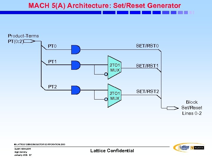 MACH 5(A) Architecture: Set/Reset Generator Product-Terms PT(0: 2) SET/RST 0 PT 1 2 TO 1 MUX PT 2 2 TO 1 MUX © LATTICE SEMICONDUCTOR CORPORATION 2000 Uudet mikropiirit High Density January 2008 87 Lattice Confidential SET/RST 1 SET/RST 2 Block Set/Reset Lines 0 -2
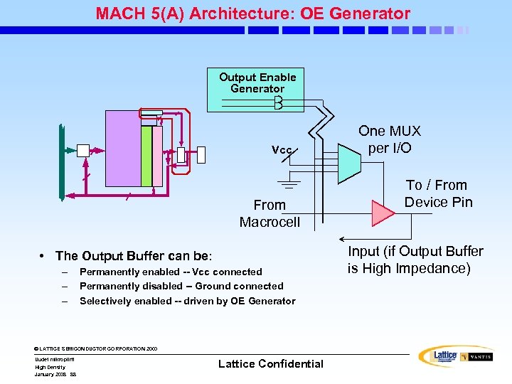 MACH 5(A) Architecture: OE Generator Output Enable Generator Vcc From Macrocell • The Output Buffer can be: – – – Permanently enabled -- Vcc connected Permanently disabled -- Ground connected Selectively enabled -- driven by OE Generator © LATTICE SEMICONDUCTOR CORPORATION 2000 Uudet mikropiirit High Density January 2008 88 Lattice Confidential One MUX per I/O To / From Device Pin Input (if Output Buffer is High Impedance)
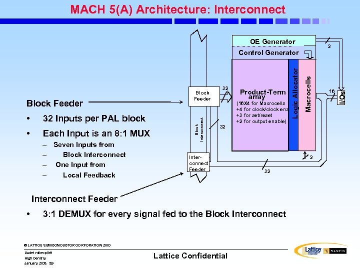 MACH 5(A) Architecture: Interconnect OE Generator • • 32 Inputs per PAL block Each Input is an 8: 1 MUX – Seven Inputs from – Block Interconnect – One Input from – Local Feedback Block Interconnect 32 32 Interconnect Feeder Product-Term array (16 X 4 for Macrocells +4 for clock/clock enable +3 for set/reset +2 for output enable) 2 32 Interconnect Feeder • 3: 1 DEMUX for every signal fed to the Block Interconnect © LATTICE SEMICONDUCTOR CORPORATION 2000 Uudet mikropiirit High Density January 2008 89 Lattice Confidential Macrocells Block Feeder Logic Allocator Control Generator 16 I/Os 2
 MACH 5(A) Segment Interconnect Lines • Block interconnect lines connect to the segment interconnect lines through a 3 to 1 demultiplexor • The difference between any two MACH 5(A) densities: – The number of segments – The number of Segment Interconnect Lines: » M 5(A)-128 has 128 lines » M 5(A)-192 has 128 lines » M 5(A)-256 has 128 lines » M 5(A)-320 has 152 lines » M 5(A)-384 has 164 lines » M 5(A)-512 has 192 lines © LATTICE SEMICONDUCTOR CORPORATION 2000 Uudet mikropiirit High Density January 2008 90 Lattice Confidential
 MACH 5(A) Timing Model: Introduction • The MACH 5(A) Timing Model is used to estimate delay that a signal incurs as it passes through the device • Different input types are subject to different delay factors owing to the different routing and treatments afforded them • Different input types shown in the timing model are: – – Regular inputs and inputs fed back from intern macrocell outputs Pin (“global”) clock inputs PT clocks and enables for flip-flops and latches Inputs directly connected to input registers. © LATTICE SEMICONDUCTOR CORPORATION 2000 Uudet mikropiirit High Density January 2008 91 Lattice Confidential
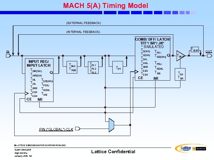 MACH 5(A) Timing Model (EXTERNAL FEEDBACK) (INTERNAL FEEDBACK) IN INPUT REG/ INPUT LATCH TSIR(S/A) Q THIR(S/A) TSIL TCO(S/A)i THIL T PDILi TSRR TGOAL TCES TCEH TSRi CE SR TBLK TSEG TPL 1 TPL 2 TPL 3 TPT COMB/ DFF/ LATCH/ TFF*/ SR*/ JK* * SIMULATED TS(S/A) T PD i TH(S/A) TCO(S/A)i Q TSAL THIAL TPDLi TSRR TGOAL TCES TSRi T CE PIN (“GLOBAL”) CLK © LATTICE SEMICONDUCTOR CORPORATION 2000 Uudet mikropiirit High Density January 2008 92 CEH Lattice Confidential SR TSLW TBUF TEA TER OUT
 MACH 5(A) Timing Model: Parameters • Questions related to the application of the MACH 5(A) Timing Model delay parameters might be as follows for a “regular” input: – Does the path cross into a second PAL block within the same segment? » If so, add the t. BLK delay constant – Does the path cross into a PAL block of a different segment? » If so, add the t. SEG delay constant – Does path involve PAL blocks programmed for reduced power? » If so, apply the appropriate t. PLx delay constant(s) • If none, some or all of the above apply, consider the appropriate constants and proceed on the path to the “Logic” delay constants © LATTICE SEMICONDUCTOR CORPORATION 2000 Uudet mikropiirit High Density January 2008 93 Lattice Confidential
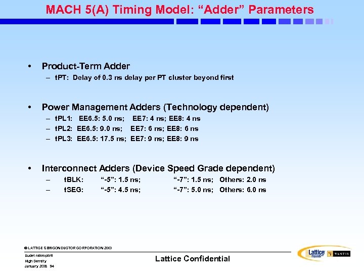 MACH 5(A) Timing Model: “Adder” Parameters • Product-Term Adder – t. PT: Delay of 0. 3 ns delay per PT cluster beyond first • Power Management Adders (Technology dependent) – t. PL 1: EE 6. 5: 5. 0 ns; EE 7: 4 ns; EE 8: 4 ns – t. PL 2: EE 6. 5: 9. 0 ns; EE 7: 6 ns; EE 8: 6 ns – t. PL 3: EE 6. 5: 17. 5 ns; EE 7: 9 ns; EE 8: 9 ns • Interconnect Adders (Device Speed Grade dependent) – – t. BLK: t. SEG: “-5”: 1. 5 ns; “-5”: 4. 5 ns; “-7”: 1. 5 ns; Others: 2. 0 ns “-7”: 5. 0 ns; Others: 6. 0 ns © LATTICE SEMICONDUCTOR CORPORATION 2000 Uudet mikropiirit High Density January 2008 94 Lattice Confidential
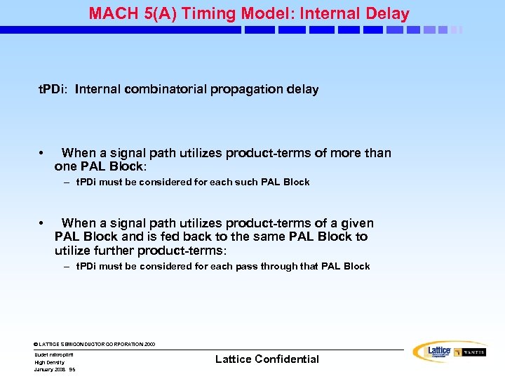 MACH 5(A) Timing Model: Internal Delay t. PDi: Internal combinatorial propagation delay • When a signal path utilizes product-terms of more than one PAL Block: – t. PDi must be considered for each such PAL Block • When a signal path utilizes product-terms of a given PAL Block and is fed back to the same PAL Block to utilize further product-terms: – t. PDi must be considered for each pass through that PAL Block © LATTICE SEMICONDUCTOR CORPORATION 2000 Uudet mikropiirit High Density January 2008 95 Lattice Confidential
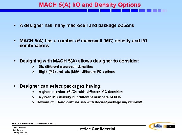 MACH 5(A) I/O and Density Options • A designer has many macrocell and package options • MACH 5(A) has a number of macrocell (MC) density and I/O combinations • Designing with MACH 5(A) allows designer to consider: » » Six different macrocell densities Eight (M 5) and six (M 5 A) different I/O options • Designer can select packages having: » A given number of I/Os with different MC densities » A given MC density but different numbers of I/Os » Beware of “Bond-out” issues with device/package migrations!! © LATTICE SEMICONDUCTOR CORPORATION 2000 Uudet mikropiirit High Density January 2008 96 Lattice Confidential
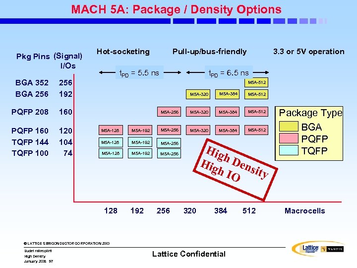 MACH 5 A: Package / Density Options Pkg Pins (Signal) I/Os BGA 352 BGA 256 160 PQFP 160 TQFP 144 TQFP 100 120 104 74 Pull-up/bus-friendly t. PD = 5. 5 ns 256 192 PQFP 208 Hot-socketing t. PD = 6. 5 ns M 5 A-512 M 5 A-320 M 5 A-384 M 5 A-512 M 5 A-256 M 5 A-320 M 5 A-384 M 5 A-512 M 5 A-128 M 5 A-192 M 5 A-256 128 192 256 Hig h Dens h IO ity 320 384 © LATTICE SEMICONDUCTOR CORPORATION 2000 Uudet mikropiirit High Density January 2008 97 3. 3 or 5 V operation Lattice Confidential 512 Package Type BGA PQFP TQFP Macrocells
 Mach 4 © LATTICE SEMICONDUCTOR CORPORATION 2000 Uudet mikropiirit High Density January 2008 98 Lattice Confidential
 MACH 4(A) CPLD Family Overview • Training Module covers: • MACH 4(A) Family performance features and characteristics • MACH 4(A) Architecture – MACH 4(A) internal “components” and subsystems • MACH 4(A) Speed. Locking. TM © LATTICE SEMICONDUCTOR CORPORATION 2000 Uudet mikropiirit High Density January 2008 99 Lattice Confidential
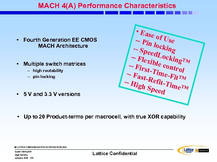 MACH 4(A) Performance Characteristics • Fourth Generation EE CMOS MACH Architecture • Multiple switch matrices – high routability – pin locking • 5 V and 3. 3 V versions • Eas e of U se -- Pin -- Sp locking ee -- Fle d. Lockin TM g x -- Fir ible contr s ol -- Fa t-Time-F TM it st-Re f -- Hi gh Sp it-Time TM eed • Up to 20 Product-terms per macrocell, with true XOR capability © LATTICE SEMICONDUCTOR CORPORATION 2000 Uudet mikropiirit High Density January 2008 100 Lattice Confidential
 MACH 4(A) Performance Characteristics • Dedicated input registers/latches • Power management feature – PAL block-based programmable power-down mode • Flexible clocking – Four global clocks with selectable edges – Synchronous or Asynchronous mode for each macrocell © LATTICE SEMICONDUCTOR CORPORATION 2000 Uudet mikropiirit High Density January 2008 101 Lattice Confidential
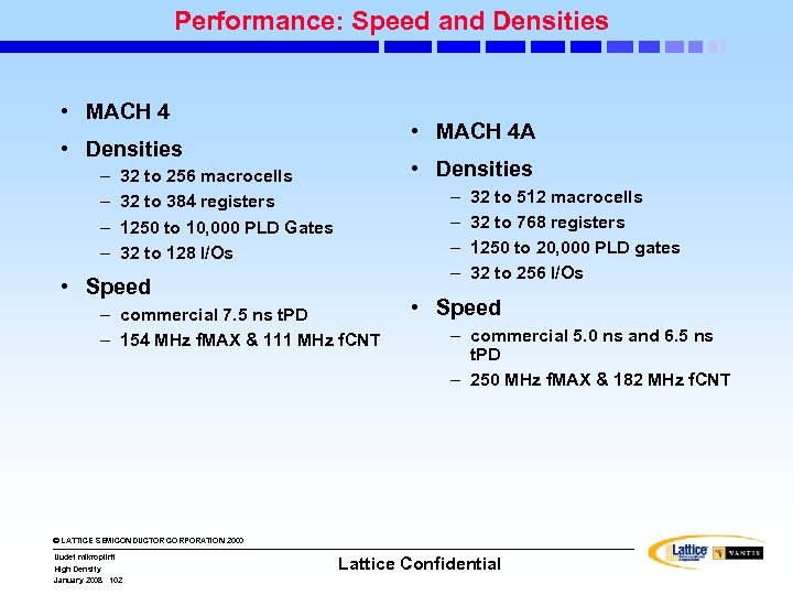 Performance: Speed and Densities • MACH 4 A • Densities – – • Densities 32 to 256 macrocells 32 to 384 registers 1250 to 10, 000 PLD Gates 32 to 128 I/Os – – • Speed – commercial 7. 5 ns t. PD – 154 MHz f. MAX & 111 MHz f. CNT 32 to 512 macrocells 32 to 768 registers 1250 to 20, 000 PLD gates 32 to 256 I/Os • Speed – commercial 5. 0 ns and 6. 5 ns t. PD – 250 MHz f. MAX & 182 MHz f. CNT © LATTICE SEMICONDUCTOR CORPORATION 2000 Uudet mikropiirit High Density January 2008 102 Lattice Confidential
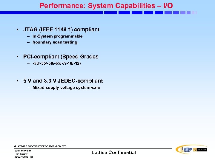 Performance: System Capabilities – I/O • JTAG (IEEE 1149. 1) compliant – In-System programmable – boundary scan testing • PCI-compliant (Speed Grades – -50/-55/-60/-65/-7/-10/-12) • 5 V and 3. 3 V JEDEC-compliant – Mixed supply voltage system-safe © LATTICE SEMICONDUCTOR CORPORATION 2000 Uudet mikropiirit High Density January 2008 103 Lattice Confidential
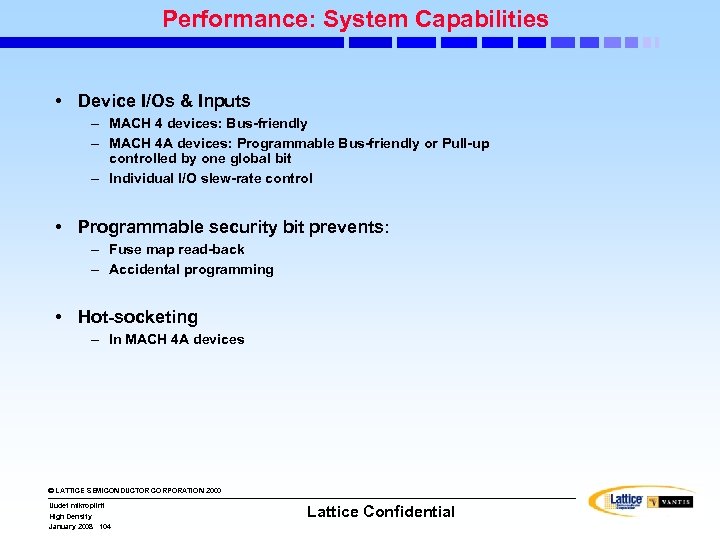 Performance: System Capabilities • Device I/Os & Inputs – MACH 4 devices: Bus-friendly – MACH 4 A devices: Programmable Bus-friendly or Pull-up controlled by one global bit – Individual I/O slew-rate control • Programmable security bit prevents: – Fuse map read-back – Accidental programming • Hot-socketing – In MACH 4 A devices © LATTICE SEMICONDUCTOR CORPORATION 2000 Uudet mikropiirit High Density January 2008 104 Lattice Confidential
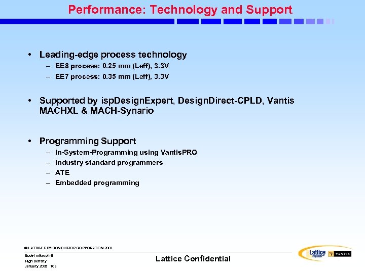 Performance: Technology and Support • Leading-edge process technology – EE 8 process: 0. 25 mm (Leff), 3. 3 V – EE 7 process: 0. 35 mm (Leff), 3. 3 V • Supported by isp. Design. Expert, Design. Direct-CPLD, Vantis MACHXL & MACH-Synario • Programming Support – – In-System-Programming using Vantis. PRO Industry standard programmers ATE Embedded programming © LATTICE SEMICONDUCTOR CORPORATION 2000 Uudet mikropiirit High Density January 2008 105 Lattice Confidential
 MACH 4(A) Architecture Overview • Architecture types – Based on macrocell to I/O ratio – 1: 1 Architecture and 2: 1 Architecture • Multiple switch matrices – Input, Central and Output • PAL blocks – – – Product-Term arrays Logic allocators Multimode macrocells I/O cells Control and OE generators © LATTICE SEMICONDUCTOR CORPORATION 2000 Uudet mikropiirit High Density January 2008 106 Lattice Confidential
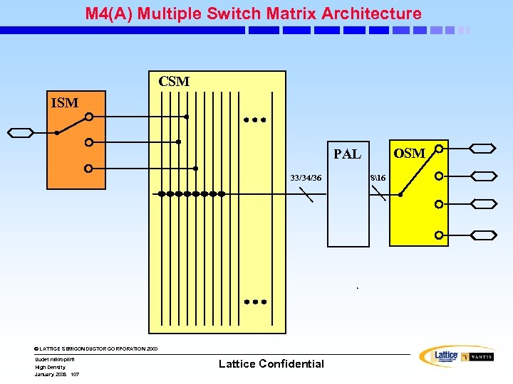 M 4(A) Multiple Switch Matrix Architecture CSM ISM OSM PAL 33/34/36 © LATTICE SEMICONDUCTOR CORPORATION 2000 Uudet mikropiirit High Density January 2008 107 Lattice Confidential 816
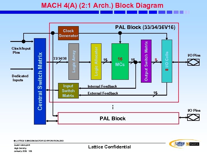 MACH 4(A) (2: 1 Arch. ) Block Diagram Input Switch Matrix 16 MCs 16 16 External Feedback . . . © LATTICE SEMICONDUCTOR CORPORATION 2000 High Density January 2008 108 I/O Pins Internal Feedback PAL Block Uudet mikropiirit 8 8 I/O Cells Logic Array 33/34/36 Logic Allocator Dedicated Inputs Central Switch Matrix Clock/Input Pins Output Switch Matrix PAL Block (33/34/36 V 16) Clock Generator Lattice Confidential 16 I/O Pins
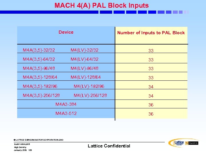 MACH 4(A) PAL Block Inputs Device Number of Inputs to PAL Block M 4 A(3, 5)-32/32 M 4(LV)-32/32 33 M 4 A(3, 5)-64/32 M 4(LV)-64/32 33 M 4 A(3, 5)-96/48 M 4(LV)-96/48 33 M 4 A(3, 5)-128/64 M 4(LV)-128/64 33 M 4 A(3, 5)-192/96 M 4(LV)-192/96 34 M 4 A(3, 5)-256/128 M 4(LV)-256/128 34 M 4 A 3 -384 36 M 4 A 3 -512 36 © LATTICE SEMICONDUCTOR CORPORATION 2000 Uudet mikropiirit High Density January 2008 109 Lattice Confidential
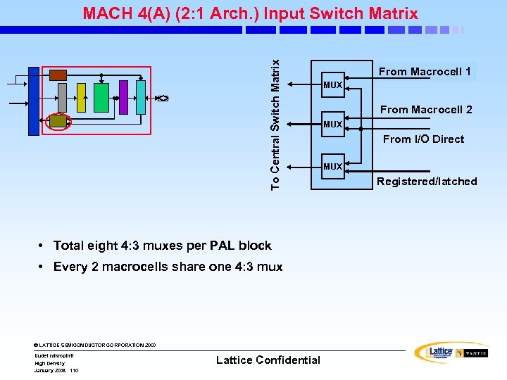 To Central Switch Matrix MACH 4(A) (2: 1 Arch. ) Input Switch Matrix • Total eight 4: 3 muxes per PAL block • Every 2 macrocells share one 4: 3 mux © LATTICE SEMICONDUCTOR CORPORATION 2000 Uudet mikropiirit High Density January 2008 110 Lattice Confidential From Macrocell 1 MUX From Macrocell 2 MUX From I/O Direct MUX Registered/latched
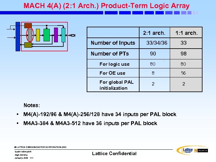 MACH 4(A) (2: 1 Arch. ) Product-Term Logic Array 2: 1 arch. Number of Inputs 1: 1 arch. 33/34/36 33 Number of PTs 90 98 For logic use 80 80 For OE use 8 16 For global PAL initialization 2 2 Notes: • M 4(A)-192/96 & M 4(A)-256/128 have 34 inputs per PAL block • M 4 A 3 -384 & M 4 A 3 -512 have 36 inputs per PAL block © LATTICE SEMICONDUCTOR CORPORATION 2000 Uudet mikropiirit High Density January 2008 111 Lattice Confidential
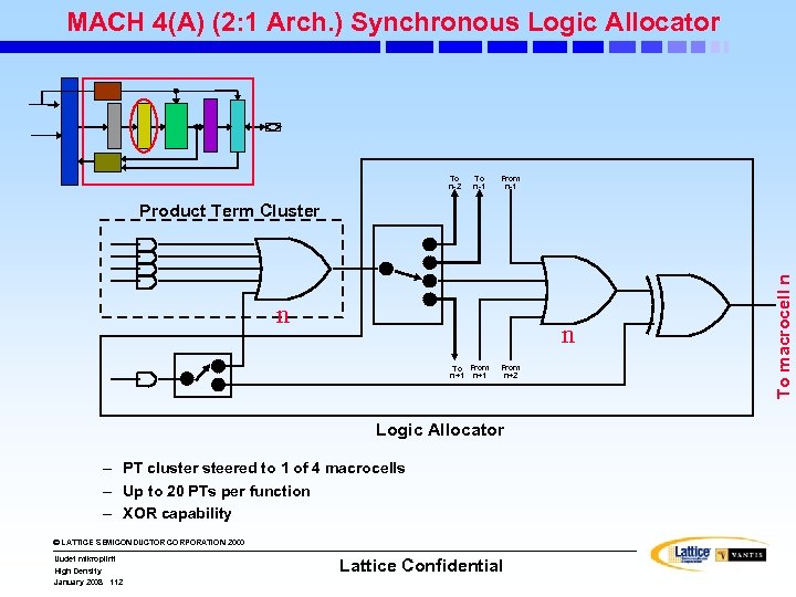 MACH 4(A) (2: 1 Arch. ) Synchronous Logic Allocator To n-2 To n-1 From n-1 n n To From n+1 From n+2 Logic Allocator – PT cluster steered to 1 of 4 macrocells – Up to 20 PTs per function – XOR capability © LATTICE SEMICONDUCTOR CORPORATION 2000 Uudet mikropiirit High Density January 2008 112 Lattice Confidential To macrocell n Product Term Cluster
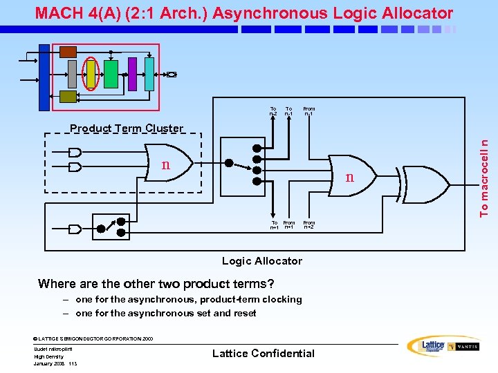 MACH 4(A) (2: 1 Arch. ) Asynchronous Logic Allocator To n-2 To n-1 From n-1 n n To From n+1 From n+2 Logic Allocator Where are the other two product terms? – one for the asynchronous, product-term clocking – one for the asynchronous set and reset © LATTICE SEMICONDUCTOR CORPORATION 2000 Uudet mikropiirit High Density January 2008 113 Lattice Confidential To macrocell n Product Term Cluster
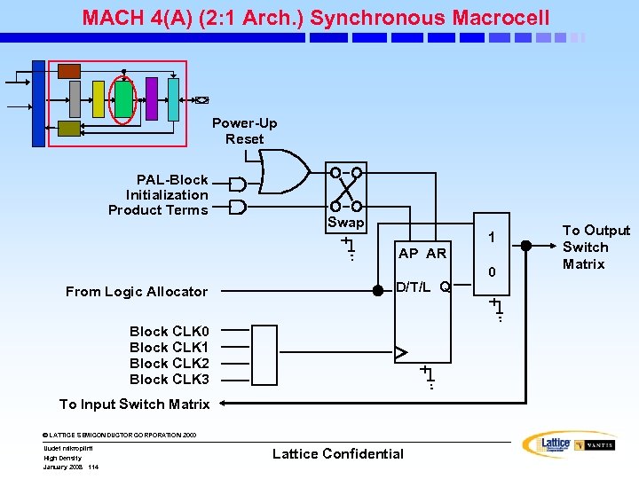 MACH 4(A) (2: 1 Arch. ) Synchronous Macrocell Power-Up Reset PAL-Block Initialization Product Terms Swap AP AR From Logic Allocator D/T/L Q Block CLK 0 Block CLK 1 Block CLK 2 Block CLK 3 To Input Switch Matrix © LATTICE SEMICONDUCTOR CORPORATION 2000 Uudet mikropiirit High Density January 2008 114 Lattice Confidential 1 0 To Output Switch Matrix
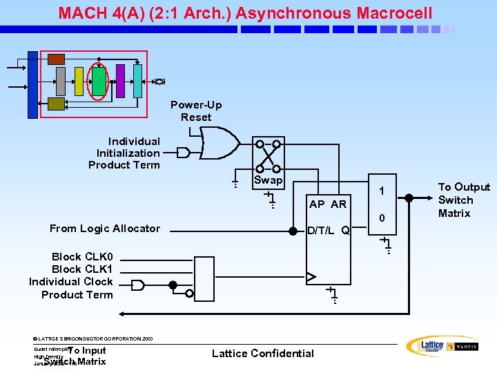 MACH 4(A) (2: 1 Arch. ) Asynchronous Macrocell Power-Up Reset Individual Initialization Product Term Swap 1 AP AR From Logic Allocator 0 D/T/L Q Block CLK 0 Block CLK 1 Individual Clock Product Term © LATTICE SEMICONDUCTOR CORPORATION 2000 To Input Switch Matrix Uudet mikropiirit High Density January 2008 115 Lattice Confidential To Output Switch Matrix
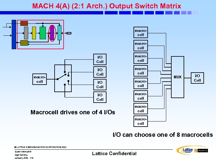 MACH 4(A) (2: 1 Arch. ) Output Switch Matrix macrocell I/O Cell macrocell Macrocell drives one of 4 I/Os MUX I/O Cell macrocell I/O can choose one of 8 macrocells © LATTICE SEMICONDUCTOR CORPORATION 2000 Uudet mikropiirit High Density January 2008 116 Lattice Confidential
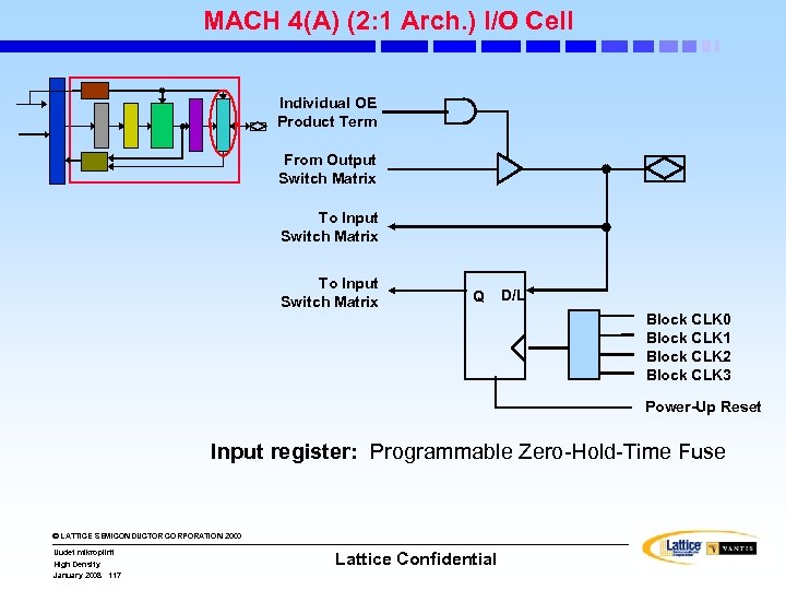 MACH 4(A) (2: 1 Arch. ) I/O Cell Individual OE Product Term From Output Switch Matrix To Input Switch Matrix Q D/L Block CLK 0 Block CLK 1 Block CLK 2 Block CLK 3 Power-Up Reset Input register: Programmable Zero-Hold-Time Fuse © LATTICE SEMICONDUCTOR CORPORATION 2000 Uudet mikropiirit High Density January 2008 117 Lattice Confidential
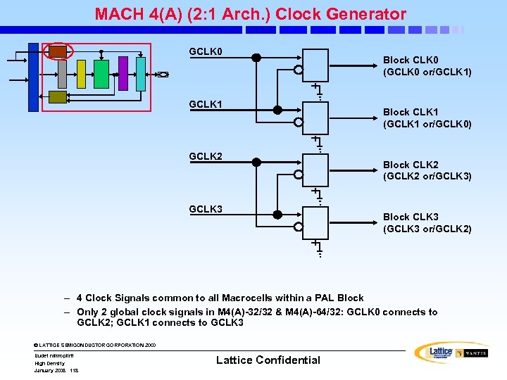 MACH 4(A) (2: 1 Arch. ) Clock Generator GCLK 0 GCLK 1 GCLK 2 GCLK 3 Block CLK 0 (GCLK 0 or/GCLK 1) Block CLK 1 (GCLK 1 or/GCLK 0) Block CLK 2 (GCLK 2 or/GCLK 3) Block CLK 3 (GCLK 3 or/GCLK 2) – 4 Clock Signals common to all Macrocells within a PAL Block – Only 2 global clock signals in M 4(A)-32/32 & M 4(A)-64/32: GCLK 0 connects to GCLK 2; GCLK 1 connects to GCLK 3 © LATTICE SEMICONDUCTOR CORPORATION 2000 Uudet mikropiirit High Density January 2008 118 Lattice Confidential
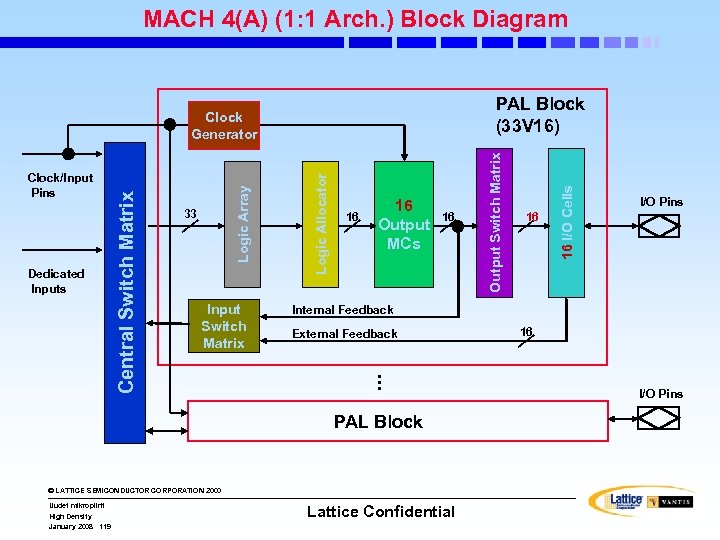 MACH 4(A) (1: 1 Arch. ) Block Diagram Input Switch Matrix 16 16 Output MCs 16 External Feedback . . . © LATTICE SEMICONDUCTOR CORPORATION 2000 High Density January 2008 119 I/O Pins Internal Feedback PAL Block Uudet mikropiirit 16 16 I/O Cells Logic Array 33 Logic Allocator Dedicated Inputs Central Switch Matrix Clock/Input Pins Output Switch Matrix PAL Block (33 V 16) Clock Generator Lattice Confidential 16 I/O Pins
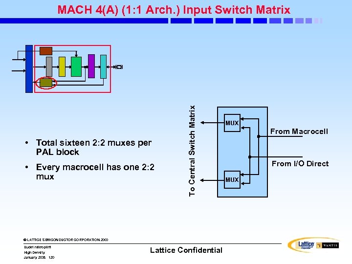 • Total sixteen 2: 2 muxes per PAL block • Every macrocell has one 2: 2 mux To Central Switch Matrix MACH 4(A) (1: 1 Arch. ) Input Switch Matrix © LATTICE SEMICONDUCTOR CORPORATION 2000 Uudet mikropiirit High Density January 2008 120 Lattice Confidential MUX From Macrocell From I/O Direct MUX
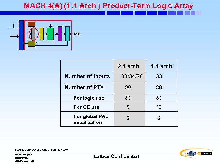 MACH 4(A) (1: 1 Arch. ) Product-Term Logic Array 2: 1 arch. Number of Inputs 33/34/36 1: 1 arch. 33 Number of PTs 90 98 For logic use 80 80 For OE use 8 16 For global PAL initialization 2 2 © LATTICE SEMICONDUCTOR CORPORATION 2000 Uudet mikropiirit High Density January 2008 121 Lattice Confidential
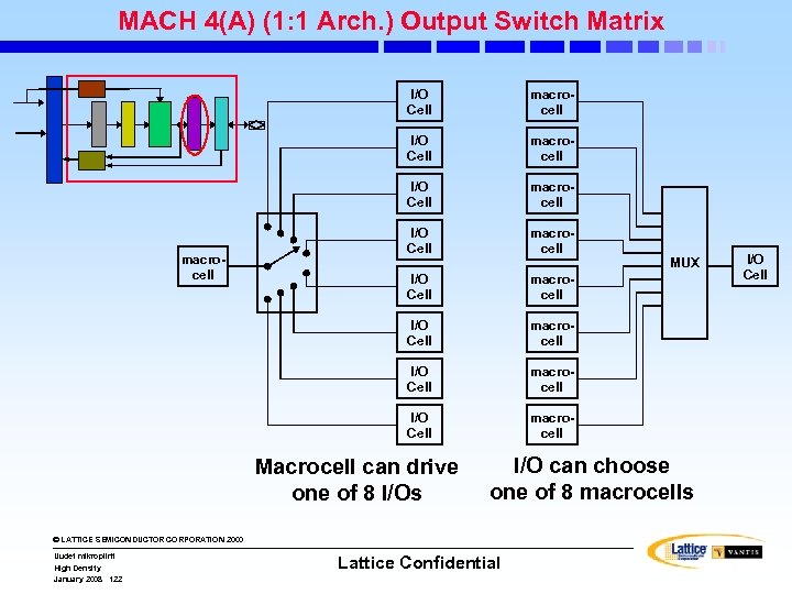 MACH 4(A) (1: 1 Arch. ) Output Switch Matrix I/O Cell macrocell I/O Cell macrocell macrocell Macrocell can drive one of 8 I/Os I/O can choose one of 8 macrocells © LATTICE SEMICONDUCTOR CORPORATION 2000 Uudet mikropiirit High Density January 2008 122 MUX Lattice Confidential I/O Cell
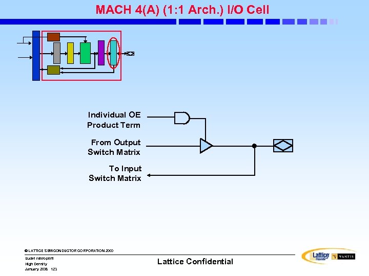 MACH 4(A) (1: 1 Arch. ) I/O Cell Individual OE Product Term From Output Switch Matrix To Input Switch Matrix © LATTICE SEMICONDUCTOR CORPORATION 2000 Uudet mikropiirit High Density January 2008 123 Lattice Confidential
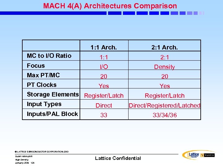 MACH 4(A) Architectures Comparison 1: 1 Arch. 2: 1 Arch. MC to I/O Ratio 1: 1 2: 1 Focus I/O Density Max PT/MC 20 20 PT Clocks Yes Storage Elements Register/Latch Input Types Direct/Registered/Latched Inputs/PAL Block 33 33/34/36 © LATTICE SEMICONDUCTOR CORPORATION 2000 Uudet mikropiirit High Density January 2008 124 Lattice Confidential
 MACH 4(A) Speed. Locking. TM • Speed. Locking assures guaranteed timing – independent of the path taken through device • No expander or PT adders required • Ensures complete predictability • All MACH 4(A) devices have Speed. Locking © LATTICE SEMICONDUCTOR CORPORATION 2000 Uudet mikropiirit High Density January 2008 125 Lattice Confidential
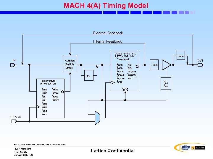 MACH 4(A) Timing Model External Feedback Internal Feedback IN COMB / DFF / TFF / LATCH / SR* / JK* * simulated Central Switch Matrix t. PL INPUT REG/ INPUT LATCH PIN CLK t. SIRS t. HIRS t. SIL t. HIL t. SIRZ t. HIRZ t. SILZ t. HILZ t. PDILi t. ICOSi t. IGOSi t. PDILZi Q t. SS(T) t. SA(T) t. H(S/A) t. S(S/A)L t. H(S/A)L t. SRR t. PDi t. PDLi Q t. CO(S/A)i t. GO(S/A)i t. SRi S/R © LATTICE SEMICONDUCTOR CORPORATION 2000 Uudet mikropiirit High Density January 2008 126 Lattice Confidential t. SLW OUT t. BUF t. EA t. ER
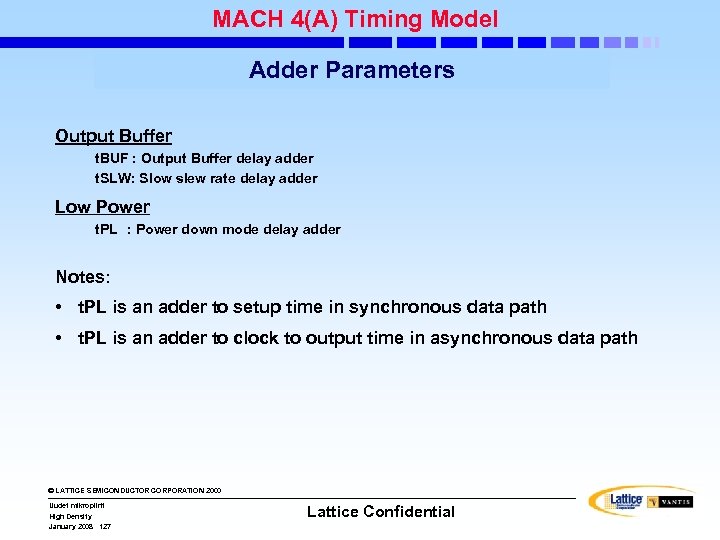 MACH 4(A) Timing Model Adder Parameters Output Buffer t. BUF : Output Buffer delay adder t. SLW: Slow slew rate delay adder Low Power t. PL : Power down mode delay adder Notes: • t. PL is an adder to setup time in synchronous data path • t. PL is an adder to clock to output time in asynchronous data path © LATTICE SEMICONDUCTOR CORPORATION 2000 Uudet mikropiirit High Density January 2008 127 Lattice Confidential
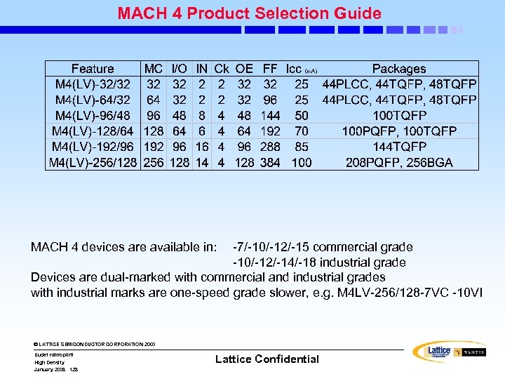 MACH 4 Product Selection Guide MACH 4 devices are available in: -7/-10/-12/-15 commercial grade -10/-12/-14/-18 industrial grade Devices are dual-marked with commercial and industrial grades with industrial marks are one-speed grade slower, e. g. M 4 LV-256/128 -7 VC -10 VI © LATTICE SEMICONDUCTOR CORPORATION 2000 Uudet mikropiirit High Density January 2008 128 Lattice Confidential
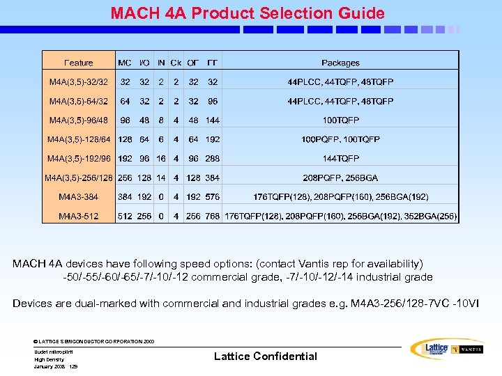 MACH 4 A Product Selection Guide MACH 4 A devices have following speed options: (contact Vantis rep for availability) -50/-55/-60/-65/-7/-10/-12 commercial grade, -7/-10/-12/-14 industrial grade Devices are dual-marked with commercial and industrial grades e. g. M 4 A 3 -256/128 -7 VC -10 VI © LATTICE SEMICONDUCTOR CORPORATION 2000 Uudet mikropiirit High Density January 2008 129 Lattice Confidential
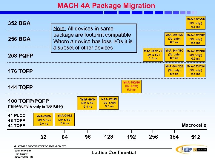 MACH 4 A Package Migration 352 BGA Note: All devices in same package are footprint compatible. Where a device has less I/Os it is a subset of other devices M 4 A-512/256 (3 V only) 6. 5 ns 208 PQFP M 4 A-256/128 (3 V & 5 V) 5. 0 ns 176 TQFP 100 TQFP/PQFP (*M 4 A-96/48 is only in 100 TQFP) M 4 A-32/32 (3 V & 5 V) 5. 0 ns 64 *M 4 A-96/48 (3 V & 5 V) 5. 0 ns M 4 A-512/128 (3 V only) 6. 5 ns M 4 A-128/64 (3 V & 5 V) 5. 0 ns Macrocells 96 128 192 © LATTICE SEMICONDUCTOR CORPORATION 2000 High Density January 2008 130 M 4 A-512/160 (3 V only) 6. 5 ns M 4 A-64/32 (3 V & 5 V) 5. 0 ns 32 Uudet mikropiirit M 4 A-384/160 (3 V only) 6. 5 ns M 4 A-192/96 (3 V & 5 V) 5. 0 ns 144 TQFP 44 PLCC 48 TQFP 44 TQFP M 4 A-512/192 (3 V only) 6. 5 ns M 4 A-384/128 (3 V only) 6. 5 ns 256 BGA M 4 A-384/192 (3 V only) 6. 5 ns Lattice Confidential 256 384 512
 isp. LSI and Mach Comparison © LATTICE SEMICONDUCTOR CORPORATION 2000 Uudet mikropiirit High Density January 2008 131 Lattice Confidential
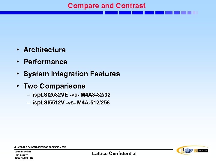 Compare and Contrast • Architecture • Performance • System Integration Features • Two Comparisons – isp. LSI 2032 VE -vs- M 4 A 3 -32/32 – isp. LSI 5512 V -vs- M 4 A-512/256 © LATTICE SEMICONDUCTOR CORPORATION 2000 Uudet mikropiirit High Density January 2008 132 Lattice Confidential
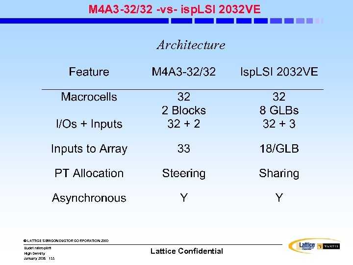 M 4 A 3 -32/32 -vs- isp. LSI 2032 VE Architecture © LATTICE SEMICONDUCTOR CORPORATION 2000 Uudet mikropiirit High Density January 2008 133 Lattice Confidential
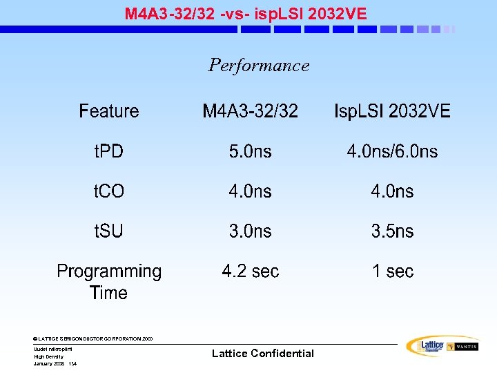 M 4 A 3 -32/32 -vs- isp. LSI 2032 VE Performance © LATTICE SEMICONDUCTOR CORPORATION 2000 Uudet mikropiirit High Density January 2008 134 Lattice Confidential
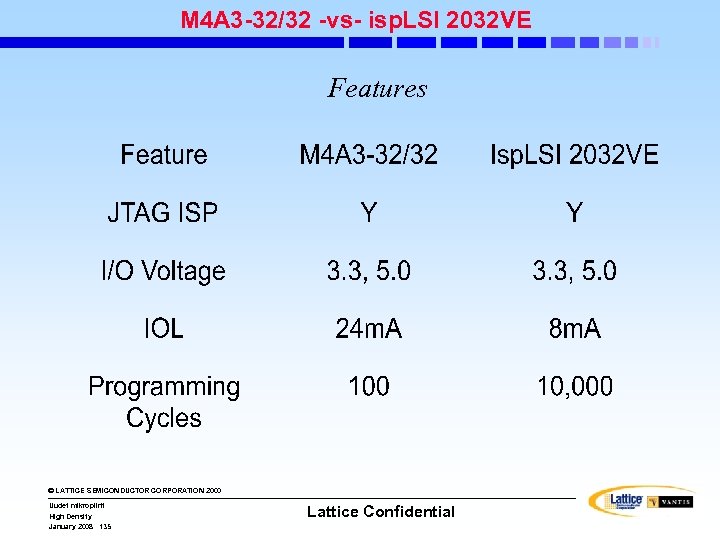 M 4 A 3 -32/32 -vs- isp. LSI 2032 VE Features © LATTICE SEMICONDUCTOR CORPORATION 2000 Uudet mikropiirit High Density January 2008 135 Lattice Confidential
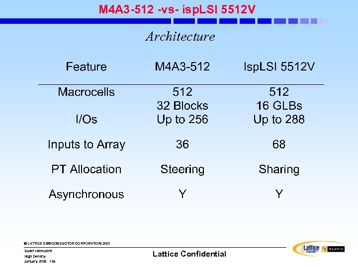 M 4 A 3 -512 -vs- isp. LSI 5512 V Architecture © LATTICE SEMICONDUCTOR CORPORATION 2000 Uudet mikropiirit High Density January 2008 136 Lattice Confidential
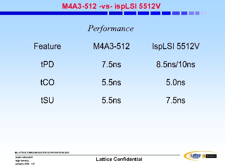 M 4 A 3 -512 -vs- isp. LSI 5512 V Performance © LATTICE SEMICONDUCTOR CORPORATION 2000 Uudet mikropiirit High Density January 2008 137 Lattice Confidential
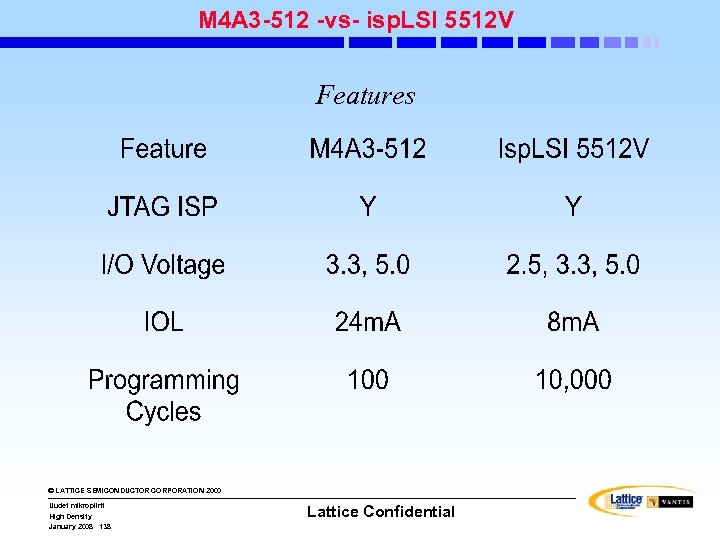 M 4 A 3 -512 -vs- isp. LSI 5512 V Features © LATTICE SEMICONDUCTOR CORPORATION 2000 Uudet mikropiirit High Density January 2008 138 Lattice Confidential
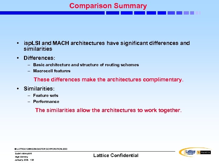 Comparison Summary • isp. LSI and MACH architectures have significant differences and similarities • Differences: – Basic architecture and structure of routing schemes – Macrocell features These differences make the architectures complimentary. • Similarities: – Feature sets – Performance The similarities allow the architectures to work together. © LATTICE SEMICONDUCTOR CORPORATION 2000 Uudet mikropiirit High Density January 2008 139 Lattice Confidential
 ISP © LATTICE SEMICONDUCTOR CORPORATION 2000 Uudet mikropiirit High Density January 2008 140 Lattice Confidential
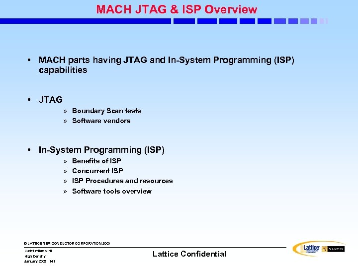 MACH JTAG & ISP Overview • MACH parts having JTAG and In-System Programming (ISP) capabilities • JTAG » Boundary Scan tests » Software vendors • In-System Programming (ISP) » » Benefits of ISP Concurrent ISP Procedures and resources Software tools overview © LATTICE SEMICONDUCTOR CORPORATION 2000 Uudet mikropiirit High Density January 2008 141 Lattice Confidential
 JTAG 5 -Pin Standard and Vantis 6 -Pin Interface • JTAG 5 -Pin Standard programming port adds an optional TRST* (Test Reset) pin: – used to asynchronously reset the TAP controller – active LOW -- connect to Vcc/HIGH when not used • Vantis 6 -Pin Interface adds an ENABLE* pin for some MACH 4 xx parts: – Used for programming – Active LOW -- connect to GND/LOW if not required – Devices using the Vantis 6 -pin port are M 4 -96/96, M 4 -128 and M 4 -256 only © LATTICE SEMICONDUCTOR CORPORATION 2000 Uudet mikropiirit High Density January 2008 142 Lattice Confidential
 MACH Devices with the JTAG Feature • MACH JTAG-ISP parts with JTAG 4 -pin standard: – – – – MACH 1 XXSP** MACH 2 XXSP** MACH 4 -32 MACH 4 -64 MACH 4 -96/48 MACH 4 -192 MACH 5 XX • JTAG-ISP parts with Vantis 6 -pin programming port: – MACH 4 -96/96 – MACH 4 -128 – MACH 4 -256 • To comply with JTAG 4 -pin standard, connect TRST* to HIGH and ENABLE* to LOW ** MACH 1 and MACH 2 Devices are JTAG-Compatible but not JTAG-Compliant © LATTICE SEMICONDUCTOR CORPORATION 2000 Uudet mikropiirit High Density January 2008 143 Lattice Confidential
 JTAG Instructions • Public and Private Instructions • IEEE 1149. 1/JTAG-compliant devices have the following mandatory public instructions: – BYPASS – SAMPLE/PRELOAD – EXTEST • MACH 1 XXSP and 2 XXSP parts have only the BYPASS instruction – No JTAG test capability, yet JTAG-compatible • Private Instructions are used only by the manufacturer © LATTICE SEMICONDUCTOR CORPORATION 2000 Uudet mikropiirit High Density January 2008 144 Lattice Confidential
 JTAG Optional Public Instructions • Other public instructions include: – IDCODE – HIGH-Z – USERCODE (MACH 4 devices only) • MACH devices have private instructions for programming and testing – Used by Vantis for internal testing © LATTICE SEMICONDUCTOR CORPORATION 2000 Uudet mikropiirit High Density January 2008 145 Lattice Confidential
 MACH In-System Programming • No special programming pins required for MACH devices • Regular 4 -pin JTAG-standard port used to shift in: – Programming instructions – Programming data • Multiple MACH devices can be programmed in a serial boundary scan chain – Non-Vantis devices are put in BYPASS mode © LATTICE SEMICONDUCTOR CORPORATION 2000 Uudet mikropiirit High Density January 2008 146 Lattice Confidential
 Vcc-Independent Signal Level Programming • MACH devices are Vcc level-independent programmable • Devices powered by 5 v and 3. 3 v can be programmed with the same data voltage level -- independent of Vcc level • Programmable MACH devices with Vcc of 5 v or 3. 3 v require data signals of 5 v or less for In-System Programming • Devices powered by 5 v and 3. 3 v Vcc levels can be included in the same chain © LATTICE SEMICONDUCTOR CORPORATION 2000 Uudet mikropiirit High Density January 2008 147 Lattice Confidential
 MACH JTAG-ISP Software • Vantis. PRO (formerly MACHPRO) • In-System Programming on a PC – DOS, Win 3. 1, Win 95 and Win NT 4. x versions – DOS version is ideal for batch programming • In-System Programming on Automated Test Equipment (ATE) – Use the output from Vantis. PRO for » HP 3070 » Teradyne » Gen. Rad » Asset Intertech • Embedded Programming – Code is resident in an on-board microprocessor – Allows for remote design update © LATTICE SEMICONDUCTOR CORPORATION 2000 Uudet mikropiirit High Density January 2008 148 Lattice Confidential
 Vantis. PRO • Programs MACH devices in a JTAG chain having other non-Vantis JTAG-compliant devices • Uses MACH JEDEC maps generated by any MACH design software tool • Bulk erases the device • Serializes the JEDEC (fusemap) file • Bypasses devices not to be programmed • Shifts the JEDEC data into the device • Programs JEDEC data into the appropriate cells © LATTICE SEMICONDUCTOR CORPORATION 2000 Uudet mikropiirit High Density January 2008 149 Lattice Confidential
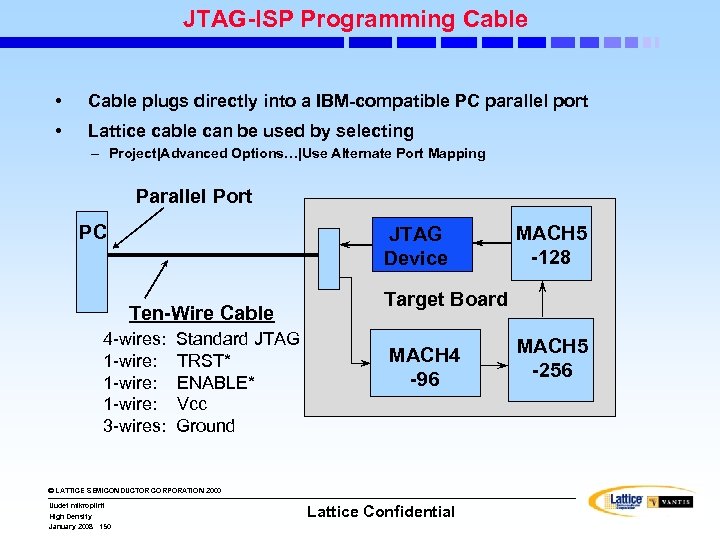 JTAG-ISP Programming Cable • Cable plugs directly into a IBM-compatible PC parallel port • Lattice cable can be used by selecting – Project|Advanced Options…|Use Alternate Port Mapping Parallel Port PC JTAG Device Ten-Wire Cable 4 -wires: 1 -wire: 3 -wires: Standard JTAG TRST* ENABLE* Vcc Ground Target Board MACH 4 -96 © LATTICE SEMICONDUCTOR CORPORATION 2000 Uudet mikropiirit High Density January 2008 150 MACH 5 -128 Lattice Confidential MACH 5 -256
 In-System Programming Procedure • Use Design. Direct software to create a JEDEC (fusemap) file • Load Vantis. PRO software onto the PC – With Design. Direct, Vantis. PRO is already loaded by default • Create a Chain file describing the JTAG chain – List devices in order from TDI to TDO – Specify “program” or “bypass” for each device – The Chain file may consist of a single device • Vantis. PRO does the rest! © LATTICE SEMICONDUCTOR CORPORATION 2000 Uudet mikropiirit High Density January 2008 151 Lattice Confidential
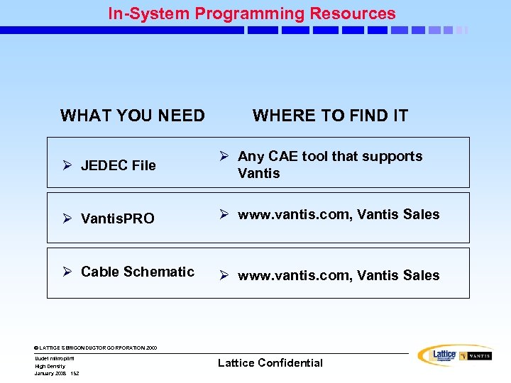 In-System Programming Resources WHAT YOU NEED WHERE TO FIND IT Ø JEDEC File Ø Any CAE tool that supports Vantis Ø Vantis. PRO Ø www. vantis. com, Vantis Sales Ø Cable Schematic Ø www. vantis. com, Vantis Sales © LATTICE SEMICONDUCTOR CORPORATION 2000 Uudet mikropiirit High Density January 2008 152 Lattice Confidential
 Concurrent Programming of Multiple Devices • Vantis. PRO can program many devices at once • Programming “wait” time is shared between all devices • Verification is performed serially • Concurrent programming further reduces costs of programming © LATTICE SEMICONDUCTOR CORPORATION 2000 Uudet mikropiirit High Density January 2008 153 Lattice Confidential
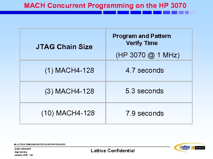 MACH Concurrent Programming on the HP 3070 JTAG Chain Size Program and Pattern Verify Time (HP 3070 @ 1 MHz) (1) MACH 4 -128 4. 7 seconds (3) MACH 4 -128 5. 3 seconds (10) MACH 4 -128 7. 9 seconds © LATTICE SEMICONDUCTOR CORPORATION 2000 Uudet mikropiirit High Density January 2008 154 Lattice Confidential
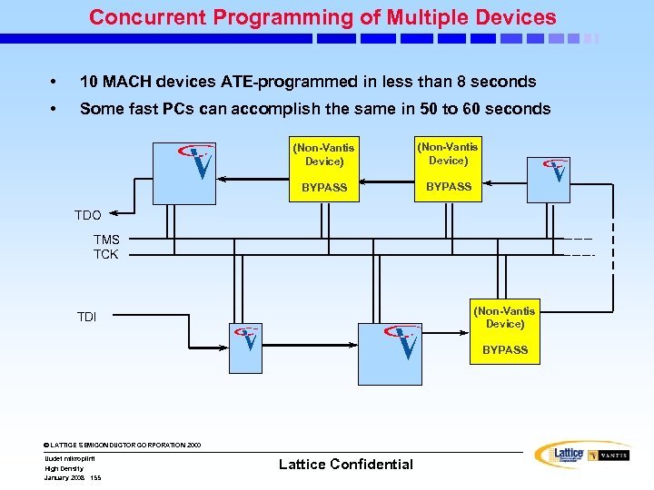 Concurrent Programming of Multiple Devices • 10 MACH devices ATE-programmed in less than 8 seconds • Some fast PCs can accomplish the same in 50 to 60 seconds (Non-Vantis Device) BYPASS TDO TMS TCK (Non-Vantis Device) TDI BYPASS © LATTICE SEMICONDUCTOR CORPORATION 2000 Uudet mikropiirit High Density January 2008 155 Lattice Confidential
 MACH Starter Kit • MACH Starter Kit includes: – – Software - CD ROM with Design. Direct Base software and Vantis. PRO Programming cable - Six-foot long and buffered MACH ISP demo board with M 4 -32/32 -7 JC & M 4 -64/32 -7 JC sample devices MACH ISP manual • Vantis. PRO software and cable schematic information available at: – Web site: www. vantis. com © LATTICE SEMICONDUCTOR CORPORATION 2000 Uudet mikropiirit High Density January 2008 156 Lattice Confidential
 Literature and Support • www. vantis. com/literature has all data sheets and application notes available. There always additional in development. • techsupport@vantis. com can answer all questions regarding MACH devices and software. • Technical call center: (888)VANTIS-1 • Reference design program for IP needs – SDRAM Controller – PCI Target – Page-mode DRAM Controller © LATTICE SEMICONDUCTOR CORPORATION 2000 Uudet mikropiirit High Density January 2008 157 Lattice Confidential


