db0175f96f3fa1d93a378c0683da2a8b.ppt
- Количество слайдов: 23
 HCAL Trigger Readout Technical Status and Progress Report D. Baden, T. Grassi http: //www. physics. umd. edu/hep/bu_oct_2002. pdf Boston University October 31, 2002 1
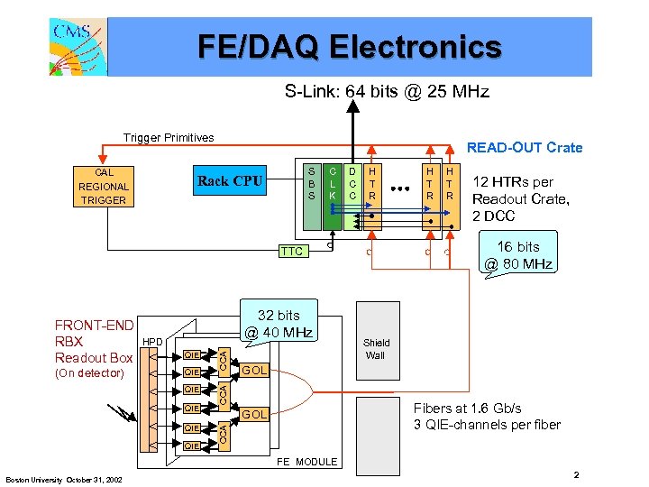 FE/DAQ Electronics S-Link: 64 bits @ 25 MHz Trigger Primitives CAL REGIONAL TRIGGER READ-OUT Crate S B S Rack CPU C L K D C C H T R QIE QIE QIE 12 HTRs per Readout Crate, 2 DCC Shield Wall GOL CCA QIE CCA HPD Fibers at 1. 6 Gb/s 3 QIE-channels per fiber GOL CCA (On detector) 32 bits @ 40 MHz H T R 16 bits @ 80 MHz TTC FRONT-END RBX Readout Box H T R FE MODULE Boston University October 31, 2002 2
 Trigger Readout Principal Functions 1. Receive front-end data for physics running • Synchronize optical links • Data validation and linearization • Extract Level 1 trigger info, transmit to Level 1 at 40 MHz • Pipeline data, wait for Level 1 accept • Upon receiving L 1 A: • Zero suppress, format, and transmit to the concentrator • NB: DAQ-Data in QIE-format (non-linear) no filter necessary anyway 2. Calibration processing and buffering of: • Radioactive source calibration data • Laser/LED calibration data 3. Support a VME data spy monitoring Boston University October 31, 2002 3
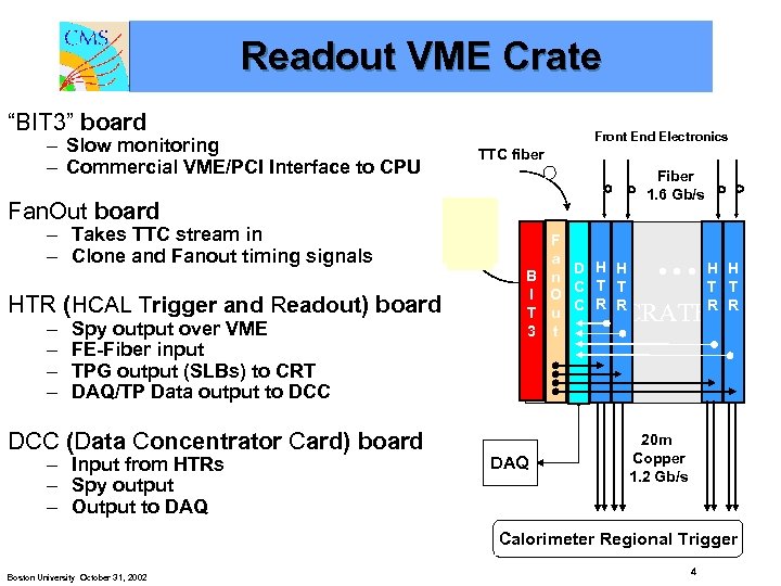 Readout VME Crate “BIT 3” board – Slow monitoring – Commercial VME/PCI Interface to CPU Front End Electronics TTC fiber Fiber 1. 6 Gb/s Fan. Out board – Takes TTC stream in – Clone and Fanout timing signals HTR (HCAL Trigger and Readout) board D – C C– Spy output over VME FE-Fiber input – TPG output (SLBs) to CRT – DAQ/TP Data output to DCC (Data Concentrator Card) board – Input from HTRs – Spy output – Output to DAQ F a H H B n D T T I O C R R T u C 3 t . . . H H T T R R VME CRATE DAQ 20 m Copper 1. 2 Gb/s Calorimeter Regional Trigger Boston University October 31, 2002 4
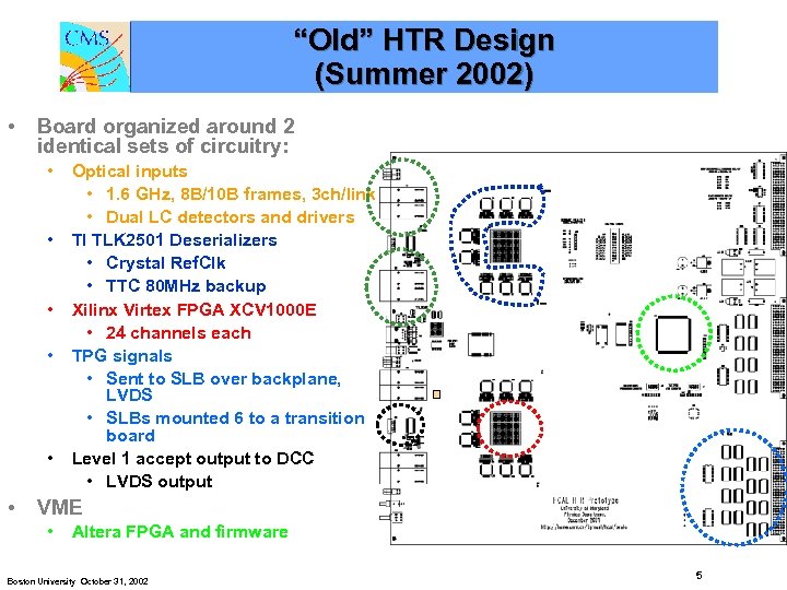 “Old” HTR Design (Summer 2002) • Board organized around 2 identical sets of circuitry: • • • Optical inputs • 1. 6 GHz, 8 B/10 B frames, 3 ch/link • Dual LC detectors and drivers TI TLK 2501 Deserializers • Crystal Ref. Clk • TTC 80 MHz backup Xilinx Virtex FPGA XCV 1000 E • 24 channels each TPG signals • Sent to SLB over backplane, LVDS • SLBs mounted 6 to a transition board Level 1 accept output to DCC • LVDS output OLD DESIGN VME • Altera FPGA and firmware Boston University October 31, 2002 5
 HTR Functional Experience • What was tested: • VME fully tested and working • Some changes necessary to conform to CMS VME standards • Optical links and synchronization • No indication of any problems. Big success here – was a real worry • LVDS to DCC • Tested, working (Will change cable/connector to Cat 6/RJ 45) • Fanout of timing signals on two Cat 5 cables • Plan to change to a single Cat 6 or Cat 7 cable (very low cross-talk) • Firmware – full tests of: • Pipeline and L 1 A triggering capability • In-line histogramming for source calibration • TTCrx • Not working at all (4 bad on 4 tested). • What was not tested: Anything to do with TPG Boston University October 31, 2002 6
 HTR Board Experience • Produced ~12 boards • Several bare boards were delivered warped • Many opens under FPGA after assembly (~9 boards) • Some fixed after reflow (a few) • Some worse after reflow (shorts) • X-rayed a few boards, sometimes inconclusive • Some opens on VME side • Non BGA FPGA, indicates bad vias • Few other various open circuits • Finally got ~8 boards to “work” • Questionable reliability Boston University October 31, 2002 7
 Resulting Modifications • Change board from using white-tin to gold traces • This process was sold to us by the board maker. Our mistake. • Used only for very high volume, cost competitive products, very difficult and expensive to control. • Gold is flatter and not very much more expensive (~$50/board), better for FPGAs • Change assembly house • Insufficient Quality Control on current assembler – they are fired. • We visited 2 high-end assemblers • Modern Machines • Step up and step down oven temp control. • In-line X-ray for BGA QC • Manufacturability Review • Add stiffeners to HTRS • Flexability of 9 U VME boards was underestimated • Worry: fine-line BGA (FBGA) can pop connections • Change from FBGA (1. 0 mm pitch) to BGA (1. 27 mm pitch) • No additional expense, plenty of available real estate, no need to push • Full JTAG capabilities added • Will help with debugging • By making these changes… • We have profited from the summer • We have reduced our production risk considerably Boston University October 31, 2002 8
 HTR Design Changes • SLB transition board issues: • Worries about so many LVDS signals over backplane for old design • Routing is too complicated • Many signals going to same backplane location • Requires multi-layer routing with many vias • TPG cables very thick • Mechanical issues are very worrisome • SLB changes needed (e. g. height reduced after ECAL redesign…) • Solution: move SLB’s to HTR motherboard • Benefits: • Mechanically attach SLB’s to HTR front panel for mechanical stability • Eases routing requirements, reduces board and assembly risks, cheaper too • Change from Xilinx Virtex. E to Virtex 2 • More resources, block ram, hardware multipliers • Big cost reduction (save $300 k) • More modern chip for long-term maintenance • Clock synchronization • Decouple “ 80 MHz” crystal from FPGA system clock • Will allow us to use crystal to maintain synchronization of serdes • This gives us 2 solutions for our “ 40 ps” jitter requirement issue Boston University October 31, 2002 9
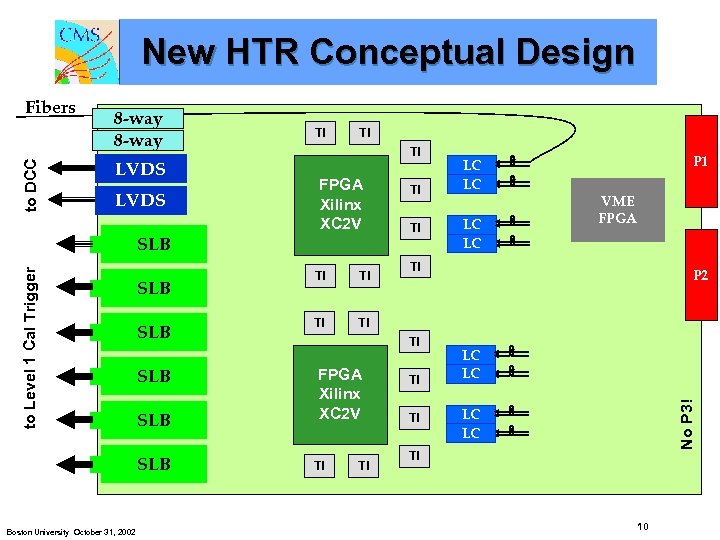 New HTR Conceptual Design 8 -way LVDS TI TI TI FPGA Xilinx XC 2 V to Level 1 Cal Trigger SLB SLB SLB Boston University October 31, 2002 TI TI TI P 1 LC LC VME FPGA TI P 2 TI TI FPGA Xilinx XC 2 V TI TI LC LC No P 3! to DCC Fibers LC LC TI 10
 HTR Cost Issues • Optical parts • LC receivers quote went up from $80 to $140 • $640/HTR board, $155 k total goes up to $270 k • We just learned this. Rob is working on them. • Would probably be cost effective now to go with mass terminated receivers (PAROLI) • But would involve board layout changes, will effect schedule, est ~2 months • FPGA • Virtex 2 2000 ($472 each, $944/board) current choice ($300 k savings), but… • HCAL sections where there is no summing means more LUTs, more resources. • XC 2 V 2000 is just only large enough • VIrtex 2 3000 ($743 each, $1486/board) works, pin compatible • Cost increase is $130 k total. • Can be minimized by only building HTRs with 3000 part for those sections of HCAL where there is no summing • Reduces cost increase to ~$30 k if only HB has the larger chips • Obvious down side is that we would have 2 types of HTRs • Means that HB cards can be used anywhere but not vice versa Boston University October 31, 2002 11
 HTR Cost Issues (cont) • SLB cost increases • Previous costs were ~$100/SLB • We need 575 total, or $60 k in previous budgets • Current estimates from Dasilva: • 292 CHF parts, 100 CHF assembly/testing = $250/SLB • New estimates mean increase to $144 k ($86 k increase) • We are investigating whether we can buy the parts and assemble them here • SLB transition card • Abandoned (see above) • Cost savings of $66 k • TPG cables • Wesley private communication cost estimate was ~$100/cable (2 yrs ago) • Current estimate: $200/cable, $150/connectors and assembly • Increases our cost from $52 k to $182 k • We are going to have to do our own cost estimates. • Dasilva is testing a much cheaper cable • It is important to push Wesley to decrease the spec from 20 m to 10 m • Can use smaller cable, saves money, and saves us 2 clock ticks in L 1 latency Boston University October 31, 2002 12
 Cost/Maintenance Issues • Currently, we have 10% spares in the budget. • Optical parts will surely be difficult to get in >3 years • Failure rate is expected to be low but… • If we need more…we propose we buy an extra 10% spares • Additional $15 k • FPGAs will probably be ok for 5 years but will be more and more difficult to get, and more expensive. • TI serdes will probably be difficult to replace. • $200/HTR board, $46 k total • We should buy an extra 10% of these and let them sit in a drawer • PCBs • We propose to build 20% spare PCBs but only stuff 10% • Gives us some breathing room in case of future disasters. Boston University October 31, 2002 13
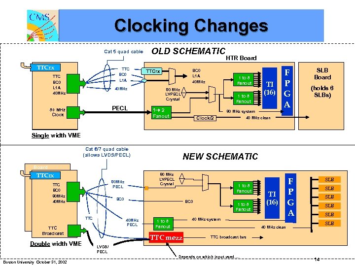 Clocking Changes Cat 5 quad cable OLD SCHEMATIC TTC Fanout Board TTCrx TTC BC 0 L 1 A 40 MHz PECL 80 MHz Clock BC 0 L 1 A 40 MHz TTCrx HTR Board 1 to 8 Fanout 80 MHz LVPECL Crystal 1 to 8 Fanout 1 2 Fanout TI (16) 80 MHz system Clock/2 F P G A SLB Board (holds 6 SLBs) 40 MHz clean Single width VME Cat 6/7 quad cable (allows LVDS/PECL) NEW SCHEMATIC TTC Fanout Board TTCrx 80 MHz PECL TTC BC 0 80 MHz 40 MHz 1 to 8 Fanout BC 0 TTC BC 0 40 MHz PECL TTC Broadcast Double width VME 80 MHz LVPECL Crystal 1 to 8 Fanout 40 MHz system 1 to 8 Fanout SLB SLB SLB 40 MHz clean TTC mezz TTC broadcast bus LVDS/ PECL Depends on which input used…. Boston University October 31, 2002 TI (16) F P G A 14
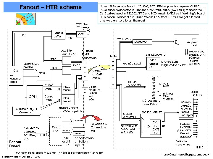 Fanout – HTR scheme Notes: SLBs require fanout of CLK 40, BC 0. FE-link possibly requires CLK 80. PECL fanout was tested in TB 2002. One Cat 6 E cable (low x-talk) replaces the 2 Cat 5 cables used in TB 2002. TTC and BC 0 remain LVDS as in Weiming’s board. HTR needs Broadcast bus, BCnt. Res and L 1 A: from TTCrx if we get it to work, otherwise we have to fan them out. TTC fiber Fanout buffer TTC O/E TTC LVDS Low-jitter Fanout x 15 TTC Brdcst<7: 2>, Brcst. Str TTCrx ~Fifteen RJ 45 connectors LVDS BC 0 FPGA (or daughter card) CLK 40 LVDS QPLL PECL fanout CLK 80 LVDS AN 1568/D Fig 11 Onsemi. com . . . PECL fanout Cat 6 E or Cat 7 cable 2 Test Points for CLK 40 and BC 0 NB 100 LVEP 221 is LVDS compatible Fanout Board Brdcst<7: 2>, Brcst. Str, CMOS BCnt. Res, L 1 A ……. . LVDS or diff PECL 15 Cables & Connectors tbd 15 connectors on bottom layer ? 9 U Front-panel space = 325 mm ; => space per connector ~ 21. 5 mm Boston University October 31, 2002 RX_BC 0 LVDS . . . LVDS Fanout x 8 Diff. to 6 SLBs Single-end to 2 xilinx Q 1 Q 2 CLK 40 Q 3 3. 3 V-PECL Q 4 Q 5 Q 6 Q 7 Q 8 MC 100 LVE 310 3. 3 V PECL CLK 80 3. 3 V-PECL ……. . Fanout x 15 e. g. DS 90 LV 110 RJ 45 . . TTC daughter card IN IN_b DS 90 LV 001 80. 0789 MHz 3. 3 V crystal Diff. PECL MC 100 LVEL 37 CK CK CK/2 Brdcst<7: 2>, Brcst. Str, L 1 A, BCnt. Res to xilinx and SLBs To 6 SLBs 8 clks to TLKs Diff. to 2 Xilinx + termin. PCK 953 LVPECLto-LVTTL Fanout (top layer) 8 clks to TLKs + TPs HTR Tullio Grassi
 HCAL Tri. DAS Integration • First integration completed, summer 02 • FE HTR DCC SLINK CPU • All links well established • No obvious clocking problems • Work needed on synch monitoring and reporting • Improvements expected using crystal for TI refclk • Will always have TTC/QPLL clock as backup… • HTR firmware fairly mature • Switch to Virtex 2 all but complete • TPG and BCID ready but not tested • To commence when next HTR version delivered and Wisconsin TPG boards delivered (est Q 4 2002) • Will be main effort when next HTR version arrives Dec 2002 Boston University October 31, 2002 16
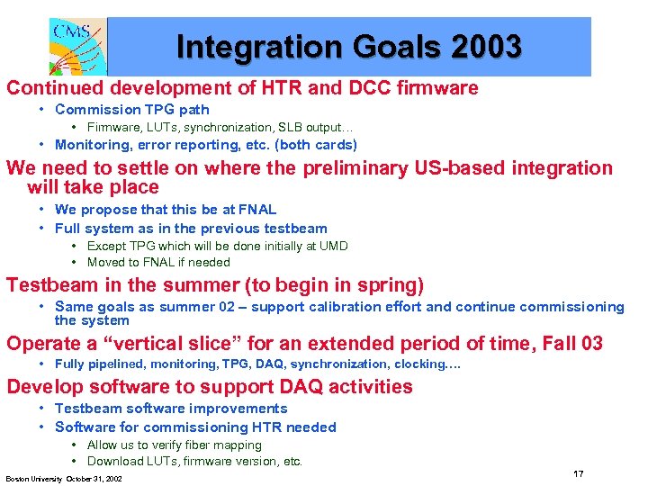 Integration Goals 2003 Continued development of HTR and DCC firmware • Commission TPG path • Firmware, LUTs, synchronization, SLB output… • Monitoring, error reporting, etc. (both cards) We need to settle on where the preliminary US-based integration will take place • We propose that this be at FNAL • Full system as in the previous testbeam • Except TPG which will be done initially at UMD • Moved to FNAL if needed Testbeam in the summer (to begin in spring) • Same goals as summer 02 – support calibration effort and continue commissioning the system Operate a “vertical slice” for an extended period of time, Fall 03 • Fully pipelined, monitoring, TPG, DAQ, synchronization, clocking…. Develop software to support DAQ activities • Testbeam software improvements • Software for commissioning HTR needed • Allow us to verify fiber mapping • Download LUTs, firmware version, etc. Boston University October 31, 2002 17
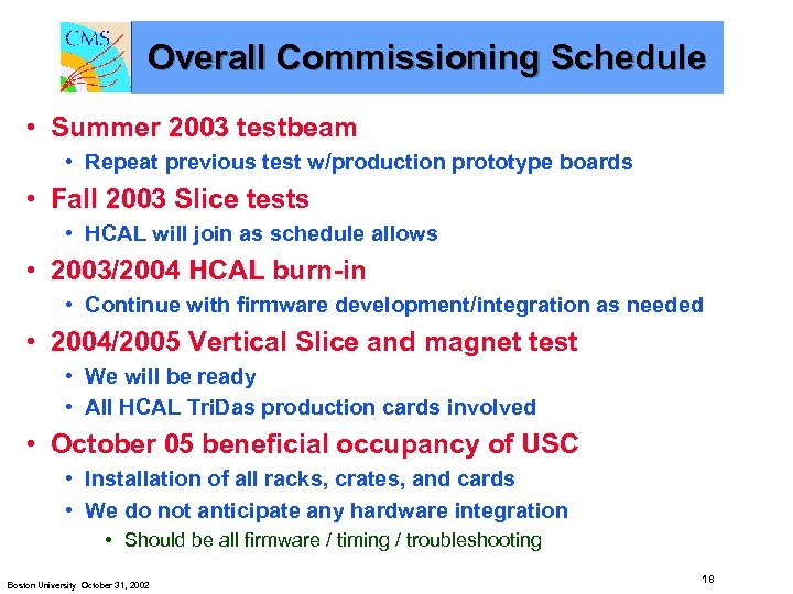 Overall Commissioning Schedule • Summer 2003 testbeam • Repeat previous test w/production prototype boards • Fall 2003 Slice tests • HCAL will join as schedule allows • 2003/2004 HCAL burn-in • Continue with firmware development/integration as needed • 2004/2005 Vertical Slice and magnet test • We will be ready • All HCAL Tri. Das production cards involved • October 05 beneficial occupancy of USC • Installation of all racks, crates, and cards • We do not anticipate any hardware integration • Should be all firmware / timing / troubleshooting Boston University October 31, 2002 18
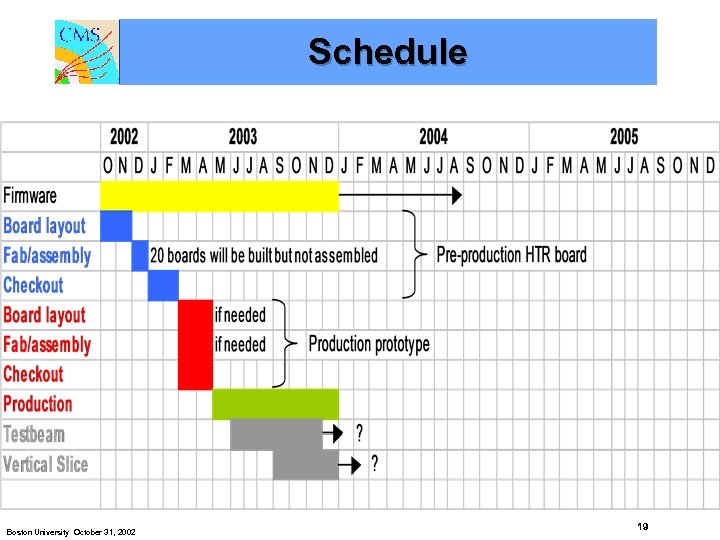 Schedule Boston University October 31, 2002 19
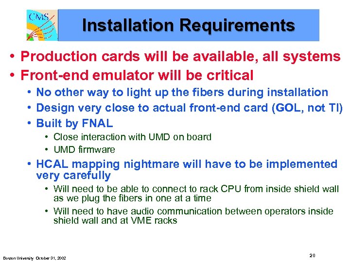 Installation Requirements • Production cards will be available, all systems • Front-end emulator will be critical • No other way to light up the fibers during installation • Design very close to actual front-end card (GOL, not TI) • Built by FNAL • Close interaction with UMD on board • UMD firmware • HCAL mapping nightmare will have to be implemented very carefully • Will need to be able to connect to rack CPU from inside shield wall as we plug the fibers in one at a time • Will need to have audio communication between operators inside shield wall and at VME racks Boston University October 31, 2002 20
 Installation Manpower Needs • Drawing on D Level 2 experience for the current Tevatron Run 2 a… • Each significant card requires on-site expertise: • Probably 1 -2 postdoc-level (or above) and 1 engineer • Maybe the same engineer for both DCC and HTR… • HCAL will have an electronics setup at CERN • Total personnel estimate: • • Front End 1 HTR 2 DCC 2 Miscellaneous (grad students, transients, etc. ) maybe 4? • Very difficult to say with any accuracy Boston University October 31, 2002 21
 HTR Board Maintenance • HTR boards will all be at CERN in ~12 months • Repairs can come back to UMD on as needed basis • But not if there is a disaster in 3 or more years – unknown staffing… • Dick Kellogg will be at CERN. (forever maybe) • Therefore…HCAL electronics guy at CERN should be knowledgeable on HTR details. • All relevant design files should be placed into archival storage (EDMS, CVS, whatever…) • PDF schematics • Design tool files • Unfortunately we don’t use Cadence…. but most assemblers can understand most varieties • Gerber files (specifies PCB artwork) Boston University October 31, 2002 22
 HTR Firmware Maintenance • CMS runs in 2008… • Not many HEP experiments have had sufficient experience to guide us… • We propose the following: • 1 or 2 computers/laptops should be purchased and fitted with the relevant tools: • Xilinx and Altera tools with specified versions to compile source code • Different versions WILL produce different timing in the results • Synplicity etc. synthesis tools are not used but should be included just in case… • Aldec simulator needed for verification of timing after changes • All of these should be node locked (e. g. not run off of license servers) • All firmware versions for ANY HCAL FPGA: • Should have a VME readable version number • Should be archived (CVS or whatever CERN supports) • Firmware maintenance will be a combination of: • UMD personnel • CERN HCAL electronics guru • Other universities which join CMS looking for responsibility Boston University October 31, 2002 23


