 H 8 Peek (H 8 S, H 8 SX, 300 H Tiny, SLP) February 2005 December, 2004
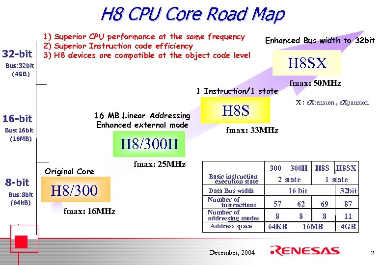 H 8 CPU Core Road Map 32 -bit 1) Superior CPU performance at the same frequency 2) Superior Instruction code efficiency 3) H 8 devices are compatible at the object code level Enhanced Bus width to 32 bit H 8 SX Bus: 32 bit (4 GB) 1 Instruction/1 state 16 MB Linear Addressing Enhanced external mode 16 -bit Bus: 16 bit (16 MB) 8 -bit Bus: 8 bit (64 k. B) fmax: 50 MHz X : e. Xtension , e. Xpansion H 8 S fmax: 33 MHz H 8/300 H Original Core H 8/300 fmax: 16 MHz fmax: 25 MHz Basic instruction execution state Data Bus width Number of instructions Number of addressing modes Address space December, 2004 300 H H 8 SX 2 state 1 state 8 bit 16 bit 32 bit 57 8 64 KB 62 69 8 8 16 MB 87 11 4 GB 2
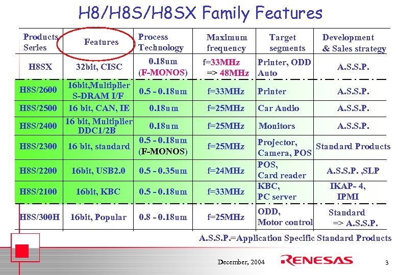 H 8/H 8 SX Family Features Products Series Features H 8 SX 32 bit, CISC Process Technology 0. 18 um (F-MONOS) 16 bit, Multiplier 0. 5 - 0. 18 um S-DRAM I/F H 8 S/2500 16 bit, CAN, IE 0. 18 um H 8 S/2400 16 bit, Multiplier 0. 18 um DDC 1/2 B 0. 5 - 0. 18 um H 8 S/2300 16 bit, standard (F-MONOS) H 8 S/2600 Maximum frequency Target segments f=33 MHz Printer, ODD => 48 MHz Auto Development & Sales strategy A. S. S. P. f=33 MHz Printer A. S. S. P. f=25 MHz Car Audio A. S. S. P. f=25 MHz Monitors A. S. S. P. f=25 MHz Projector, Standard Products Camera, POS, A. S. S. P. , SLP Card reader KBC, IKAP- 4, PC server IPMI H 8 S/2200 16 bit, USB 2. 0 0. 5 - 0. 35 um f=24 MHz H 8 S/2100 16 bit, KBC 0. 5 - 0. 18 um f=33 MHz H 8 S/300 H 16 bit, Popular 0. 8 - 0. 18 um f=25 MHz ODD, Motor control Standard => A. S. S. P. =Application Specific Standard Products December, 2004 3
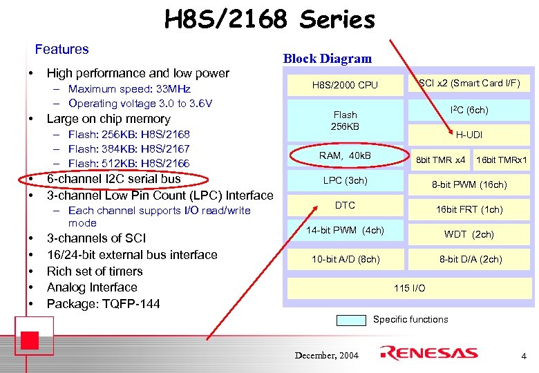 H 8 S/2168 Series Features • High performance and low power – Maximum speed: 33 MHz – Operating voltage 3. 0 to 3. 6 V • Large on chip memory – Flash: 256 KB: H 8 S/2168 – Flash: 384 KB: H 8 S/2167 – Flash: 512 KB: H 8 S/2166 • • 6 -channel I 2 C serial bus 3 -channel Low Pin Count (LPC) Interface – Each channel supports I/O read/write mode • • • Block Diagram 3 -channels of SCI 16/24 -bit external bus interface Rich set of timers Analog Interface Package: TQFP-144 H 8 S/2000 CPU SCI x 2 (Smart Card I/F) Flash 256 KB I 2 C (6 ch) H-UDI RAM, 40 k. B 8 bit TMR x 4 16 bit TMRx 1 LPC (3 ch) 8 -bit PWM (16 ch) DTC 16 bit FRT (1 ch) 14 -bit PWM (4 ch) WDT (2 ch) 10 -bit A/D (8 ch) 8 -bit D/A (2 ch) 115 I/O Specific functions December, 2004 4
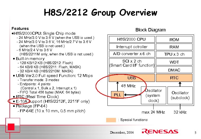 H 8 S/2212 Group Overview Features H 8 S/2000 CPU: Single Chip mode - 24 MHz/3. 0 V to 3. 6 V (when the USB is used. ) - 24 MHz/3. 0 V to 3. 6 V, 16 MHz/2. 7 V to 3. 6 V (when the USB is not used. ) - 6 MHz/2. 4 V to 3. 6 V (H 8 S/2211 M only, when the USB is not used. ) Built-in memory - 128 KB/12 KB (H 8 S/2212: Flash) - 64 KB/8 KB (H 8 S/2211: Flash, MASK) - 32 KB/4 KB (H 8 S/2210 M: MASK) Block Diagram H 8 S/2000 CPU ROM Interrupt cotroller RAM A/D converter x 6 ch TPU x 3 ch SCI x 2 ch (Smart Card I/F function) WDT DMAC USB Ver 2. 0 Full speed Function: 12 Mbps - Transfer mode: 3 modes - Endpoints: 4 points (Control x 1, Bulk x 2, Interrupt x 1) - FIFO Total 456 bytes (MAX: 64 bytes) RTC (Real Time Clock) E-10 A support (H 8 S/2212 F, 2211 F only) Package (FP-64) - FP-64 E (10 x 10 mm, 0. 5 mm pitch) USB RTC 48 MHz Oscillator (subclock) max 24 MHz PLL Oscillator (system clock) 32 k. Hz : Special functions December, 2004 5
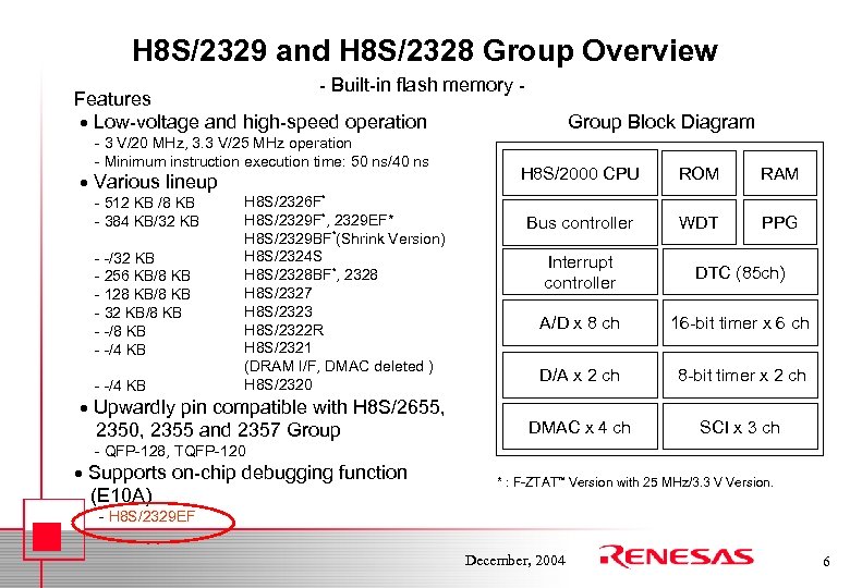 H 8 S/2329 and H 8 S/2328 Group Overview - Built-in flash memory - Features Low-voltage and high-speed operation - 3 V/20 MHz, 3. 3 V/25 MHz operation - Minimum instruction execution time: 50 ns/40 ns Various lineup - 512 KB /8 KB - 384 KB/32 KB - -/32 KB - 256 KB/8 KB - 128 KB/8 KB - 32 KB/8 KB - -/4 KB H 8 S/2326 F* H 8 S/2329 F*, 2329 EF* H 8 S/2329 BF*(Shrink Version) H 8 S/2324 S H 8 S/2328 BF*, 2328 H 8 S/2327 H 8 S/2323 H 8 S/2322 R H 8 S/2321 (DRAM I/F, DMAC deleted ) H 8 S/2320 Upwardly pin compatible with H 8 S/2655, 2350, 2355 and 2357 Group Block Diagram H 8 S/2000 CPU ROM RAM Bus controller WDT PPG Interrupt controller DTC (85 ch) A/D x 8 ch 16 -bit timer x 6 ch D/A x 2 ch 8 -bit timer x 2 ch DMAC x 4 ch SCI x 3 ch - QFP-128, TQFP-120 Supports on-chip debugging function (E 10 A) * : F-ZTAT Version with 25 MHz/3. 3 V Version. - H 8 S/2329 EF December, 2004 6
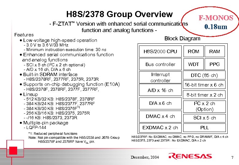 H 8 S/2378 Group Overview - F-ZTAT F-MONOS 0. 18 um Version with enhanced serial communications function and analog functions Features Block Diagram Low-voltage high-speed operation - 3. 0 V to 3. 6 V/33 MHz - Minimum instruction execution time: 30 ns Enhanced serial communications function and analog functions - SCI x 5 ch (I 2 C x 2 ch optional) - A/D x 16 ch, D/A x 6 ch Built-in SDRAM interface - H 8 S/2378 RF, 2377 RF, 2375 R, 2373 R Supports on-chip debugging function (E 10 A) - H 8 S/2378 F, 2378 RF, 2377 RF, Lineup - 512 KB/32 KB: H 8 S/2378 F, 2378 RF - 384 KB/24 KB: H 8 S/2377 F, 2377 RF - 384 KB/30 KB: H 8 S/2376 F*1 - 256 KB/16 KB: H 8 S/2375, 2375 R - -/16 KB: H 8 S/2373, 2373 R Multiple-pin package - LQFP-144 *1: Reduced peripheral functions Note: Not pin-compatible with the H 8 S/2338 and 2678 Group H 8 S/2378 F and 2378 RF have VCL pin. H 8 S/2000 CPU ROM RAM Bus controller WDT PPG Interrupt controller A/D x 16 ch DTC (85 ch) 16 -bit timer x 6 ch 8 -bit timer x 2 ch D/A x 6 ch I 2 C x 2 ch (Option) DMAC x 4 ch SCI x 5 ch EXDMAC x 2 ch PLL H 8 S/2376 F: No EXDMAC, no PPG, no DRAMI/F, D/A x 4 ch H 8 S/2375, 2373 and 2373 R : No EXDMAC, D/A x 2 ch December, 2004 7
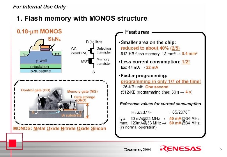
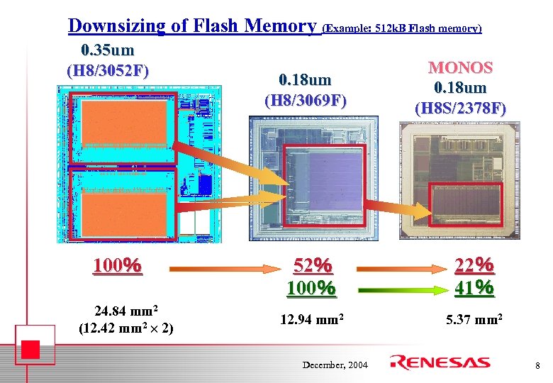 Downsizing of Flash Memory (Example: 512 k. B Flash memory) 0. 35 um (H 8/3052 F) 100% 24. 84 mm 2 (12. 42 mm 2 2) 0. 18 um (H 8/3069 F) MONOS 0. 18 um (H 8 S/2378 F) 52% 100% 22% 41% 12. 94 mm 2 5. 37 mm 2 December, 2004 8
 December, 2004 9
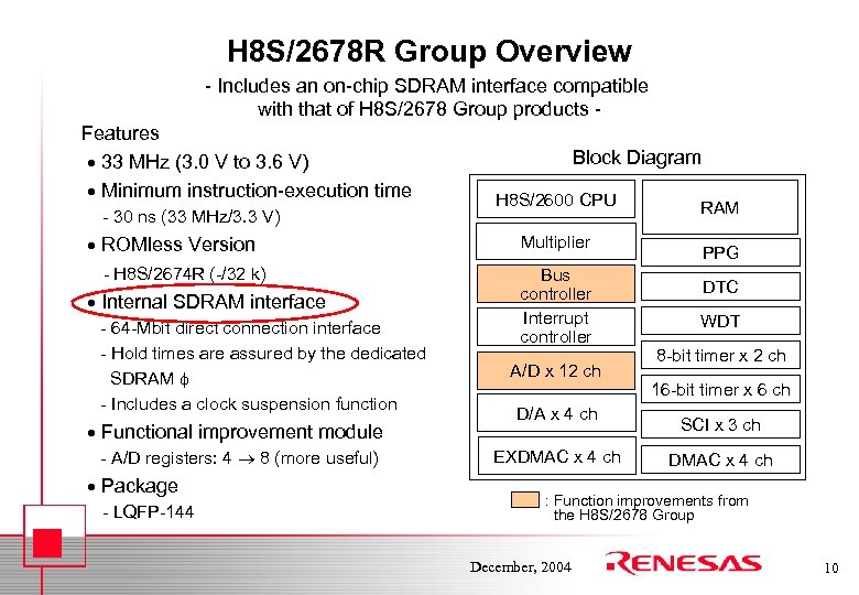 H 8 S/2678 R Group Overview - Includes an on-chip SDRAM interface compatible with that of H 8 S/2678 Group products Features 33 MHz (3. 0 V to 3. 6 V) Minimum instruction-execution time - 30 ns (33 MHz/3. 3 V) ROMless Version - H 8 S/2674 R (-/32 k) Internal SDRAM interface - 64 -Mbit direct connection interface - Hold times are assured by the dedicated SDRAM - Includes a clock suspension function Functional improvement module - A/D registers: 4 8 (more useful) Package - LQFP-144 Block Diagram H 8 S/2600 CPU Multiplier Bus controller Interrupt controller A/D x 12 ch D/A x 4 ch EXDMAC x 4 ch RAM PPG DTC WDT 8 -bit timer x 2 ch 16 -bit timer x 6 ch SCI x 3 ch DMAC x 4 ch : Function improvements from the H 8 S/2678 Group December, 2004 10
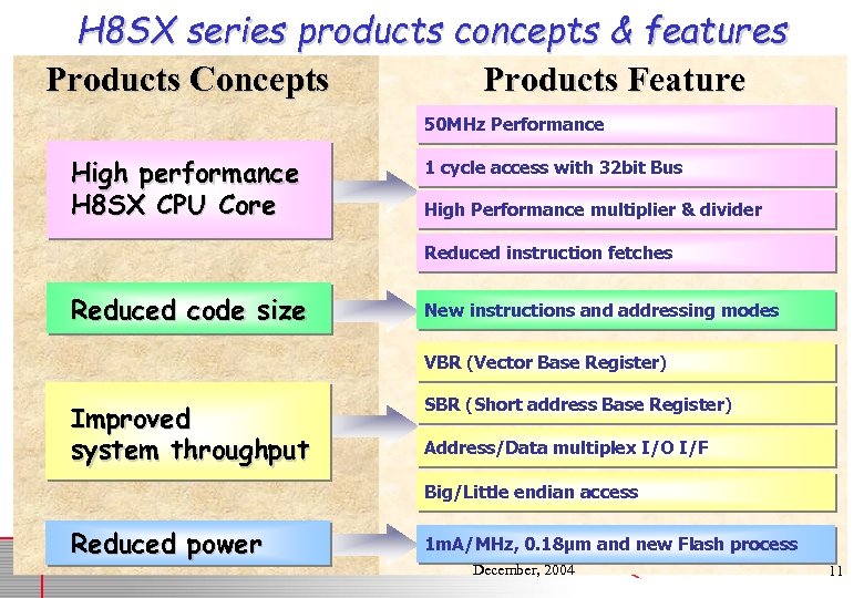 H 8 SX series products concepts & features Products Concepts Products Feature 50 MHz Performance High performance H 8 SX CPU Core 1 cycle access with 32 bit Bus High Performance multiplier & divider Reduced instruction fetches Reduced code size New instructions and addressing modes VBR (Vector Base Register) Improved system throughput SBR (Short address Base Register) Address/Data multiplex I/O I/F Big/Little endian access Reduced power 1 m. A/MHz, 0. 18μm and new Flash process December, 2004 11
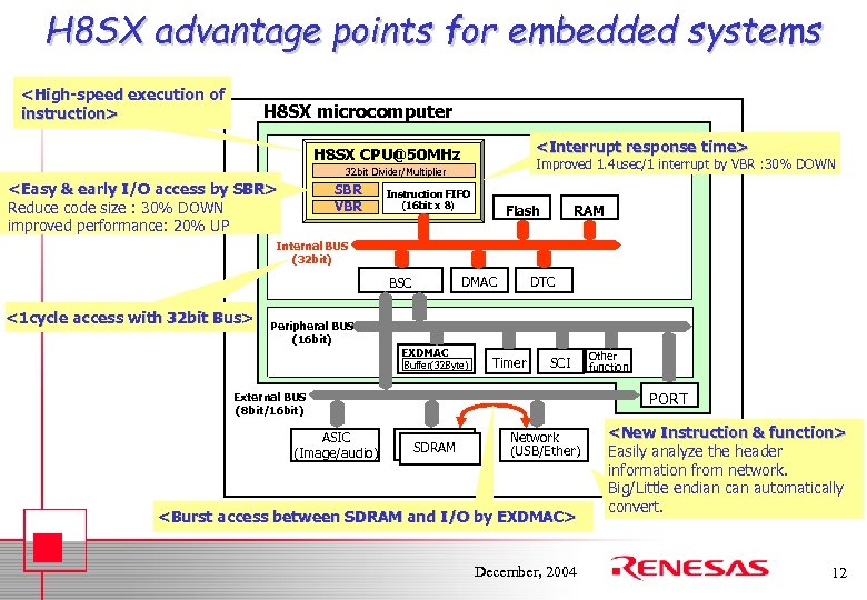 H 8 SX advantage points for embedded systems
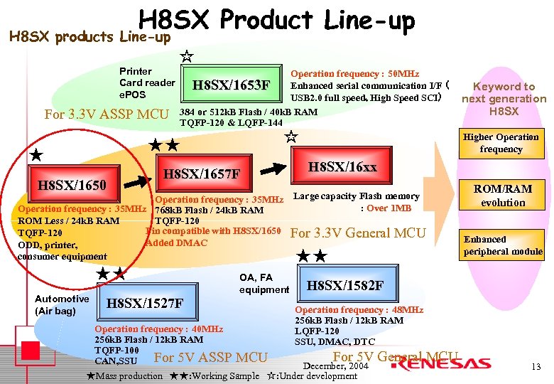 H 8 SX Product Line-up H 8 SX products Line-up ☆ Printer Card reader e. POS For 3. 3 V ASSP MCU Operation frequency : 50 MHz H 8 SX/1653 F Enhanced serial communication I/F ( USB 2. 0 full speed、High Speed SCI) 384 or 512 k. B Flash / 40 k. B RAM TQFP-120 & LQFP-144 ☆ ★★ ★ H 8 SX/1650 H 8 SX/1657 F Operation frequency : 35 MHz 768 k. B Flash / 24 k. B RAM ROM Less / 24 k. B RAM TQFP-120 Pin compatible with H 8 SX/1650 TQFP-120 Added DMAC ODD, printer, consumer equipment ★★ Automotive (Air bag) H 8 SX/1527 F OA, FA equipment Keyword to next generation H 8 SX Higher Operation frequency H 8 SX/16 xx Large capacity Flash memory : Over 1 MB For 3. 3 V General MCU ★★ ROM/RAM evolution Enhanced peripheral module H 8 SX/1582 F Operation frequency : 48 MHz 256 k. B Flash / 12 k. B RAM LQFP-120 SSU, DMAC, DTC Operation frequency : 40 MHz 256 k. B Flash / 12 k. B RAM TQFP-100 For 5 V ASSP MCU CAN, SSU December, 2004 ★Mass production ★★: Working Sample ☆: Under development General MCU 13
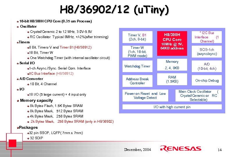 H 8/36902/12 (u. Tiny) 16 -bit H 8/300 H CPU Core (0. 35 um Process) Oscillator Crystal/Ceramic 2 to 12 MHz, 3. 0 V-5. 5 V RC Oscillator Typical 8 MHz, +/-2%(after trimming) Timers 8 Bit, Timers V and Timer B 1(H 8/36912) 16 Bit, Timer W One Watchdog Timer (with internal oscillator circuit) Serial I/O 1 -ch Async. /Sync. Serial Com. Interface IIC Bus Interface (H 8/36912) A/D Converter 10 Bit, 4 Channel I/O 18 I/O (5 large current) + 4 input only Memory capacity Timer V, B 1 (2 ch, 8 -bit) Timer W (1 ch, 16 -bit, PWM mode) H 8/300 H CPU Core 10 MHz @ 5 V, 64 KB address Memory * I 2 C Bus Interface (1 Channel) SCI 3 -1 ch (async/sync) Watchdog Timer 2, 4, 8 KB A/D (10 -bit, 4 ch) Address Break Controller RAM (1. 5 KB) On-chip Debug Power on Reset and Low Voltage Detect 8 k Bytes Flash, 1. 5 K Bytes SRAM 8 k Bytes Mask, 512 Bytes SRAM 4 k Bytes Mask, 256 Bytes SRAM 2 k Bytes Mask, 256 Bytes SRAM (only in H 8/36902) Main Clock Oscillator ( Crystal/Ceramic or RC Selectable) I/O with high current pin Packages 32 pin SSOP, LQFP( 7 mm x 7 mm) 32 SDIP December, 2004 14
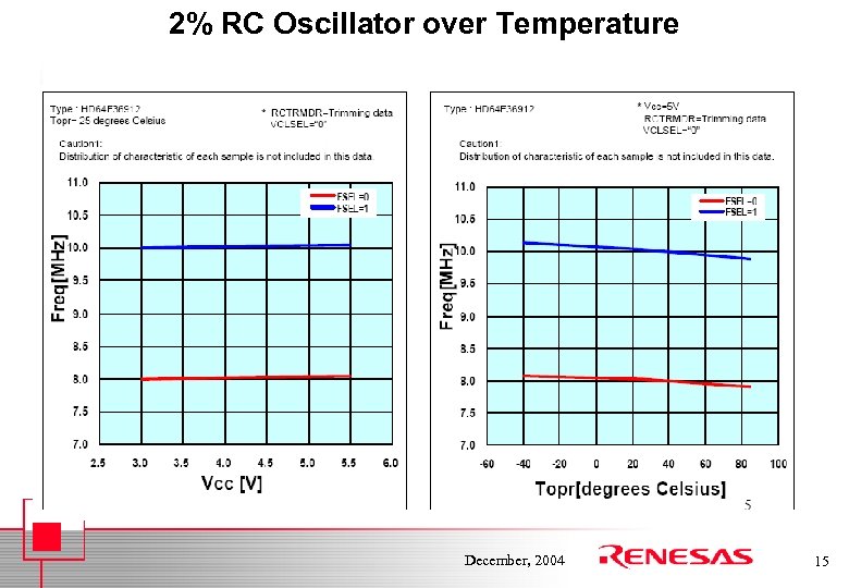 2% RC Oscillator over Temperature December, 2004 15
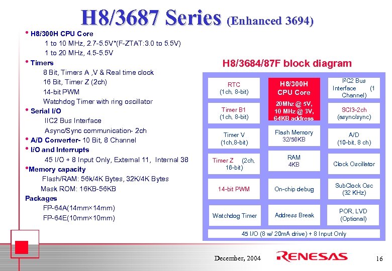 H 8/3687 Series (Enhanced 3694) • H 8/300 H CPU Core 1 to 10 MHz, 2. 7 -5. 5 V*(F-ZTAT: 3. 0 to 5. 5 V) 1 to 20 MHz, 4. 5 -5. 5 V • Timers 8 Bit, Timers A , V & Real time clock 16 Bit, Timer Z (2 ch) 14 -bit PWM Watchdog Timer with ring oscillator • Serial I/O IIC 2 Bus Interface Async/Sync communication- 2 ch • A/D Converter- 10 Bit, 8 Channel • I/O and Interrupts 45 I/O + 8 Input Only, External 11, Internal 38 • Memory capacity Flash/RAM: 56 k/4 K Bytes, 32 K/4 K Bytes Mask ROM: 16 KB-56 KB Packages FP-64 A(14 mm× 14 mm) FP-64 E(10 mm× 10 mm) H 8/3684/87 F block diagram RTC (1 ch, 8 -bit) H 8/300 H CPU Core I 2 C 2 Bus Interface (1 Channel) Timer B 1 (1 ch, 8 -bit) 20 Mhz @ 5 V, 10 MHz @ 3 V, 64 KB address SCI 3 -2 ch (async/sync) Timer V (1 ch, 8 -bit) Flash Memory 32/56 KB A/D (10 -bit, 8 ch) Timer Z (2 ch, 16 -bit) RAM 4 KB Clock Oscillator 14 -bit PWM On-chip debug Sub. Clock Osc (32 KHz) Watchdog Timer Address Break POR, LVD (Optional) 45 I/O (8 w/ 20 m. A drive) + 8 Input Only December, 2004 16
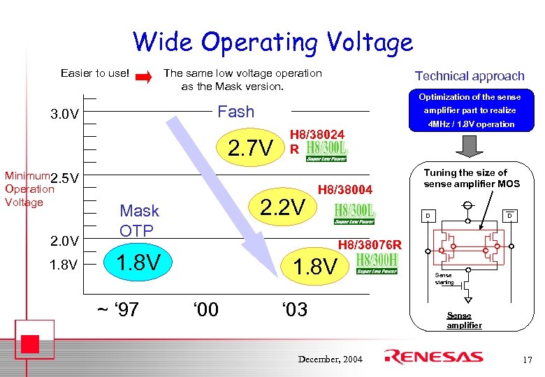 Wide Operating Voltage Easier to use! The same low voltage operation as the Mask version. amplifier part to realize 2. 7 V 2. 0 V 1. 8 V Optimization of the sense Fash 3. 0 V Minimum 2. 5 V Operation Voltage Technical approach 2. 2 V Mask OTP H 8/38004 Tuning the size of sense amplifier MOS D D H 8/38076 R 1. 8 V ~ ‘ 97 H 8/38024 R 4 MHz / 1. 8 V operation 1. 8 V ‘ 00 ‘ 03 December, 2004 Sense starting Sense amplifier 17
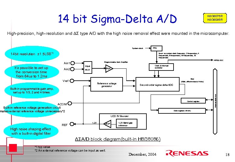 14 bit Sigma-Delta A/D H 8/38076 R H 8/38086 R High-precision, high-resolution and ΔΣ type A/D with the high noise removal effect were mounted in the microcomputer. System clock PSS 14 bit resolution ± 1. 5 LSB*1 resolution fovs= no system clock frequency, 2 frequencies, 4 frequencies, 8 frequencies, 16 frequencies, 32 frequencies. It’s possible to set up the conversion time from 64 us to 1. 2 ms Ain 2 IRRSDADC Programmable Gain Amplifier Clock & Interrupt controller Input PGA MUX Dout Vref (16 bit ; effective data is 14 bits) Reference voltage generator Built-in programmable gain amp, set up to 1/3, 2 and 4 times. Second-order sigma delta ADC Control register ACOM Built-in reference voltage generation circuit makes external reference voltage unnecessary*2 Internal data bus Ain 1 Data register (16 bit ) LCD 3 V Booster REF 1. 2 V BUF 1. 2 V Band gap reference High noise shaping effect with a built-in digital filter ΔΣA/D block diagram(built-in H 8/38086) *1 typ value *2 An external reference voltage can be input as well. December, 2004 18
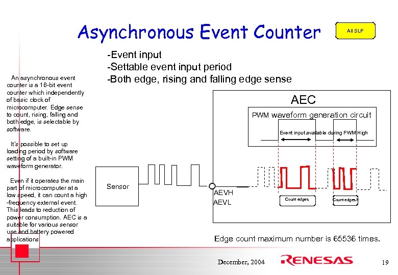 Asynchronous Event Counter An asynchronous event counter is a 16 -bit event counter which independently of basic clock of microcomputer. Edge sense to count, rising, falling and both edge, is selectable by software. All SLP -Event input -Settable event input period -Both edge, rising and falling edge sense AEC PWM waveform generation circuit Event input available during PWM High It’s possible to set up loading period by software setting of a built-in PWM waveform generator. Even if it operates the main part of microcomputer at a low speed, it can count a high -frequency external event. This leads to reduction of power consumption. AEC is a suitable for various sensor use and battery powered applications Sensor AEVH AEVL Count edgesト Edge count maximum number is 65536 times. December, 2004 19
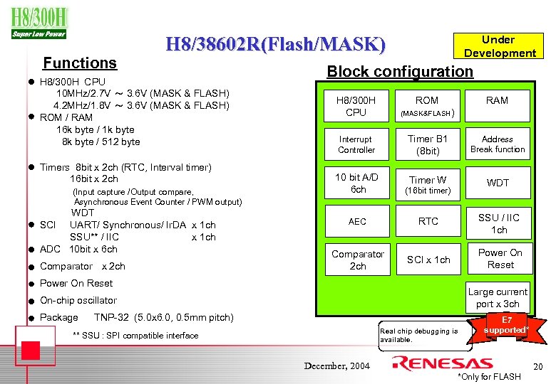 Functions H 8/38602 R(Flash/MASK) H 8/300 H CPU 10 MHz/2. 7 V ~ 3. 6 V (MASK & FLASH) 4. 2 MHz/1. 8 V ~ 3. 6 V (MASK & FLASH) ROM / RAM 16 k byte / 1 k byte 8 k byte / 512 byte Timers 8 bit x 2 ch (RTC, Interval timer) 16 bit x 2 ch (Input capture /Output compare, Under Development Block configuration H 8/300 H CPU ROM RAM (MASK&FLASH) Interrupt Controller Timer B 1 (8 bit) Address Break function 10 bit A/D 6 ch Timer W (16 bit timer) WDT AEC RTC SSU / IIC 1 ch Comparator 2 ch SCI x 1 ch Power On Reset Asynchronous Event Counter / PWM output) WDT SCI UART/ Synchronous/ Ir. DA x 1 ch SSU** / IIC x 1 ch ADC 10 bit x 6 ch Comparator x 2 ch Power On Reset Large current port x 3 ch On-chip oscillator Package TNP-32 (5. 0 x 6. 0, 0. 5 mm pitch) Real chip debugging is available. ** SSU : SPI compatible interface E 7 supported* December, 2004 20 *Only for FLASH


