

0eb5f351f3ed9b5807caef359e22c548.ppt
- Количество слайдов: 38
 Grid. Pix for Dual Phase LAr/LXe experiments
 Micro Patterned Gaseous Detectors GEM • High field created by Gas Gain Grids • Most popular: GEM & Micromegas Ideally: each grid hole red out by a pad Pad size ~ hole pitch ! VLSI pixel readout chip
 1. 2 mm Grid. Pix and Gas On Slimmed SIlicon Pixels Gossip: replacement of Si tracker Essential: thin gas layer (1. 2 mm)
 The Medi. Pix 2 pixel CMOS chip 256 x 256 pixels pixel: 55 x 55 μm 2 per pixel: - preamp - shaper - 2 discr. - Thresh. DAQ - 14 bit counter - enable counting - stop counting - readout image frame - reset We apply the ‘naked’ Medi. Pix 2 chip without X-ray convertor!
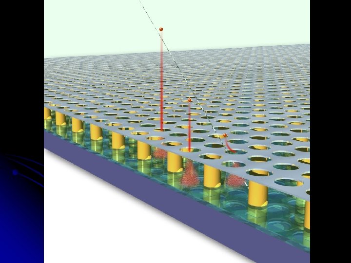
 Wafer post-processing: In. Grid Hex / Pillars Grids Silicon wafer HV biasing In. Grid: an Integrated Grid on Si (wafers or chips) l l perfect alignment of grid holes and pixel pads small pillars Ø, hidden pillars, full pixel area coverage Sub-micron precision: homogeneity Monolithic readout device: integrated electron amplifier
 Full post-processing of a Time. Pix • Timepix chip + Si. Prot + Ingrid: 14 mm MESA+ “Uniform” IMT Neuchatel Charge mode
 A “scratch” occurred during the construction of Ingrid; Loose parts removed. Ingrid working!
 90 Sr β events Gas: Ar/i-butane 80/20 B = 0. 2 T
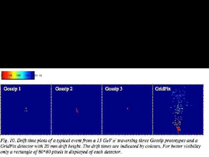
 Testbeam April 2008 PS/T 9: electrons and pions, 1 – 15 Ge. V/c L=30 mm V 0 V 1 f Transition Radiator 0. 05 mm
 and electrons (right) 6 Ge. V/c …broke Time. Pix") Particle Identification Samples pions (left) and electrons (right) 6 Ge. V/c …broke Time. Pix chip in Xe: 490 V on grid…
Particle Identification Samples pions (left) and electrons (right) 6 Ge. V/c …broke Time. Pix chip in Xe: 490 V on grid…
 Analysis of test beam data and cosmic muon data with Grid. Pix Colloquium Lucie de Nooij, Tuesday 13 January, 15 h, H 331
 First prototype of GOSSIP on a PSI 46") GOSSIP-Brico: PSI-46 (CMS Pixel FE chip) First prototype of GOSSIP on a PSI 46 is working: • 1. 2 mm drift gap • Grid signal used as trigger • 30 µm layer of Si. Prot
GOSSIP-Brico: PSI-46 (CMS Pixel FE chip) First prototype of GOSSIP on a PSI 46 is working: • 1. 2 mm drift gap • Grid signal used as trigger • 30 µm layer of Si. Prot
 7. 8 mm Animated") We can see tracks! (Frame # 17 is really great) 7. 8 mm Animated GIF of 100 hits on the PSI 46 brico, 30µm Si. Prot. (if this does not animate, drop the picture into a web browser)
We can see tracks! (Frame # 17 is really great) 7. 8 mm Animated GIF of 100 hits on the PSI 46 brico, 30µm Si. Prot. (if this does not animate, drop the picture into a web browser)
 Gas instead of Si Pro: - no radiation damage in sensor: gas is exchanged - modest pixel (analog) input circuitry: low power, little space - no bias current: simple input circuit - low detector material budget: 0. 06 % radiation length/layer typical: Si foil. New mechanical concepts - low power dissipation : little FE power (2 μW/pixel); no bias dissipation - operates at room temperature (but other temperatures are OK) - less sensitive for neutron and X-ray background - 3 D track info per layer if drift time is measured - gas is cheap (and very cheap wrt. Si sensors!), and light Con: - Gaseous chamber: discharges (sparks): destroy CMOS chip - gas-filled proportional chamber: ‘chamber ageing’ - limit in spatial resolution due to low primary gas-particle interaction statistics - Needs gas flow - Parallax error: 1 ns drift time measurement may be required - diffusion of (drifting) electrons in gas limit spatial resolution
 But, are these good enough? 2006 -2007 dead chips everywhere 2007 -2008 spark protection and Ingrid 2008 -2009 characterizing performance of Grid. Pix Cathode - Drift volume (~0. 1 -few k. V/cm) Grid - Gain region (~50 -150 k. V/cm) Pixel readout chip 17
, only 7") July 2008: protection layer made of Si 3 N 4 (Silicon Nitride), only 7 µm thick 3 Si. H 4 + 4 NH 3 Si 3 N 4 + 12 H 2 - Silicon Nitride is often applied as passivation layer: top finish of chips. - With overdose of Si. H 4: conductivity: high resistivity bulk material - Favored material for bearings in turbo chargers, jet engines 5 layers of Si 3 N 4 In. Grid + a-Si: H
July 2008: protection layer made of Si 3 N 4 (Silicon Nitride), only 7 µm thick 3 Si. H 4 + 4 NH 3 Si 3 N 4 + 12 H 2 - Silicon Nitride is often applied as passivation layer: top finish of chips. - With overdose of Si. H 4: conductivity: high resistivity bulk material - Favored material for bearings in turbo chargers, jet engines 5 layers of Si 3 N 4 In. Grid + a-Si: H
 studies: Martin Fransen") Discharge (protection) studies: Martin Fransen
Discharge (protection) studies: Martin Fransen
 Lorentz Force Skin Effect F=E. q I = ~ 3 A ! Improvement with Si Nitride
 discharges -discharges along non-protected") Chips still die after month of full-scale exposure (Thorium induced) discharges -discharges along non-protected paths (edges, peripherals) - Pinholes in Si 3 N 4 layer Highest priority to solve: !!!! In. Grid made of Si 3 N 4 !!!!
Chips still die after month of full-scale exposure (Thorium induced) discharges -discharges along non-protected paths (edges, peripherals) - Pinholes in Si 3 N 4 layer Highest priority to solve: !!!! In. Grid made of Si 3 N 4 !!!!
 Twin. Grid Gem. Grid Triple. Grid Gem. Grid with Si. O 2 insulator
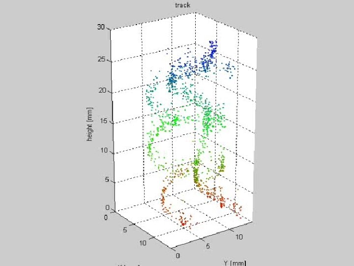
 Grid. Pix at Test Beam @ CERN Test of Gossip detector Low mass rad hard vertex detector. use ~1 mm gas instead of silicon Time. Pix chips 3 X Gossip and DICE in series DICE 19. 5 mm drift gap Gossips: 1 and 1. 5 mm drift 23
 gas mixture Not Gossip but Grid. Pix with 19.") l 1. Working point (cntd) gas mixture Not Gossip but Grid. Pix with 19. 3 mm drift gap Ar/i. C 4 H 10 80/20 (June 2009 testbeam) Our favourite is presently DME/CO 2 50/50 l Low diffusion (70 – 100 µm/√cm) l Low Lorentz angle (9º @ 2 T) l Good cluster density (45 cl/cm) l 125 electrons/cm CO 2/DME 50/50 09 20 ff. r be e- e m pte ingle Se s m %) a 8 tbe d (3 s Te ite Lim in agreement with simulations 80 pixels (4. 4 mm)
l 1. Working point (cntd) gas mixture Not Gossip but Grid. Pix with 19. 3 mm drift gap Ar/i. C 4 H 10 80/20 (June 2009 testbeam) Our favourite is presently DME/CO 2 50/50 l Low diffusion (70 – 100 µm/√cm) l Low Lorentz angle (9º @ 2 T) l Good cluster density (45 cl/cm) l 125 electrons/cm CO 2/DME 50/50 09 20 ff. r be e- e m pte ingle Se s m %) a 8 tbe d (3 s Te ite Lim in agreement with simulations 80 pixels (4. 4 mm)
 Electronics GOSSIPO-1: test of preamp-shaper-discriminator for GOSSIP ‘Multi. Project. Wafer’ in 0. 13 μm technology Cfb Input pad Cpar = 10 f. F… 50 f. F LM Iin(t) M 6 Ground plane Output M 2 M 1 Substrate Cpar A Output Open loop voltage gain of the OPAMP Ground M 3 Rfb Qin Cfb=1 f. F Very low (parasitic) capacitance at the input (Cpar → 10 f. F). Coaxial-like layout of the input Parasitic metal-to-metal interconnection. fringe capacitances.
 technology: isolation of digital and analog sections") Triple well layout in 130 nm (IBM) technology: isolation of digital and analog sections VDD_ana Guard rings Digital N-type FET area GND_ana GND Analog N-type FET area Analog P-type FET area P-well N-well substrate current P-type substrate
Triple well layout in 130 nm (IBM) technology: isolation of digital and analog sections VDD_ana Guard rings Digital N-type FET area GND_ana GND Analog N-type FET area Analog P-type FET area P-well N-well substrate current P-type substrate
 - match extreme small source capacity: 15 f. F - peaking time: 40 ns - noise (expected: 60 e- input eq. ) - power: 2 μW/pixel (!) GOSSIPO chip Submitted December 2005. - Input noise eq. reached - No effect of digital switching within pixel Multi. Project Wafer: Vladimir Gromov/NIKHEF CERN Micro-electronics group
 GOSSIPO-2 test of preamp-shaper-discriminator + 700 MHz TDC per pixel • 0. 13 μm technology • containing 16 x 16 pixels • Submission Nov 2006 • Can be used for GOSSIP demo!
 1 ns TDC per pixel Oscillator on pixel Time Over Threshold 40 MHz BX
 New CMOS pixel chip: Time. Pix-2 600 MHz osc in each pixel Low-noise, low power analog input Medipix-1 Medipix-2 Gossipo-2 MPW 250 nm technology Time. Pix Medipix-3 Time. Pix-2 130 nm technology Time. Pix-2: - TDC per pixel: σ = 1 ns - ‘ADC’ per pixel: Time. Over. Threshold - noise: 80 e- eq. - discharge protection circuit - fast (trigger enabled) readout Essentially ALL info on primary electrons in gas is extracted!
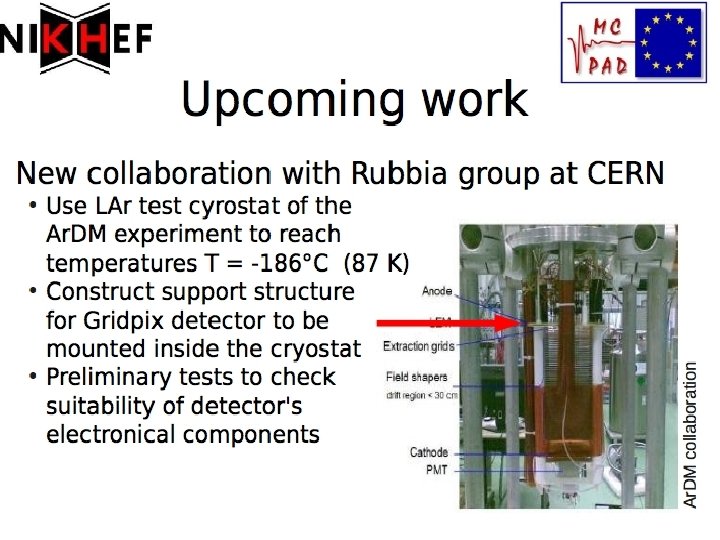
 WIMP search, bi-phase Xenon l Grid. Pix TPC as WIMP / DBD Source: Direct Searches for Dark Matter, Elena Aprile, EPS - HEP, July 21 2009, Krakow, Poland detector 4 th RD 51 Collaboration Meeting Maarten van Dijk
 Gridpix in Xenon: Test setup l Collaboration DARWIN/XENON Columbia Univ. , N. Y. 4 th RD 51 Collaboration Meeting Maarten van Dijk
 Now operational: UV photon Grid coated with 200 nm Cs. I mesh cathode with V = Vcat (gas ambient) primary e− SU‑ 8 pillar region with no or very low E field: transfer of primaries region with high E field: amplification region Joost Melay, Univ. Twente, MESA+ Jurriaan Schmitz’ STW project ‘There is plenty of room at the top’ With Amos Breskin, Weizmann Institute of Science in Rehovot, Israel ,
 Expanding Grid. Pix? l l Photoelectric effect Future possibility: Cs. I layer on grid 4 th RD 51 Collaboration Meeting Maarten van Dijk
 Photosensitive Grid. Pix Univ. Twente and Weizmann institute In. Grid with Cs. I on alu. anode Detect by means of gasgain Better anode readout Time. Pix UV light 200 -400 nm First test, In. Grid without Cs. I UV well absorbed by my fingerprint photon transfer of primary e− 38 mesh cathode In. Grid (Al) coated with 200 nm Cs. I