41bcd6c9eca34ad07e4954b0478082dc.ppt
- Количество слайдов: 40
General Semiconductor Packaging Process Flow Wafer Backgrinding, Die Preparation, Die Attach, Wire Bonding, Die Overcoat, Molding, Sealing, Marking, DTFS, Lead Finish, Electrical Testing, Tape & Reel, Dry Packing, Boxing and Labeling. DMT 243 – Chapter 3 M. Nuzaihan
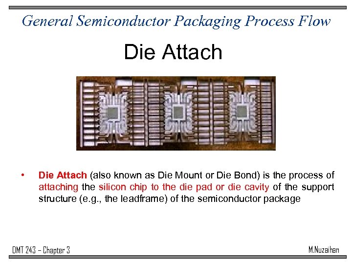
General Semiconductor Packaging Process Flow Die Attach • Die Attach (also known as Die Mount or Die Bond) is the process of attaching the silicon chip to the die pad or die cavity of the support structure (e. g. , the leadframe) of the semiconductor package DMT 243 – Chapter 3 M. Nuzaihan
General Semiconductor Packaging Process Flow Typical Die Attach Process Flow In high-volume production, die attach is performed on fully automated assembly equipment. The basic die attach steps, some of which are performed simultaneously, are: • A robotic loader picks up a lead frame from a stack and places it on the input area of the workholder. • The lead frame is moved from the input position to the dispense position. Depending on the required placement accuracy, mechanical or optical alignment points are used to define the dispense position. • Epoxy is dispensed in a pattern and volume appropriate for the chip size. • A sophisticated vision system inspects the lead frame, dispensing pattern and bond pads before the substrate is transported to the bonding position. DMT 243 – Chapter 3 M. Nuzaihan
General Semiconductor Packaging Process Flow Typical Die Attach Process Flow • In the meantime, a pattern recognition system locates a good die on the sawn wafer. • A vacuum pick-up tool mounted on a bond head grabs the aligned die from the wafer and places it on the programmed and pre-dispensed bond position on the substrate. • Appropriate bonding time and bonding force result in a strong bond, according to the specified process requirements. An additional optical inspection is performed to ensure that placement position and epoxy bleed-out requirements are met. • Each bond pad on the lead frame or substrate goes through this process before it is unloaded into an output magazine. DMT 243 – Chapter 3 M. Nuzaihan
General Semiconductor Packaging Process Flow Die Attach There are two common die attach processes, i. e. , adhesive die attach and eutectic die attach. Both of these processes use special die attach equipment and die attach tools to mount the die. For high-powered applications, the die is usually eutectic bonded onto the package (for good heat conduction). For low-cost, low-powered applications, the die is often glued directly onto a substrate using an epoxy adhesive. DMT 243 – Chapter 3 M. Nuzaihan
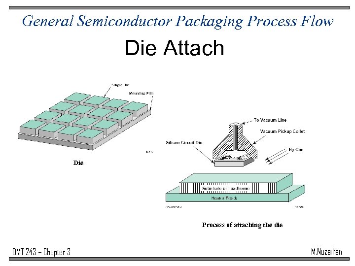
General Semiconductor Packaging Process Flow Die Attach Die Process of attaching the die DMT 243 – Chapter 3 M. Nuzaihan
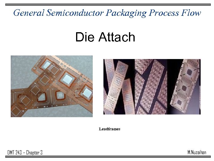
General Semiconductor Packaging Process Flow Die Attach Leadframes DMT 243 – Chapter 3 M. Nuzaihan
General Semiconductor Packaging Process Flow Adhesive Die Attach • Adhesive die attach uses adhesives such as polyimide, epoxy and silver-filled glass as die attach material to mount the die on the die pad or cavity. • The adhesive is first dispensed in controlled amounts on the die pad or cavity. • The die for mounting is then ejected from the wafer by one or more ejector needles. • While being ejected, a pick-and-place tool commonly known as a 'collet' then retrieves the die from the wafer tape and positions it on the adhesive. • All of the above steps are done by special die attach equipment or 'die bonders' DMT 243 – Chapter 3 M. Nuzaihan
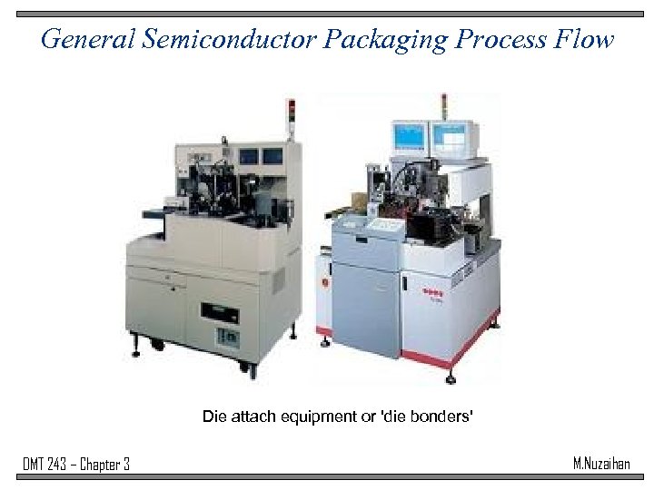
General Semiconductor Packaging Process Flow Die attach equipment or 'die bonders' DMT 243 – Chapter 3 M. Nuzaihan
General Semiconductor Packaging Process Flow Die Attach Tools Assignment 2 Group A 1 DMT 243 – Chapter 3 M. Nuzaihan
General Semiconductor Packaging Process Flow Adhesive Die Attach Advantages - Widely use as die attach materials in low-cost packaging application or plastic packaging. They are bonded at lower processing temperatures, reducing stress and providing a thermally and electrically conductive path from chip to the leadframe. Disadvantages of adhesive die attach material are that they are not thermally stable and absorb moisture, hence cannot be used in hermetically sealed package. DMT 243 – Chapter 3 M. Nuzaihan
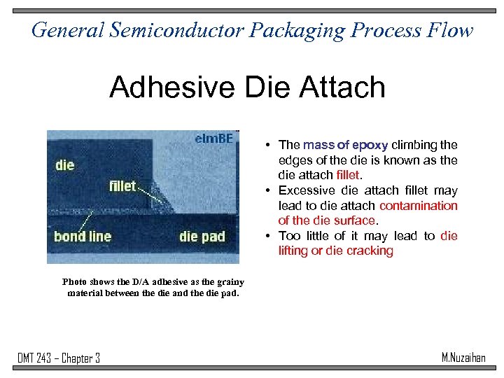
General Semiconductor Packaging Process Flow Adhesive Die Attach • The mass of epoxy climbing the edges of the die is known as the die attach fillet. • Excessive die attach fillet may lead to die attach contamination of the die surface. • Too little of it may lead to die lifting or die cracking Photo shows the D/A adhesive as the grainy material between the die and the die pad. DMT 243 – Chapter 3 M. Nuzaihan
General Semiconductor Packaging Process Flow Adhesive Die Attach Another critical aspect of adhesive die attach is the ejection of the die from the wafer tape during the pick-and-place system's retrieval operation. The use of inappropriate or worn-out ejector needle and improper ejection parameter settings can cause die backside tool marks or microcracks that can eventually lead to die cracking. DMT 243 – Chapter 3 M. Nuzaihan
General Semiconductor Packaging Process Flow Adhesive Die Attach Another critical aspect of adhesive die attach is the ejection of the die from the wafer tape during the pick-and-place system's retrieval operation. The use of inappropriate or worn-out ejector needle and improper ejection parameter settings can cause die backside tool marks or microcracks that can eventually lead to die cracking. DMT 243 – Chapter 3 M. Nuzaihan
General Semiconductor Packaging Process Flow Eutectic Die Attach Assignment 2 Group B 1 DMT 243 – Chapter 3 M. Nuzaihan
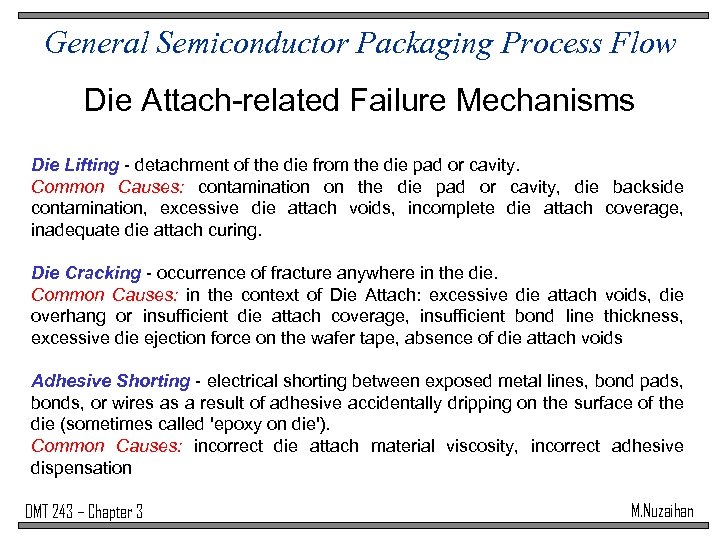
General Semiconductor Packaging Process Flow Die Attach-related Failure Mechanisms Die Lifting - detachment of the die from the die pad or cavity. Common Causes: contamination on the die pad or cavity, die backside contamination, excessive die attach voids, incomplete die attach coverage, inadequate die attach curing. Die Cracking - occurrence of fracture anywhere in the die. Common Causes: in the context of Die Attach: excessive die attach voids, die overhang or insufficient die attach coverage, insufficient bond line thickness, excessive die ejection force on the wafer tape, absence of die attach voids Adhesive Shorting - electrical shorting between exposed metal lines, bond pads, bonds, or wires as a result of adhesive accidentally dripping on the surface of the die (sometimes called 'epoxy on die'). Common Causes: incorrect die attach material viscosity, incorrect adhesive dispensation DMT 243 – Chapter 3 M. Nuzaihan
General Semiconductor Packaging Process Flow Die Attach-related Failure Mechanisms Bond Lifting - lifting of the first or second bond from the die or leadfinger, respectively. From the die attach process point of view, this is often due to resin bleeding of the die attach material into the bond pads or leadfingers, inhibiting good intermetallic formation. See also Wirebonding. Die Scratching - inducement of any mechanical damage on the die, as when an operator scratches a die with tweezers due to mishandling. Common Causes: insufficient operator training, worn-out or contaminated pick-andplace tool, disorderly workplace, use of improper tools Die Metallization Smearing - depression or deformation of any metal line on the die surface. Common Causes: dirty or worn-out die attach pick-and-place tool, wafer mishandling DMT 243 – Chapter 3 M. Nuzaihan
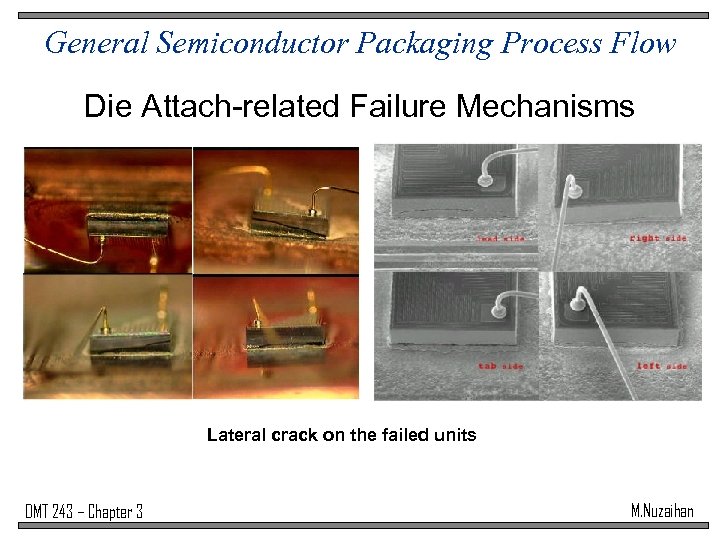
General Semiconductor Packaging Process Flow Die Attach-related Failure Mechanisms Lateral crack on the failed units DMT 243 – Chapter 3 M. Nuzaihan
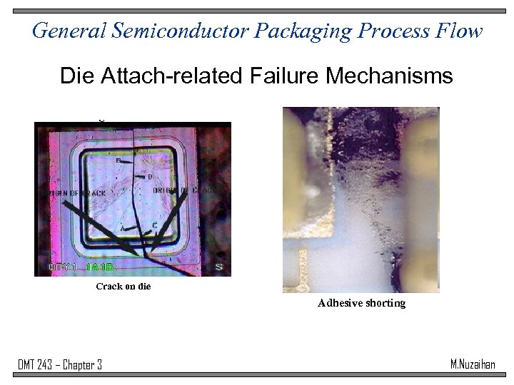
General Semiconductor Packaging Process Flow Die Attach-related Failure Mechanisms Crack on die Adhesive shorting DMT 243 – Chapter 3 M. Nuzaihan
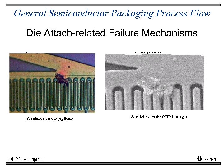
General Semiconductor Packaging Process Flow Die Attach-related Failure Mechanisms Scratches on die (optical) DMT 243 – Chapter 3 Scratches on die (SEM image) M. Nuzaihan
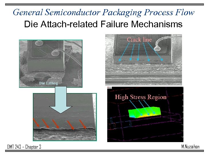
General Semiconductor Packaging Process Flow Die Attach-related Failure Mechanisms Die Lifting DMT 243 – Chapter 3 M. Nuzaihan
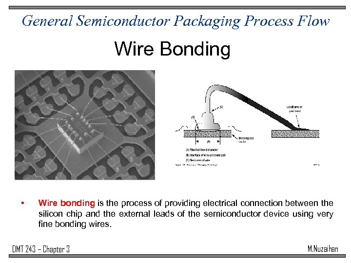
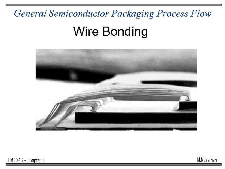
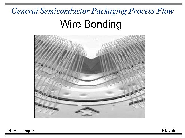
General Semiconductor Packaging Process Flow Wire Bonding • Wire bonding is the process of providing electrical connection between the silicon chip and the external leads of the semiconductor device using very fine bonding wires. DMT 243 – Chapter 3 M. Nuzaihan
General Semiconductor Packaging Process Flow Wire Bonding DMT 243 – Chapter 3 M. Nuzaihan
General Semiconductor Packaging Process Flow Wire Bonding DMT 243 – Chapter 3 M. Nuzaihan
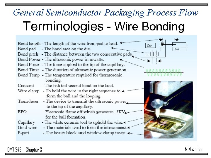
General Semiconductor Packaging Process Flow Terminologies - Wire Bonding DMT 243 – Chapter 3 M. Nuzaihan
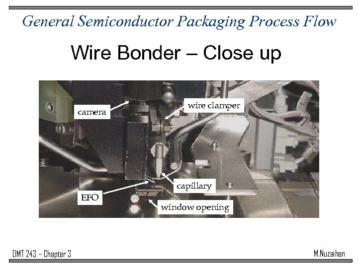
General Semiconductor Packaging Process Flow Wire Bonder – Close up camera wire clamper capillary EFO DMT 243 – Chapter 3 window opening M. Nuzaihan
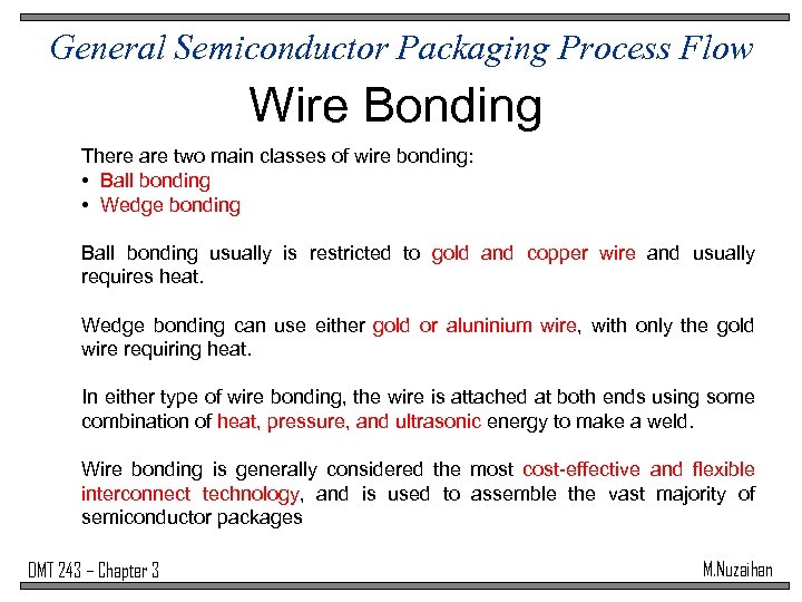
General Semiconductor Packaging Process Flow Wire Bonding There are two main classes of wire bonding: • Ball bonding • Wedge bonding Ball bonding usually is restricted to gold and copper wire and usually requires heat. Wedge bonding can use either gold or aluninium wire, with only the gold wire requiring heat. In either type of wire bonding, the wire is attached at both ends using some combination of heat, pressure, and ultrasonic energy to make a weld. Wire bonding is generally considered the most cost-effective and flexible interconnect technology, and is used to assemble the vast majority of semiconductor packages DMT 243 – Chapter 3 M. Nuzaihan
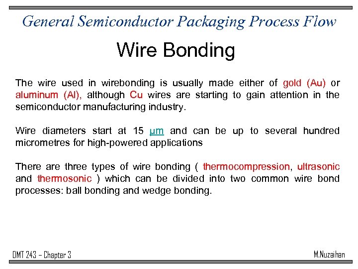
General Semiconductor Packaging Process Flow Wire Bonding The wire used in wirebonding is usually made either of gold (Au) or aluminum (Al), although Cu wires are starting to gain attention in the semiconductor manufacturing industry. Wire diameters start at 15 µm and can be up to several hundred micrometres for high-powered applications There are three types of wire bonding ( thermocompression, ultrasonic and thermosonic ) which can be divided into two common wire bond processes: ball bonding and wedge bonding. DMT 243 – Chapter 3 M. Nuzaihan
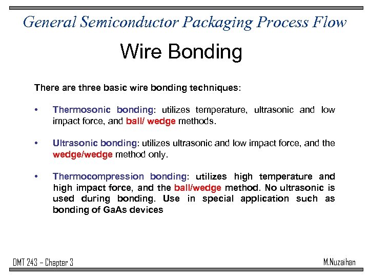
General Semiconductor Packaging Process Flow Wire Bonding There are three basic wire bonding techniques: • Thermosonic bonding: utilizes temperature, ultrasonic and low impact force, and ball/ wedge methods. • Ultrasonic bonding: utilizes ultrasonic and low impact force, and the wedge/wedge method only. • Thermocompression bonding: utilizes high temperature and high impact force, and the ball/wedge method. No ultrasonic is used during bonding. Use in special application such as bonding of Ga. As devices DMT 243 – Chapter 3 M. Nuzaihan
General Semiconductor Packaging Process Flow Thermosonic bonding Assignment 2 Group A 2 DMT 243 – Chapter 3 M. Nuzaihan
General Semiconductor Packaging Process Flow Ultrasonic bonding Assignment 2 Group B 2 DMT 243 – Chapter 3 M. Nuzaihan
General Semiconductor Packaging Process Flow Thermocompression bonding Assignment 2 Group A 3 DMT 243 – Chapter 3 M. Nuzaihan
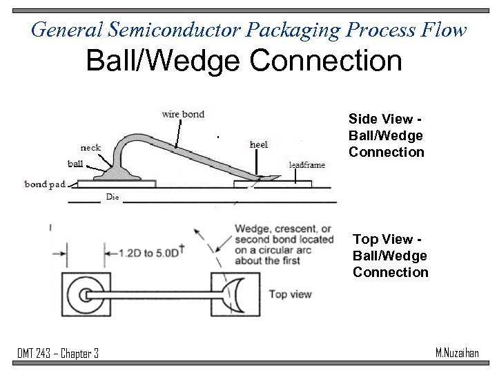
General Semiconductor Packaging Process Flow Ball/Wedge Connection Side View Ball/Wedge Connection Top View Ball/Wedge Connection DMT 243 – Chapter 3 M. Nuzaihan
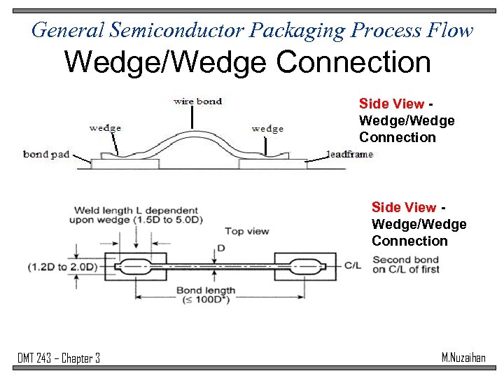
General Semiconductor Packaging Process Flow Wedge/Wedge Connection Side View Wedge/Wedge Connection DMT 243 – Chapter 3 M. Nuzaihan
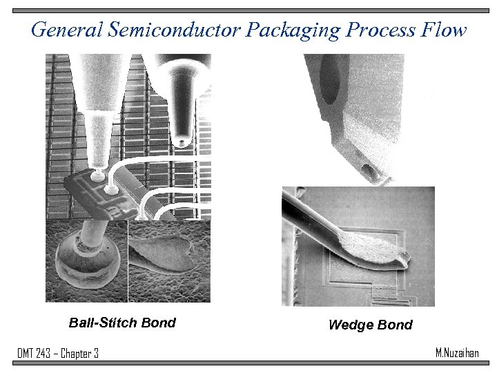
General Semiconductor Packaging Process Flow Ball-Stitch Bond DMT 243 – Chapter 3 Wedge Bond M. Nuzaihan
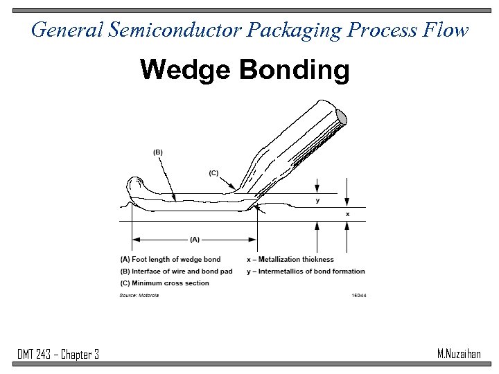
General Semiconductor Packaging Process Flow Wedge Bonding DMT 243 – Chapter 3 M. Nuzaihan
General Semiconductor Packaging Process Flow Wirebond - Important Parameters Assignment 2 Group A 1 DMT 243 – Chapter 3 M. Nuzaihan
General Semiconductor Packaging Process Flow Wirebond – Advanteges of Ball/Wedge and Wedge/wedge Assignment 2 Group B 1 DMT 243 – Chapter 3 M. Nuzaihan
General Semiconductor Packaging Process Flow Wirebond-related Failure Mechanisms Assignment 2 Group B 3 DMT 243 – Chapter 3 M. Nuzaihan
General Semiconductor Packaging Process Flow Next: Wafer Backgrinding, Die Preparation, Die Attach, Wire Bonding, Die Overcoat, Molding, Sealing, Marking, DTFS, Lead Finish, Electrical Testing, Tape & Reel, Dry Packing, Boxing and Labeling. DMT 243 – Chapter 3 M. Nuzaihan
41bcd6c9eca34ad07e4954b0478082dc.ppt