c9f54489d82d06a4e6dacb9c773359ec.ppt
- Количество слайдов: 30
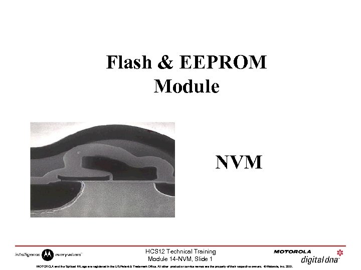 Flash & EEPROM Module NVM HCS 12 Technical Training Module 14 -NVM, Slide 1 MOTOROLA and the Stylized M Logo are registered in the US Patent & Trademark Office. All other product or service names are the property of their respective owners. © Motorola, Inc. 2001.
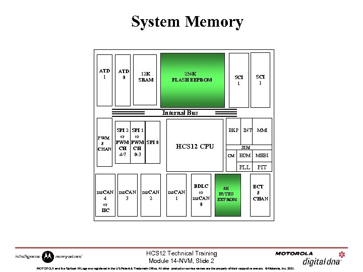 System Memory ATD 1 ATD 0 12 K SRAM 256 K FLASH EEPROM SCI 1 Internal Bus SPI 2 SPI 1 or or PWM PWM SPI 0 8 CH CH CHAN 4 -7 0 -3 BKP HCS 12 CPU INT MMI SIM ms. CAN 4 or IIC ms. CAN 3 ms. CAN 2 ms. CAN 1 BDLC or ms. CAN 0 4 K BYTES EEPROM BDM MEBI PLL CM PIT ECT 8 CHAN HCS 12 Technical Training Module 14 -NVM, Slide 2 MOTOROLA and the Stylized M Logo are registered in the US Patent & Trademark Office. All other product or service names are the property of their respective owners. © Motorola, Inc. 2001.
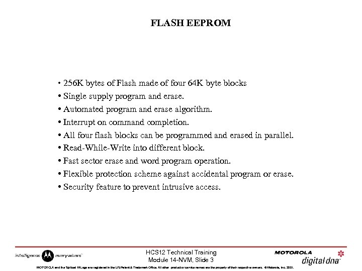 FLASH EEPROM • 256 K bytes of Flash made of four 64 K byte blocks • Single supply program and erase. • Automated program and erase algorithm. • Interrupt on command completion. • All four flash blocks can be programmed and erased in parallel. • Read-While-Write into different block. • Fast sector erase and word program operation. • Flexible protection scheme against accidental program or erase. • Security feature to prevent intrusive access. HCS 12 Technical Training Module 14 -NVM, Slide 3 MOTOROLA and the Stylized M Logo are registered in the US Patent & Trademark Office. All other product or service names are the property of their respective owners. © Motorola, Inc. 2001.
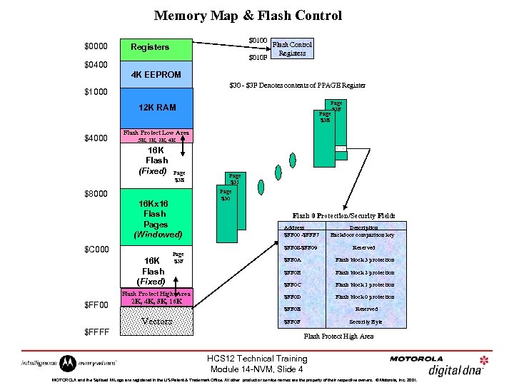 Memory Map & Flash Control $0000 $0100 Registers $010 F $0400 Flash Control Registers 4 K EEPROM $30 - $3 F Denotes contents of PPAGE Register $1000 Page $3 F Page $3 E 12 K RAM $4000 Flash Protect Low Area. 5 K, 1 K, 2 K, 4 K 16 K Flash (Fixed) Page $3 E $8000 16 Kx 16 Flash Pages (Windowed) 16 K Flash (Fixed) Page $3 F Flash Protect High Area 2 K, 4 K, 8 K, 16 K Flash 0 Protection/Security Fields Address $FF 00 -$FFF 7 Description Backdoor comparison key Reserved $FF 0 A Flash block 3 protection $FF 0 B Flash block 2 protection $FF 0 C Flash block 1 protection $FF 0 D Flash block 0 protection $FF 0 E Vectors $FFFF Page $30 $FF 08 -$FF 09 $C 000 $FF 00 Page $31 Reserved $FF 0 F Security Byte Flash Protect High Area HCS 12 Technical Training Module 14 -NVM, Slide 4 MOTOROLA and the Stylized M Logo are registered in the US Patent & Trademark Office. All other product or service names are the property of their respective owners. © Motorola, Inc. 2001.
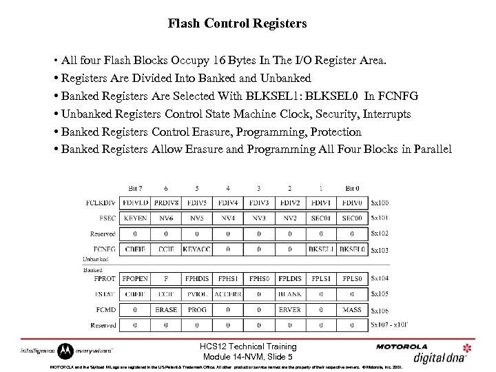 Flash Control Registers • All four Flash Blocks Occupy 16 Bytes In The I/O Register Area. • Registers Are Divided Into Banked and Unbanked • Banked Registers Are Selected With BLKSEL 1: BLKSEL 0 In FCNFG • Unbanked Registers Control State Machine Clock, Security, Interrupts • Banked Registers Control Erasure, Programming, Protection • Banked Registers Allow Erasure and Programming All Four Blocks in Parallel HCS 12 Technical Training Module 14 -NVM, Slide 5 MOTOROLA and the Stylized M Logo are registered in the US Patent & Trademark Office. All other product or service names are the property of their respective owners. © Motorola, Inc. 2001.
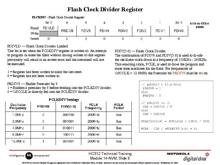 Flash Clock Divider Register FLCKDIV - Flash Clock Divider Register Address Offset $0000 FDIVLD — Flash Clock Divider Loaded This bit is set when the FCLKDIV register is written to. An attempt to program or erase the flash without having written to this register previously will result in an access error and the command will not be executed. 1 = Register has been written to since the last reset. 0 = Register has not been written to. FDIV[5: 0] — Flash Clock Divider The combination of FDIV 8 and FDIV[5: 0] is used to divide the oscillator clock down to a frequency of 150 KHz - 200 KHz. This resulting clock, FCLK, is used to drive the program and erase state machines for the flash. For frequencies of OSCCLK > 12. 8 MHz the Prescaler bit PRDIV 8 must be set on. PRDIV 8 — Enable Prescaler by 8 1 = Enables a prescaler by 8 before feeding into the FCLKDIV divider. 0 = OSCCLK is directly fed into the FCLKDIV divider FCLKDIV Settings HCS 12 Technical Training Module 14 -NVM, Slide 6 MOTOROLA and the Stylized M Logo are registered in the US Patent & Trademark Office. All other product or service names are the property of their respective owners. © Motorola, Inc. 2001.
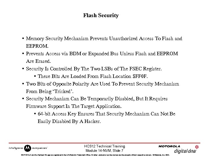 Flash Security • Memory Security Mechanism Prevents Unauthorized Access To Flash and EEPROM. • Prevents Access via BDM or Expanded Bus Unless Flash and EEPROM Are Erased. • Security Is Controlled By The Two LSBs of The FSEC Register. • These Bits Are Loaded From Flash Location $FF 0 F. • Two Bits of Opposite Polarity Are Used To Prevent Security Mechanism From Being ‘Tricked’. • Security Mechanism Can Be Temporarily Disabled, But It Requires Firmware Support In The Target Application. • 64 -bit Access Key Ensures That Security Mechanism Can Not Be Easily Disabled By A Hacker. HCS 12 Technical Training Module 14 -NVM, Slide 7 MOTOROLA and the Stylized M Logo are registered in the US Patent & Trademark Office. All other product or service names are the property of their respective owners. © Motorola, Inc. 2001.
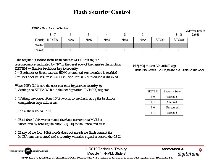 Flash Security Control FSEC - Flash Security Register Address Offset $x 001 This register is loaded from flash address $FF 0 F during the reset sequence, indicated by “F” in the reset row of the register description. KEYEN — Enable backdoor key to security 1 = Backdoor to flash read via BDM or external bus interface is enabled 0 = Backdoor to flash read via BDM or external bus interface is disabled. NV[6: 2] = Non-Volatile Flags These Non-Volatile Flags are available to the user When KEYEN is set, the user can then bypass the security by: 1. Setting the KEYACC bit in the configuration (FCNFG) register. 2. Writing the correct four 16 bit words to the flash using the backdoor comparison keys addresses. 3. Clear the KEYACC bit. 4. If all four 16 bit words match the flash content, the MCU is unsecured by forcing the bits SEC[1: 0] to the unsecured state. 5. If any of the four 16 bit words does not match the flash content the MCU remains secured and a security violation signal is sent to the CPU. HCS 12 Technical Training Module 14 -NVM, Slide 8 MOTOROLA and the Stylized M Logo are registered in the US Patent & Trademark Office. All other product or service names are the property of their respective owners. © Motorola, Inc. 2001.
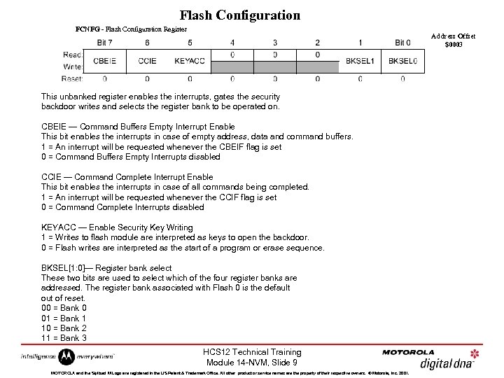 Flash Configuration FCNFG - Flash Configuration Register Address Offset $0003 This unbanked register enables the interrupts, gates the security backdoor writes and selects the register bank to be operated on. CBEIE — Command Buffers Empty Interrupt Enable This bit enables the interrupts in case of empty address, data and command buffers. 1 = An interrupt will be requested whenever the CBEIF flag is set 0 = Command Buffers Empty Interrupts disabled CCIE — Command Complete Interrupt Enable This bit enables the interrupts in case of all commands being completed. 1 = An interrupt will be requested whenever the CCIF flag is set 0 = Command Complete Interrupts disabled KEYACC — Enable Security Key Writing 1 = Writes to flash module are interpreted as keys to open the backdoor. 0 = Flash writes are interpreted as the start of a program or erase sequence. BKSEL[1: 0]— Register bank select These two bits are used to select which of the four register banks are addressed. The register bank associated with Flash 0 is the default out of reset. 00 = Bank 0 01 = Bank 1 10 = Bank 2 11 = Bank 3 HCS 12 Technical Training Module 14 -NVM, Slide 9 MOTOROLA and the Stylized M Logo are registered in the US Patent & Trademark Office. All other product or service names are the property of their respective owners. © Motorola, Inc. 2001.
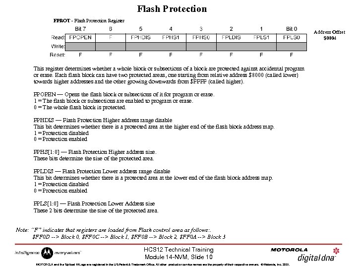 Flash Protection FPROT - Flash Protection Register Address Offset $0004 This register determines whether a whole block or subsections of a block are protected against accidental program or erase. Each flash block can have two protected areas, one starting from relative address $8000 (called lower) towards higher addresses and the other growing downwards from $FFFF (called higher). FPOPEN — Opens the flash block or subsections of it for program or erase. 1 = The flash block or subsections are enabled to program or erase. 0 = The whole flash block is protected. FPHDIS — Flash Protection Higher address range disable This bit determines whethere is a protected area at the higher end of the flash block address map. 1 = Protection disabled 0 = Protection enabled FPHS[1: 0] — Flash Protection Higher address size. These bits determine the size of the protected area. FPLDIS — Flash Protection Lower address range disable This bit determines whethere is a protected area at the lower end of the flash block address map. 1 = Protection disabled 0 = Protection enabled FPLS[1: 0] — Flash Protection Lower Address size These 2 bits determine the size of the protected area. Note: “F” indicates that registers are loaded from Flash control area as follows: . $FF 0 D --> Block 0, $FF 0 C --> Block 1, $FF 0 B --> Block 2, $FF 0 A --> Block 3 HCS 12 Technical Training Module 14 -NVM, Slide 10 MOTOROLA and the Stylized M Logo are registered in the US Patent & Trademark Office. All other product or service names are the property of their respective owners. © Motorola, Inc. 2001.
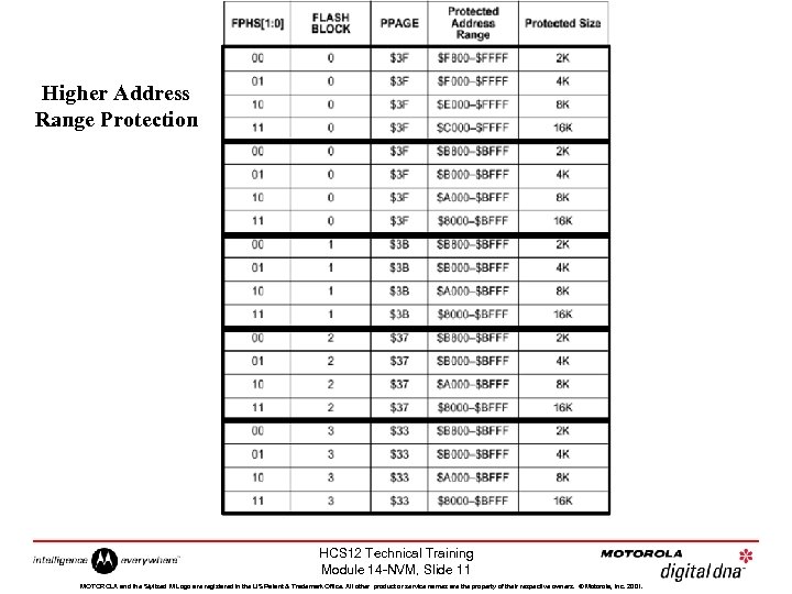 Higher Address Range Protection HCS 12 Technical Training Module 14 -NVM, Slide 11 MOTOROLA and the Stylized M Logo are registered in the US Patent & Trademark Office. All other product or service names are the property of their respective owners. © Motorola, Inc. 2001.
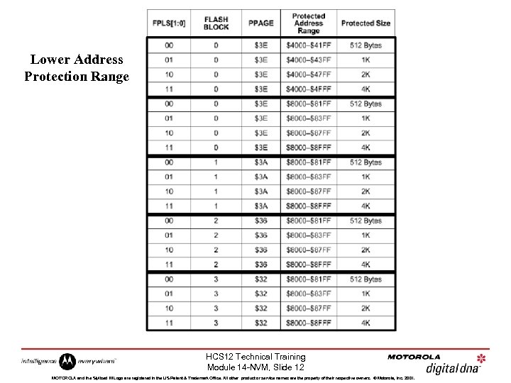 Lower Address Protection Range HCS 12 Technical Training Module 14 -NVM, Slide 12 MOTOROLA and the Stylized M Logo are registered in the US Patent & Trademark Office. All other product or service names are the property of their respective owners. © Motorola, Inc. 2001.
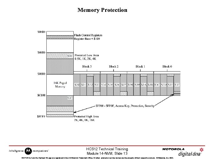 Memory Protection HCS 12 Technical Training Module 14 -NVM, Slide 13 MOTOROLA and the Stylized M Logo are registered in the US Patent & Trademark Office. All other product or service names are the property of their respective owners. © Motorola, Inc. 2001.
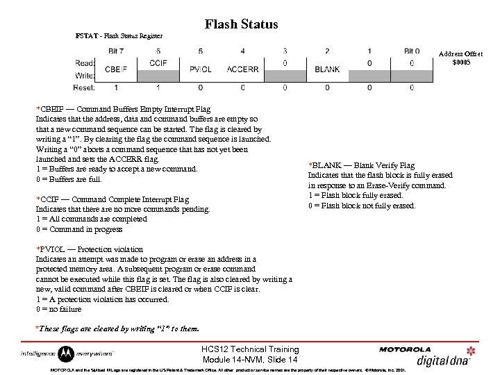 Flash Status FSTAT - Flash Status Register Address Offset $0005 *CBEIF — Command Buffers Empty Interrupt Flag Indicates that the address, data and command buffers are empty so that a new command sequence can be started. The flag is cleared by writing a “ 1”. By clearing the flag the command sequence is launched. Writing a “ 0” aborts a command sequence that has not yet been launched and sets the ACCERR flag. 1 = Buffers are ready to accept a new command. 0 = Buffers are full. *CCIF — Command Complete Interrupt Flag Indicates that there are no more commands pending. 1 = All commands are completed 0 = Command in progress *BLANK — Blank Verify Flag Indicates that the flash block is fully erased in response to an Erase-Verify command. 1 = Flash block fully erased. 0 = Flash block not fully erased. *PVIOL — Protection violation Indicates an attempt was made to program or erase an address in a protected memory area. A subsequent program or erase command cannot be executed while this flag is set. The flag is also cleared by writing a new, valid command after CBEIF is cleared or when CCIF is clear. 1 = A protection violation has occurred. 0 = no failure *These flags are cleared by writing “ 1” to them. HCS 12 Technical Training Module 14 -NVM, Slide 14 MOTOROLA and the Stylized M Logo are registered in the US Patent & Trademark Office. All other product or service names are the property of their respective owners. © Motorola, Inc. 2001.
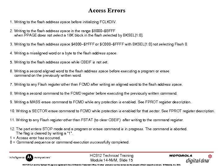 Access Errors 1. Writing to the flash address space before initializing FCLKDIV. 2. Writing to the flash address space in the range $8000–$BFFF when PPAGE does not select a 16 K block in the flash selected by BKSEL[1: 0]. 3. Writing to the flash address space $4000–$7 FFF or $C 000–$FFFF with BKSEL[1: 0] not selecting Flash 0. 4. Writing a misaligned word or a byte to the flash address space. 5. Writing to the flash address space while CBEIF is not set. 6. Writing a second aligned word to the flash address space before executing a program or erase command on the previously written word. 7. Writing to any Flash register other than FCMD after writing an aligned word to the flash address space. 8. Writing a second command to the FCMD register before executing the previously written command. 9. Writing a MASS erase command to FCMD while any protection is enabled. See FPROT register description. 10. Writing a SECTOR erase command to FCMD while protection is enabled for that sector. See FPROT register description. 11. Writing to any Flash register other than FSTAT (to clear CBEIF) after writing to the command register. 12. The part enters STOP mode and a program or erase command is in progress. The command is aborted. The flag is cleared by writing a “ 1”. 1 = Access error has occurred. 0 = Command sequence or command execution successfully completed. HCS 12 Technical Training Module 14 -NVM, Slide 15 MOTOROLA and the Stylized M Logo are registered in the US Patent & Trademark Office. All other product or service names are the property of their respective owners. © Motorola, Inc. 2001.
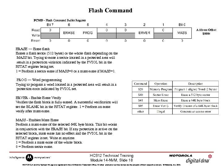 Flash Command FCMD - Flash Command Buffer Register Address Offset $0006 ERASE — Erase flash Erases a flash sector (512 bytes) or the whole flash depending on the MASS bit. Trying to erase a sector located in a protected area will result in a protection violation indicated by the PVIOL bit in the FSTAT register being set. 1 = Perform a sector erase if MASS=0 or a mass erase if MASS=1. PROG — Word programming Trying to program a word located in a protected area will result in a protection error indicated by PVIOL set. ERVER - Enable Erase Verify Verifies the flash block is fully erased. A successful verification will set the BLANK bit in the FSTAT register. 1 = Perform an erase verify after mass erase. MASS - Enables Mass Erase Perform a mass erase of the selected 64 K byte block. This bit works in conjunction with the ERASE bit. If any protection is active on the selected block, mass erase has no effect and the PVIOL bit in the FSTAT register is set. Write at anytime. 1 = Perform a mass erase of the whole block. 0 = Perform sector erase. HCS 12 Technical Training Module 14 -NVM, Slide 16 MOTOROLA and the Stylized M Logo are registered in the US Patent & Trademark Office. All other product or service names are the property of their respective owners. © Motorola, Inc. 2001.
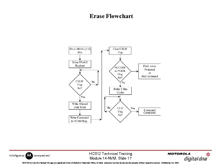 Erase Flowchart HCS 12 Technical Training Module 14 -NVM, Slide 17 MOTOROLA and the Stylized M Logo are registered in the US Patent & Trademark Office. All other product or service names are the property of their respective owners. © Motorola, Inc. 2001.
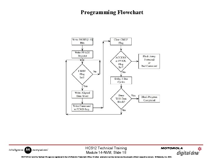 Programming Flowchart HCS 12 Technical Training Module 14 -NVM, Slide 18 MOTOROLA and the Stylized M Logo are registered in the US Patent & Trademark Office. All other product or service names are the property of their respective owners. © Motorola, Inc. 2001.
 EEPROM 4 K BYTE HCS 12 Technical Training Module 14 -NVM, Slide 19 MOTOROLA and the Stylized M Logo are registered in the US Patent & Trademark Office. All other product or service names are the property of their respective owners. © Motorola, Inc. 2001.
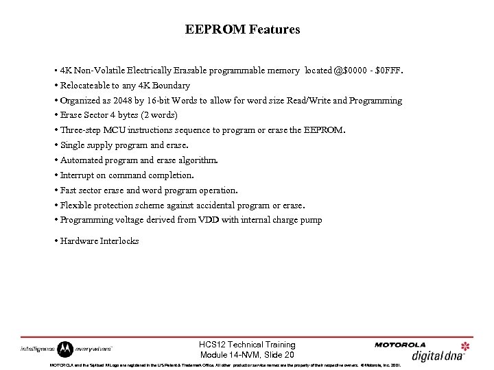 EEPROM Features • 4 K Non-Volatile Electrically Erasable programmable memory located @$0000 - $0 FFF. • Relocateable to any 4 K Boundary • Organized as 2048 by 16 -bit Words to allow for word size Read/Write and Programming • Erase Sector 4 bytes (2 words) • Three-step MCU instructions sequence to program or erase the EEPROM. • Single supply program and erase. • Automated program and erase algorithm. • Interrupt on command completion. • Fast sector erase and word program operation. • Flexible protection scheme against accidental program or erase. • Programming voltage derived from VDD with internal charge pump • Hardware Interlocks HCS 12 Technical Training Module 14 -NVM, Slide 20 MOTOROLA and the Stylized M Logo are registered in the US Patent & Trademark Office. All other product or service names are the property of their respective owners. © Motorola, Inc. 2001.
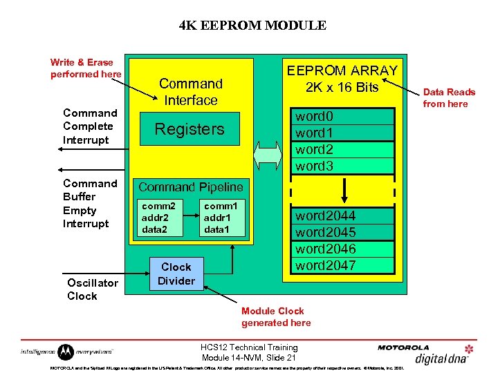 4 K EEPROM MODULE Write & Erase performed here Command Complete Interrupt Command Buffer Empty Interrupt Oscillator Clock EEPROM ARRAY 2 K x 16 Bits Command Interface word 0 word 1 word 2 word 3 Registers Command Pipeline comm 2 addr 2 data 2 Clock Divider comm 1 addr 1 data 1 word 2044 word 2045 word 2046 word 2047 Module Clock generated here HCS 12 Technical Training Module 14 -NVM, Slide 21 MOTOROLA and the Stylized M Logo are registered in the US Patent & Trademark Office. All other product or service names are the property of their respective owners. © Motorola, Inc. 2001. Data Reads from here
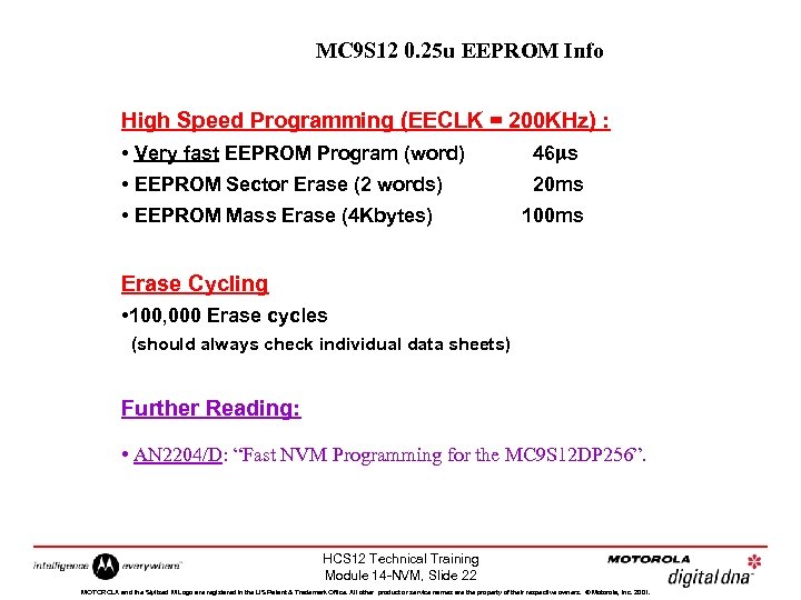 MC 9 S 12 0. 25 u EEPROM Info High Speed Programming (EECLK = 200 KHz) : • Very fast EEPROM Program (word) 46 ms • EEPROM Sector Erase (2 words) 20 ms • EEPROM Mass Erase (4 Kbytes) 100 ms Erase Cycling • 100, 000 Erase cycles (should always check individual data sheets) Further Reading: • AN 2204/D: “Fast NVM Programming for the MC 9 S 12 DP 256”. HCS 12 Technical Training Module 14 -NVM, Slide 22 MOTOROLA and the Stylized M Logo are registered in the US Patent & Trademark Office. All other product or service names are the property of their respective owners. © Motorola, Inc. 2001.
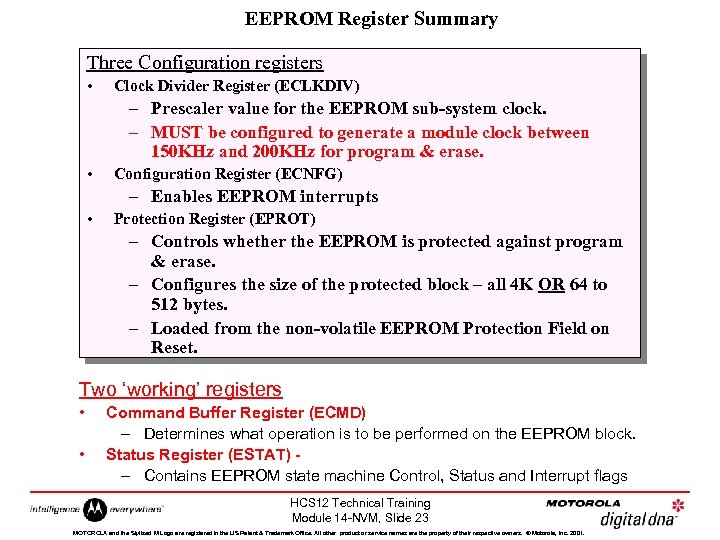 EEPROM Register Summary Three Configuration registers • Clock Divider Register (ECLKDIV) – Prescaler value for the EEPROM sub-system clock. – MUST be configured to generate a module clock between 150 KHz and 200 KHz for program & erase. • Configuration Register (ECNFG) – Enables EEPROM interrupts • Protection Register (EPROT) – Controls whether the EEPROM is protected against program & erase. – Configures the size of the protected block – all 4 K OR 64 to 512 bytes. – Loaded from the non-volatile EEPROM Protection Field on Reset. Two ‘working’ registers • • Command Buffer Register (ECMD) – Determines what operation is to be performed on the EEPROM block. Status Register (ESTAT) – Contains EEPROM state machine Control, Status and Interrupt flags HCS 12 Technical Training Module 14 -NVM, Slide 23 MOTOROLA and the Stylized M Logo are registered in the US Patent & Trademark Office. All other product or service names are the property of their respective owners. © Motorola, Inc. 2001.
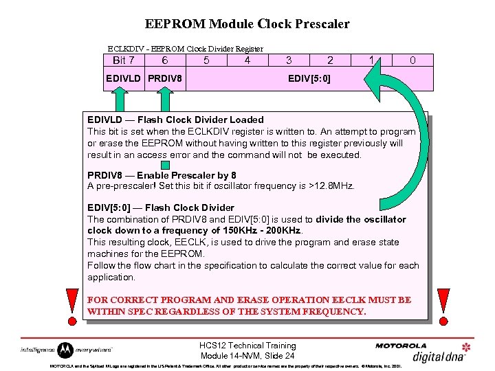 EEPROM Module Clock Prescaler ECLKDIV - EEPROM Clock Divider Register Bit 7 6 EDIVLD PRDIV 8 5 4 3 2 1 0 EDIV[5: 0] EDIVLD — Flash Clock Divider Loaded This bit is set when the ECLKDIV register is written to. An attempt to program or erase the EEPROM without having written to this register previously will result in an access error and the command will not be executed. PRDIV 8 — Enable Prescaler by 8 A pre-prescaler! Set this bit if oscillator frequency is >12. 8 MHz. EDIV[5: 0] — Flash Clock Divider The combination of PRDIV 8 and EDIV[5: 0] is used to divide the oscillator clock down to a frequency of 150 KHz - 200 KHz. This resulting clock, EECLK, is used to drive the program and erase state machines for the EEPROM. Follow the flow chart in the specification to calculate the correct value for each application. FOR CORRECT PROGRAM AND ERASE OPERATION EECLK MUST BE WITHIN SPEC REGARDLESS OF THE SYSTEM FREQUENCY. HCS 12 Technical Training Module 14 -NVM, Slide 24 MOTOROLA and the Stylized M Logo are registered in the US Patent & Trademark Office. All other product or service names are the property of their respective owners. © Motorola, Inc. 2001.
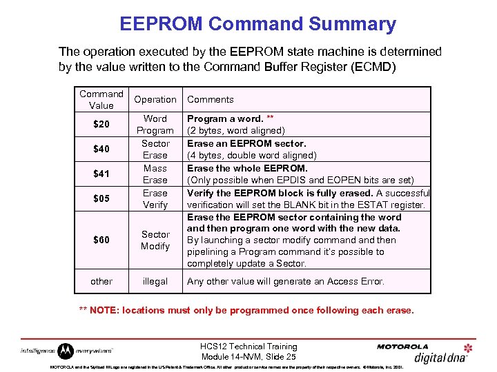 EEPROM Command Summary The operation executed by the EEPROM state machine is determined by the value written to the Command Buffer Register (ECMD) Command Value $20 $41 $05 Operation Comments Word Program Sector Erase Mass Erase Verify Program a word. ** (2 bytes, word aligned) Erase an EEPROM sector. (4 bytes, double word aligned) Erase the whole EEPROM. (Only possible when EPDIS and EOPEN bits are set) Verify the EEPROM block is fully erased. A successful verification will set the BLANK bit in the ESTAT register. Erase the EEPROM sector containing the word and then program one word with the new data. By launching a sector modify command then pipelining a Program command it’s possible to completely update a Sector. $60 Sector Modify other illegal Any other value will generate an Access Error. ** NOTE: locations must only be programmed once following each erase. HCS 12 Technical Training Module 14 -NVM, Slide 25 MOTOROLA and the Stylized M Logo are registered in the US Patent & Trademark Office. All other product or service names are the property of their respective owners. © Motorola, Inc. 2001.
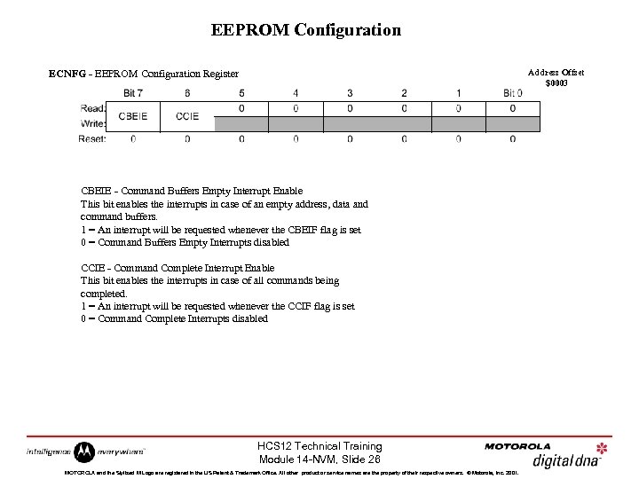 EEPROM Configuration Address Offset $0003 ECNFG - EEPROM Configuration Register CBEIE - Command Buffers Empty Interrupt Enable This bit enables the interrupts in case of an empty address, data and command buffers. 1 = An interrupt will be requested whenever the CBEIF flag is set 0 = Command Buffers Empty Interrupts disabled CCIE - Command Complete Interrupt Enable This bit enables the interrupts in case of all commands being completed. 1 = An interrupt will be requested whenever the CCIF flag is set 0 = Command Complete Interrupts disabled HCS 12 Technical Training Module 14 -NVM, Slide 26 MOTOROLA and the Stylized M Logo are registered in the US Patent & Trademark Office. All other product or service names are the property of their respective owners. © Motorola, Inc. 2001.
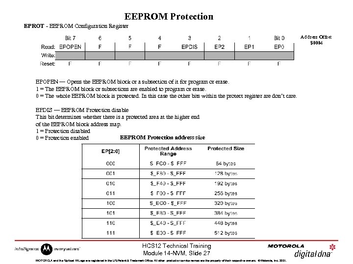 EEPROM Protection EPROT - EEPROM Configuration Register Address Offset $0004 EPOPEN — Opens the EEPROM block or a subsection of it for program or erase. 1 = The EEPROM block or subsections are enabled to program or erase. 0 = The whole EEPROM block is protected. In this case the other bits within the protect register are don’t care. EPDIS — EEPROM Protection disable This bit determines whethere is a protected area at the higher end of the EEPROM block address map. 1 = Protection disabled EEPROM Protection address size 0 = Protection enabled HCS 12 Technical Training Module 14 -NVM, Slide 27 MOTOROLA and the Stylized M Logo are registered in the US Patent & Trademark Office. All other product or service names are the property of their respective owners. © Motorola, Inc. 2001.
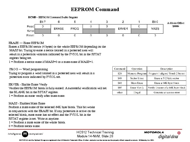 EEPROM Command ECMD - EEPROM Command Buffer Register Address Offset $0006 ERASE — Erase EEPROM Erases a EEPROM sector (4 bytes) or the whole EEPROM depending on the MASS bit. Trying to erase a sector located in a protected area will result in a protection violation indicated by the PVIOL bit in the FSTAT register being set. 1 = Perform a sector erase if MASS=0 or a mass erase if MASS=1. PROG — Word programming Trying to program a word located in a protected area will result in a protection error indicated by PVIOL set. ERVER - Enable Erase Verify Verifies the EEPROM block is fully erased. A successful verification will set the BLANK bit in the FSTAT register. 1 = Perform an erase verify after mass erase. MASS - Enables Mass Erase Perform a mass erase of the selected 64 K byte block. This bit works in conjunction with the ERASE bit. If any protection is active on the selected block, mass erase has no effect and the PVIOL bit in the FSTAT register is set. Write at anytime. 1 = Perform a mass erase of the whole block. 0 = Perform sector erase. HCS 12 Technical Training Module 14 -NVM, Slide 28 MOTOROLA and the Stylized M Logo are registered in the US Patent & Trademark Office. All other product or service names are the property of their respective owners. © Motorola, Inc. 2001.
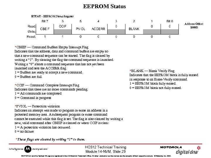 EEPROM Status ESTAT - EEPROM Status Register Address Offset $0005 *CBEIF — Command Buffers Empty Interrupt Flag Indicates that the address, data and command buffers are empty so that a new command sequence can be started. The flag is cleared by writing a “ 1”. By clearing the flag the command sequence is launched. Writing a “ 0” aborts a command sequence that has not yet been launched and sets the ACCERR flag. 1 = Buffers are ready to accept a new command. 0 = Buffers are full. *CCIF — Command Complete Interrupt Flag Indicates that there are no more commands pending. 1 = All commands are completed 0 = Command in progress *BLANK — Blank Verify Flag Indicates that the EEPROM block is fully erased in response to an Erase-Verify command. 1 = EEPROM block fully erased. 0 = EEPROM block not fully erased. *PVIOL — Protection violation Indicates an attempt was made to program or erase an address in a protected memory area. A subsequent program or erase command cannot be executed while this flag is set. The flag is also cleared by writing a new, valid command after CBEIF is cleared or when CCIF is clear. 1 = A protection violation has occurred. 0 = no failure *These flags are cleared by writing “ 1” to them. HCS 12 Technical Training Module 14 -NVM, Slide 29 MOTOROLA and the Stylized M Logo are registered in the US Patent & Trademark Office. All other product or service names are the property of their respective owners. © Motorola, Inc. 2001.
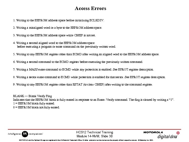 Access Errors 1. Writing to the EEPROM address space before initializing ECLKDIV. 2. Writing a misaligned word or a byte to the EEPROM address space. 3. Writing to the EEPROM address space while CBEIF is not set. 4. Writing a second aligned word to the EEPROM address space before executing a program or erase command on the previously written word. 5. Writing to any EEPROM register other than ECMD after writing an aligned word to the EEPROM address space. 6. Writing a second command to the ECMD register before executing the previously written command. 7. Writing a MASS erase command to ECMD while any protection is enabled. See EPROT register description. 8. Writing a sector erase command to ECMD while protection is enabled for that sector. See EPROT register description. 9. Writing to any EEPROM register other than ESTAT (to clear CBEIF) after writing to the command register. BLANK — Blank Verify Flag Indicates that the EEPROM block is fully erased in response to an Erase- Verify command. The flag is cleared by writing a “ 1”. 1 = EEPROM block fully erased. 0 = EEPROM block not fully erased. HCS 12 Technical Training Module 14 -NVM, Slide 30 MOTOROLA and the Stylized M Logo are registered in the US Patent & Trademark Office. All other product or service names are the property of their respective owners. © Motorola, Inc. 2001.


