04f6219e594053ac3b60bee3af65e91a.ppt
- Количество слайдов: 38

Finding the root cause of ESD problems Dr. David Pommerenke With contributions from all members of the EMC laboratory University Missouri Rolla – EMC laboratory pommerenke@ece. umr. edu #1
Content Ø ESD is combines many tests in one test Ø ESD failure analysis Ø Susceptibility scanning Ø Voltage in traces during ESD testing #2
Definitions Hard-error: Any error that leads to a physical failure of the IC. (Excessive leakage current, loss of functionality) Soft-error: Any error that can be cured by resetting the system (logical errors: bit error, false reset) #3
Physical parameters that may lead to an ESD failure ESD combines many different tests into one test standard. From electrostatics, via breakdown physics to a 1 GHz 20 k. V/m pulse. #4
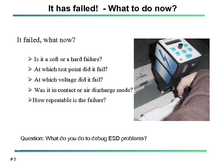
It has failed! - What to do now? It failed, what now? Ø Is it a soft or a hard failure? Ø At which test point did it fail? Ø At which voltage did it fail? Ø Was it in contact or air discharge mode? ØHow repeatable is the failure? Question: What do you do to debug ESD problems? #5
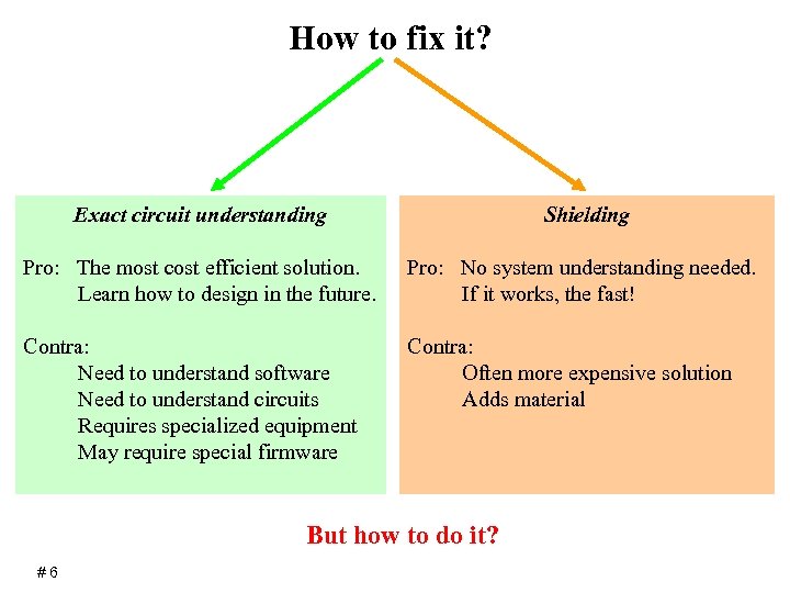
How to fix it? Exact circuit understanding Shielding Pro: The most cost efficient solution. Learn how to design in the future. Pro: No system understanding needed. If it works, the fast! Contra: Need to understand software Need to understand circuits Requires specialized equipment May require special firmware Contra: Often more expensive solution Adds material But how to do it? #6
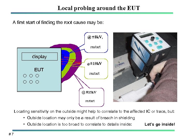
Local probing around the EUT A first start of finding the root cause may be: @ 8 k. V, restart display EUT 20 mm 50 mm 200 mm @ 10 k. V restart @ 15 k. V restart Locating sensitivity on the outside might help to correlate to the affected IC or trace, but: • Outside location may only be a result of breach in shielding • Outside location is too broad to correlate to details inside: #7 Let’s go inside!
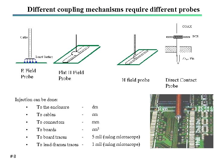
Different coupling mechanisms require different probes Injection can be done: • - dm • To cables - cm • To connectors - mm • To boards - cm 2 • To board traces - 5 mil (using microscope) • #8 To the enclosure To lead-frames traces - 1 mil (using microscope)
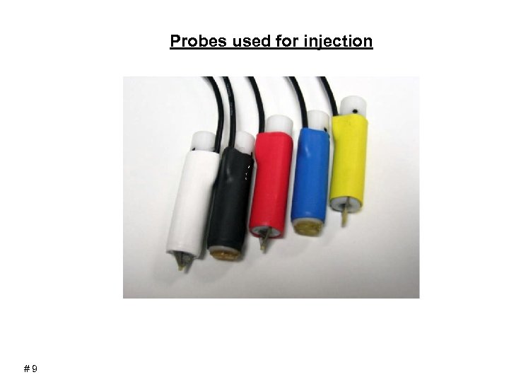
Probes used for injection #9
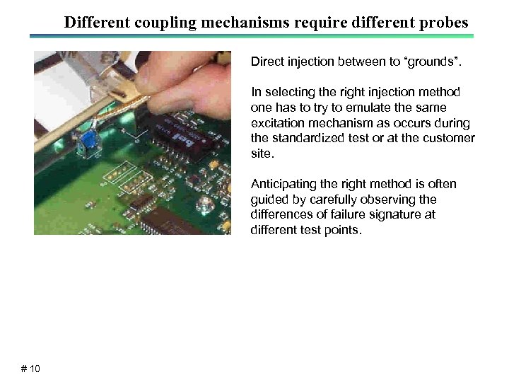
Different coupling mechanisms require different probes Direct injection between to “grounds”. In selecting the right injection method one has to try to emulate the same excitation mechanism as occurs during the standardized test or at the customer site. Anticipating the right method is often guided by carefully observing the differences of failure signature at different test points. # 10
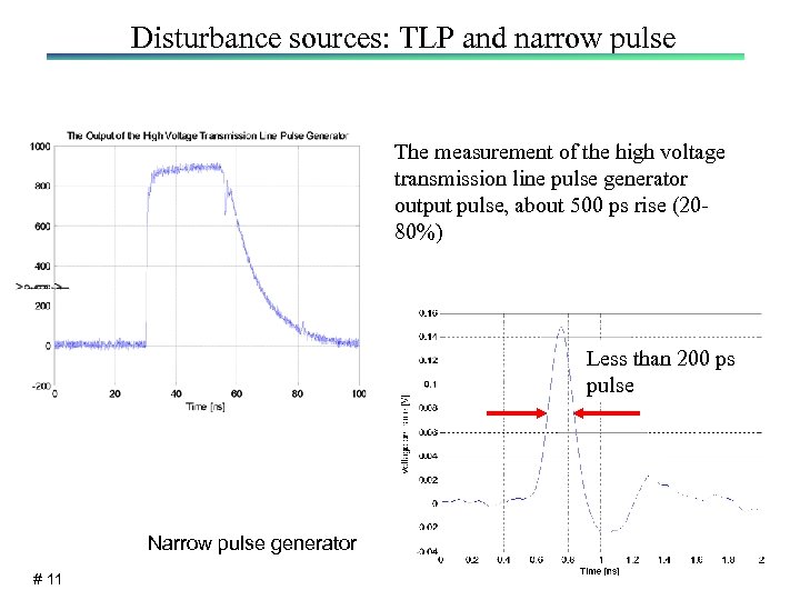
Disturbance sources: TLP and narrow pulse The measurement of the high voltage transmission line pulse generator output pulse, about 500 ps rise (2080%) Less than 200 ps pulse Narrow pulse generator # 11
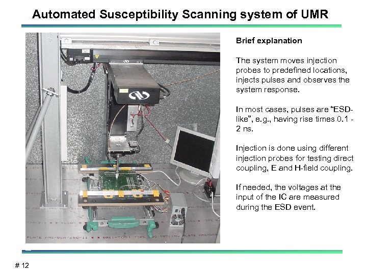
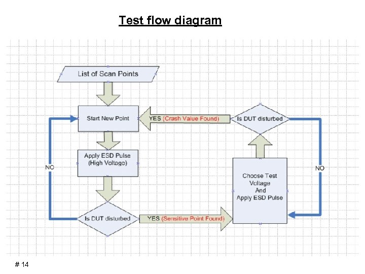
Automated Susceptibility Scanning system of UMR Brief explanation The system moves injection probes to predefined locations, injects pulses and observes the system response. In most cases, pulses are “ESDlike”, e. g. , having rise times 0. 1 2 ns. Injection is done using different injection probes for testing direct coupling, E and H-field coupling. If needed, the voltages at the input of the IC are measured during the ESD event. # 12
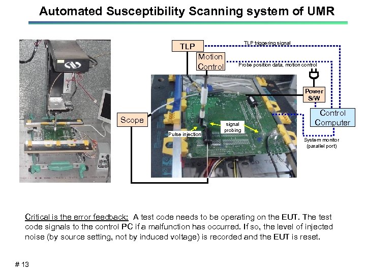
Automated Susceptibility Scanning system of UMR TLP triggering signal TLP Motion Control Probe position data, motion control Power S/W Scope Pulse injection signal probing Control Computer System monitor (parallel port) Critical is the error feedback: A test code needs to be operating on the EUT. The test code signals to the control PC if a malfunction has occurred. If so, the level of injected noise (by source setting, not by induced voltage) is recorded and the EUT is reset. # 13
Test flow diagram # 14
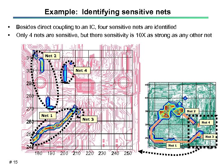
Example: Identifying sensitive nets • • Besides direct coupling to an IC, four sensitive nets are identified Only 4 nets are sensitive, but there sensitivity is 10 X as strong as any other net Net 2 310 Net 4 300 290 450 280 400 270 Net 3 260 Net 4 300 250 Net 3 250 240 50 180 # 15 Net 2 350 Net 1 190 200 210 220 230 240 250 Net 1 100 150 200 250
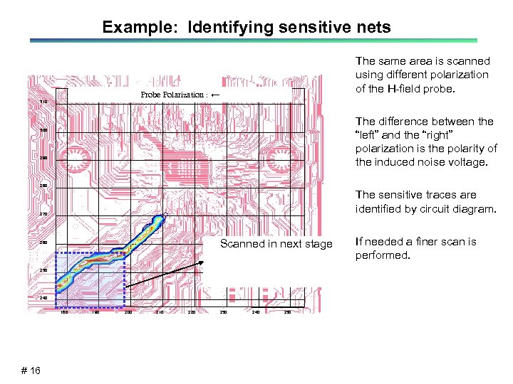
Example: Identifying sensitive nets The same area is scanned using different polarization of the H-field probe. Probe Polarization : ← 310 The difference between the “left” and the “right” polarization is the polarity of the induced noise voltage. 300 290 280 The sensitive traces are identified by circuit diagram. 270 Scanned in next stage 260 250 240 180 # 16 190 200 210 220 230 240 250 If needed a finer scan is performed.
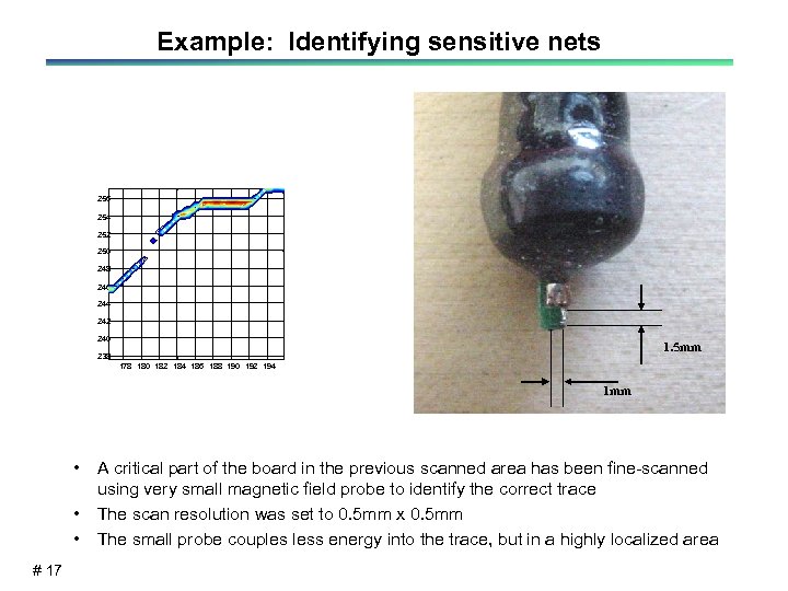
Example: Identifying sensitive nets 256 254 252 250 248 246 244 242 240 1. 5 mm 238 178 180 182 184 186 188 190 192 194 1 mm • A critical part of the board in the previous scanned area has been fine-scanned using very small magnetic field probe to identify the correct trace • The scan resolution was set to 0. 5 mm x 0. 5 mm • The small probe couples less energy into the trace, but in a highly localized area # 17
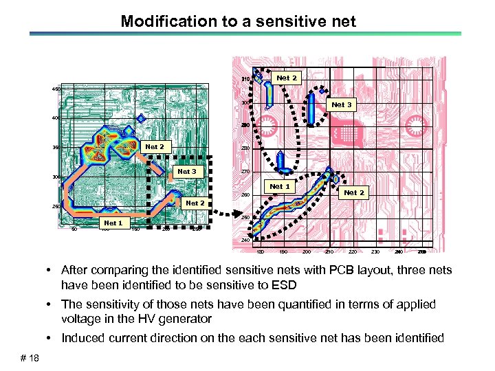
Modification to a sensitive net Net 2 310 450 300 Net 3 400 290 Net 2 350 280 Net 3 300 270 Net 1 Net 2 260 Net 2 250 50 Net 1 100 250 150 200 250 240 180 190 200 210 220 230 240 250 • After comparing the identified sensitive nets with PCB layout, three nets have been identified to be sensitive to ESD • The sensitivity of those nets have been quantified in terms of applied voltage in the HV generator • Induced current direction on the each sensitive net has been identified # 18
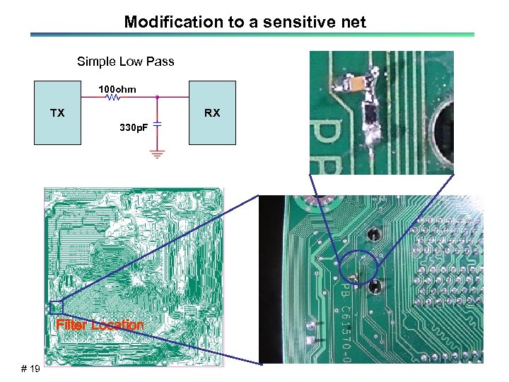
Modification to a sensitive net Simple Low Pass 100 ohm TX RX 330 p. F Filter Location # 19
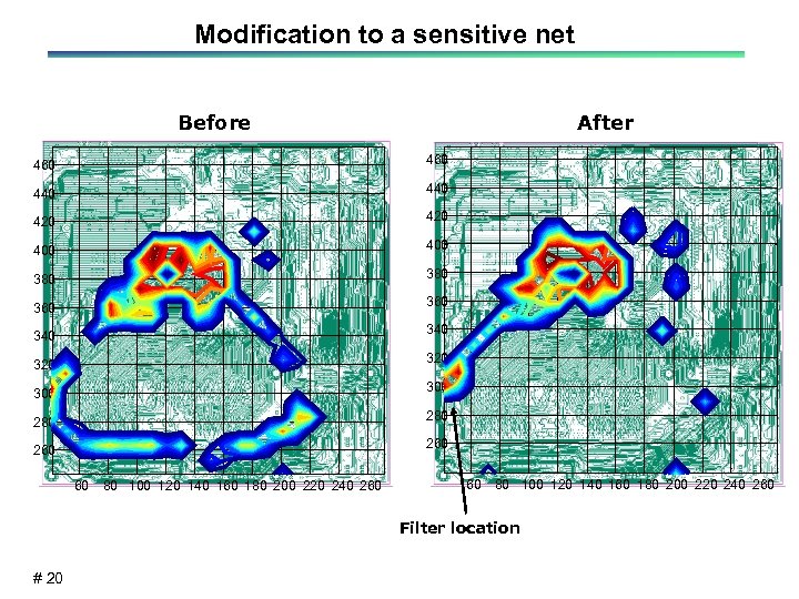
Modification to a sensitive net Before After 460 440 420 400 380 360 340 320 300 280 260 60 80 100 120 140 160 180 200 220 240 260 Filter location # 20
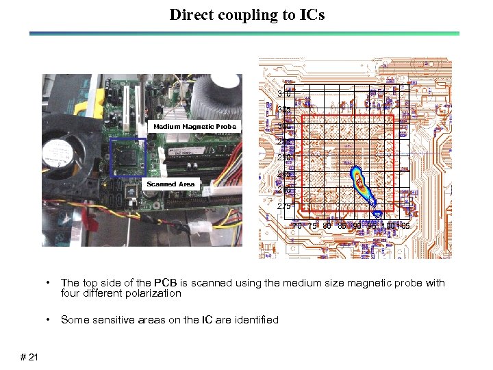
Direct coupling to ICs 310 305 Medium Magnetic Probe 300 295 290 285 Scanned Area 280 275 70 75 80 85 90 95 100 105 • The top side of the PCB is scanned using the medium size magnetic probe with four different polarization • Some sensitive areas on the IC are identified # 21
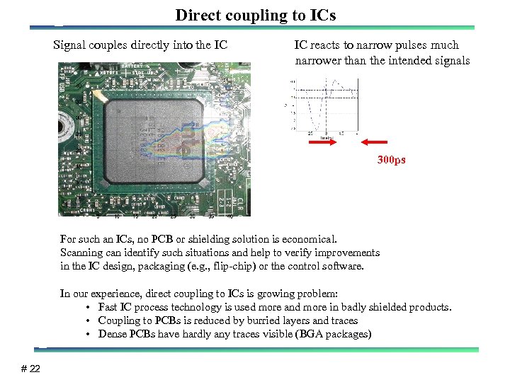
Direct coupling to ICs Signal couples directly into the IC IC reacts to narrow pulses much narrower than the intended signals 300 ps For such an ICs, no PCB or shielding solution is economical. Scanning can identify such situations and help to verify improvements in the IC design, packaging (e. g. , flip-chip) or the control software. In our experience, direct coupling to ICs is growing problem: • Fast IC process technology is used more and more in badly shielded products. • Coupling to PCBs is reduced by burried layers and traces • Dense PCBs have hardly any traces visible (BGA packages) # 22
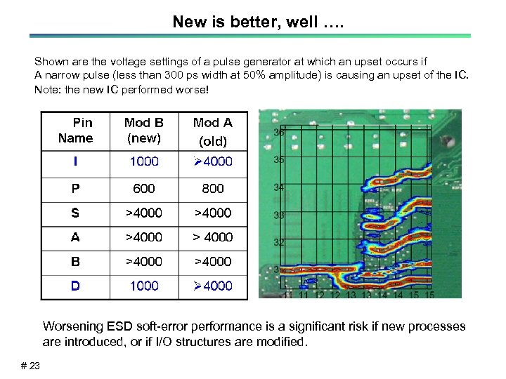
New is better, well …. Shown are the voltage settings of a pulse generator at which an upset occurs if A narrow pulse (less than 300 ps width at 50% amplitude) is causing an upset of the IC. Note: the new IC performed worse! Worsening ESD soft-error performance is a significant risk if new processes are introduced, or if I/O structures are modified. # 23
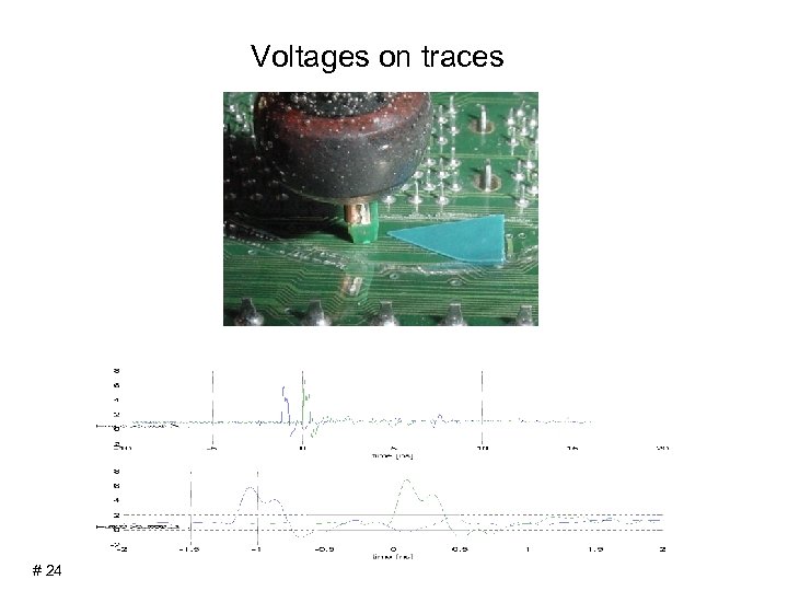
Voltages on traces # 24
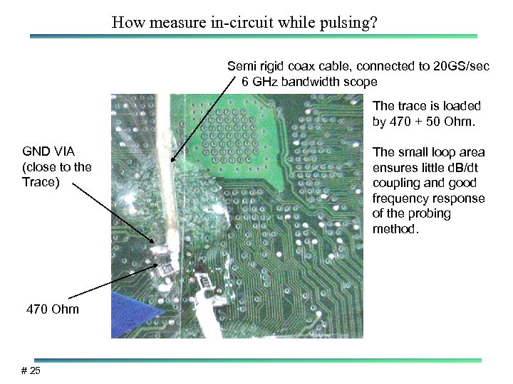
How measure in-circuit while pulsing? Semi rigid coax cable, connected to 20 GS/sec 6 GHz bandwidth scope The trace is loaded by 470 + 50 Ohm. GND VIA (close to the Trace) 470 Ohm # 25 The small loop area ensures little d. B/dt coupling and good frequency response of the probing method.
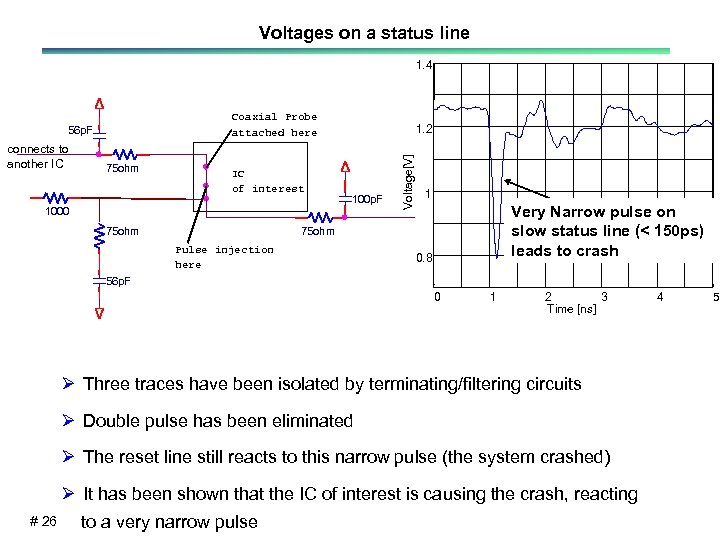
Voltages on a status line 1. 4 Coaxial Probe attached here connects to another IC 75 ohm IC of interest Inner layer trace 1000 75 ohm 1. 2 100 p. F 75 ohm Pulse injection here Voltage[V] 56 p. F 1 Very Narrow pulse on slow status line (< 150 ps) leads to crash connects to another IC 0. 8 56 p. F 0 1 2 3 Time [ns] Ø Three traces have been isolated by terminating/filtering circuits Ø Double pulse has been eliminated Ø The reset line still reacts to this narrow pulse (the system crashed) Ø It has been shown that the IC of interest is causing the crash, reacting # 26 to a very narrow pulse 4 5
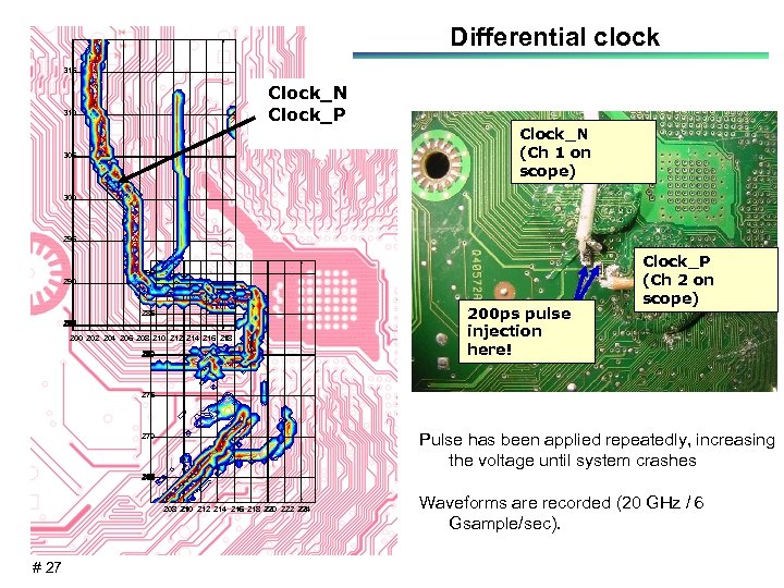
Differential clock 315 Clock_N Clock_P 310 305 Clock_N (Ch 1 on scope) 300 295 290 285 200 202 204 206 208 210 212 214 216 218 280 200 ps pulse injection here! Clock_P (Ch 2 on scope) 275 Pulse has been applied repeatedly, increasing the voltage until system crashes 270 265 208 210 212 214 216 218 220 222 224 # 27 Waveforms are recorded (20 GHz / 6 Gsample/sec).
![Voltage on trace [V] ESD Event on differential clock -5 V, on DP, crashed Voltage on trace [V] ESD Event on differential clock -5 V, on DP, crashed](https://present5.com/presentation/04f6219e594053ac3b60bee3af65e91a/image-28.jpg)
Voltage on trace [V] ESD Event on differential clock -5 V, on DP, crashed - 2 0. 8 0. 4 0 0 10 Voltage difference Voltage[V] 1 Very sensitive to noise during the transition # 28 crash 0 -1 20 0 10 Time [ns] 20
![1 0 0 4 Voltage[V] 1 16 20 -8 V, on DP, Crashed - 1 0 0 4 Voltage[V] 1 16 20 -8 V, on DP, Crashed -](https://present5.com/presentation/04f6219e594053ac3b60bee3af65e91a/image-29.jpg)
1 0 0 4 Voltage[V] 1 16 20 -8 V, on DP, Crashed - 2 1 crash 0 0 4 1 0 -1 8 12 Voltage difference Voltage on trace [V] 20 V, on DP, Not crashed - 1 2 Voltage[V] Voltage on trace [V] ESD Event on differential clock No crash! 0 4 8 12 Time [ns] 16 20 8 12 Voltage difference 16 Crash threshold : approx. 0. 2 V 0 -1 0 4 8 12 Time [ns] 16 Crash threshold : approx. 0. 2 V Clock_P + Clock_N # 29 20 - Differential input has an offset 20
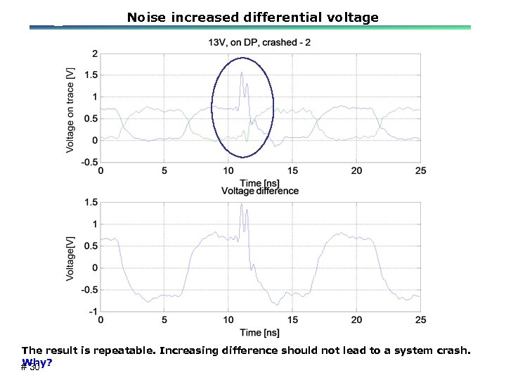
Noise increased differential voltage The result is repeatable. Increasing difference should not lead to a system crash. Why? # 30
![Voltage on trace [V] ESD on differential clock – Common Mode disturbance 2 No Voltage on trace [V] ESD on differential clock – Common Mode disturbance 2 No](https://present5.com/presentation/04f6219e594053ac3b60bee3af65e91a/image-31.jpg)
Voltage on trace [V] ESD on differential clock – Common Mode disturbance 2 No crash 1 0 0 4 Voltage[V] 12 16 20 Voltage difference 1 # 31 8 0 -1 0 4 8 Time [ns] 12 If the common mode voltage is relatively low, the differential input will suppress the common mode signal. 2 x 330
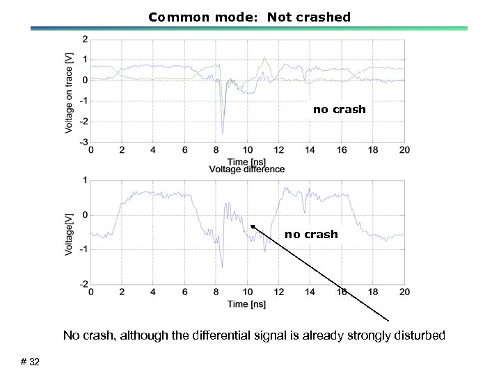
Common mode: Not crashed no crash No crash, although the differential signal is already strongly disturbed # 32
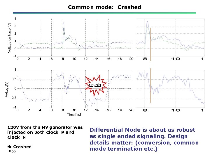
Common mode: Crashed crash 120 V from the HV generator was injected on both Clock_P and Clock_N Crashed # 33 Differential Mode is about as robust as single ended signaling. Design details matter: (conversion, common mode termination etc. )
How an IC can react to pulses • Voltage surpasses threshold for a sufficiently long time • Linear network, bond wire inductance and input capacitance, ring or peak the pulse, leading to a softerror. • Voltage triggers non-linear effect on the input buffer • Voltage causes ESD protection to forward bias, causes substrate injection or internal power fluctuations, leading to crash • Current leads to latch-up, or latch-up like situation. # 34
Open Questions Ø Immunity problems caused by global coupling vs. local coupling to one trace. Ø Correlation system level – board level. Ø IC level immunity test methods and robustness guidelines for IC design are not well developed yet. Ø IC level immunity standards. Ø Software for improving immunity. Ø Latch-up and ESD protection circuit recovery, how many of the observed soft errors are caused by latch-up? # 35
Conclusion Ø Using local injection the disturbed traced can be identified. Ø The sensitivity of I/O ports can be quantified. Ø These data can be used to analyze the function of circuits designed to reduce ESD sensitivity. Ø In-circuit measurements can be done while doing local injection, as the amount of common mode signal is vastly reduced. This is a developing field, many questions are still out there, just waiting to be solved. # 36
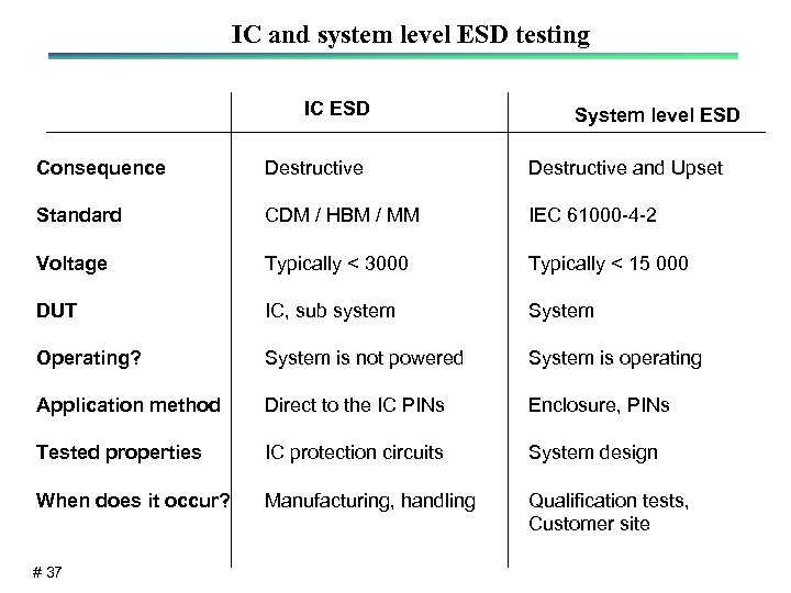
IC and system level ESD testing IC ESD System level ESD Consequence Destructive and Upset Standard CDM / HBM / MM IEC 61000 -4 -2 Voltage Typically < 3000 Typically < 15 000 DUT IC, sub system System Operating? System is not powered System is operating Application method Direct to the IC PINs Enclosure, PINs Tested properties IC protection circuits System design When does it occur? Manufacturing, handling Qualification tests, Customer site # 37
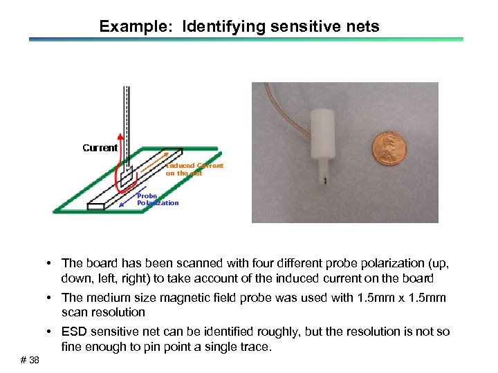
Example: Identifying sensitive nets Induced Current on the net Probe Polarization • The board has been scanned with four different probe polarization (up, down, left, right) to take account of the induced current on the board • The medium size magnetic field probe was used with 1. 5 mm x 1. 5 mm scan resolution • ESD sensitive net can be identified roughly, but the resolution is not so fine enough to pin point a single trace. # 38
04f6219e594053ac3b60bee3af65e91a.ppt