ba5ce09981e1eb4564bbcbde3ff72a19.ppt
- Количество слайдов: 61

Finding and Sharing Brick Walls CANDE September 22, 2001 Andrew B. Kahng, UCSD CSE & ECE Departments email: abk@ucsd. edu URL: http: //vlsicad. ucsd. edu Andrew Kahng – September 2001
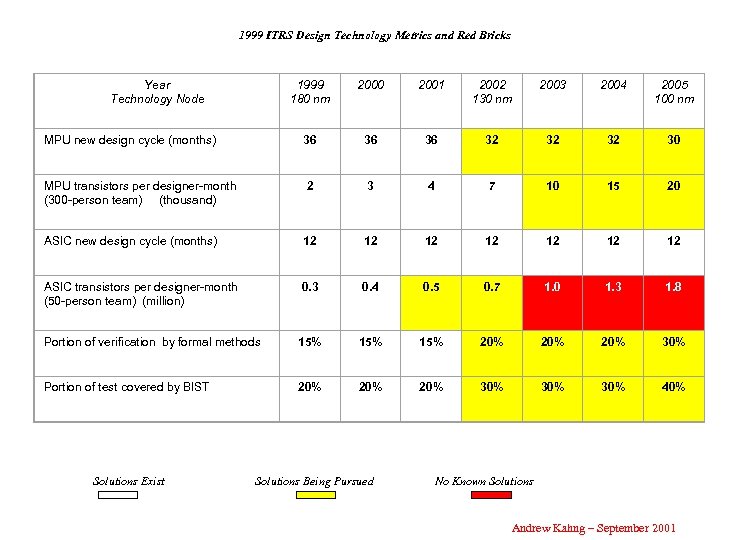
1999 ITRS Design Technology Metrics and Red Bricks Year Technology Node 1999 180 nm 2000 2001 2002 130 nm 2003 2004 2005 100 nm MPU new design cycle (months) 36 36 36 32 32 32 30 MPU transistors per designer-month (300 -person team) (thousand) 2 3 4 7 10 15 20 ASIC new design cycle (months) 12 12 ASIC transistors per designer-month (50 -person team) (million) 0. 3 0. 4 0. 5 0. 7 1. 0 1. 3 1. 8 Portion of verification by formal methods 15% 15% 20% 20% 30% Portion of test covered by BIST 20% 20% 30% 30% 40% Solutions Exist Solutions Being Pursued No Known Solutions Andrew Kahng – September 2001

Hold These Thoughts… • ITRS is created by SIA companies and top semi/system houses worldwide – all star customers • EDA has one chapter out of 12 • EDA is just another part of SISA (semiconductor industry supplier association) • EDA is small: 6000 R&D worldwide, $4 B market • Hold this thought: Dataquest 3. 9% annual growth in tools $ spent per designer; integration costs > tool costs • Hold this thought: “small industry with poor perceived ROI will stay small” = vicious cycle • Hold this thought: How do we turn a vicious cycle into a virtuous cycle? Andrew Kahng – September 2001

Six Riffs • Riff #1: ITRS acceleration, silicon technology, and system drivers • Riff #2: A big picture on red bricks • Riff #3: A Dark Riff on D and DT productivity • Riff #4: On the design-manufacturing handoff • Riff #5: On cost, variability and value • Riff #6: It’s lunchtime Andrew Kahng – September 2001

Riff #1: ITRS Acceleration, Silicon Technology, and System Drivers Andrew Kahng – September 2001

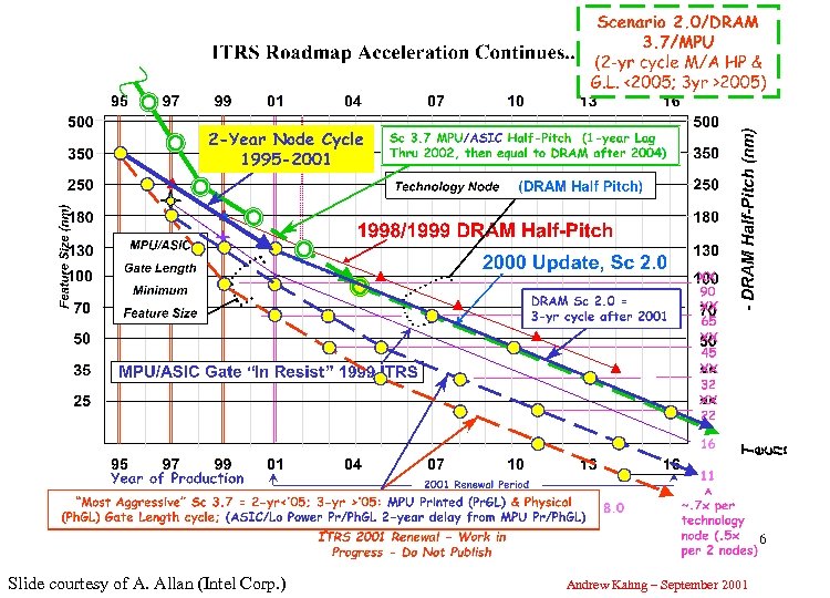
Roadmap Acceleration Since 2000 • Major accelerations continue – E. g. , 90 nm node is in 2004, with physical gate length at 45 nm • MPU/ASIC half-pitch were separate, now unified – ASIC is at the same process node as MPU • 2 -year cycles b/w MPU/ASIC generations through 2004 – Node = 0. 7 x multiplier of half-pitch or minimum feature size, generally allowing 2 x the transistors on the same size die – “Normal” pace = 3 -year cycle • MPU/ASIC half-pitch converges w/DRAM HP in 2004 – Previous ITRS (2000): convergence predicted for 2015 – Extremely aggressive scaling for density, cost improvement and competitive positioning Andrew Kahng – September 2001
Slide courtesy of A. Allan (Intel Corp. ) Andrew Kahng – September 2001

System Drivers • Define IC products that drive mfg, design technologies • ORTCs + SDs = “consistent framework for tech requirements” • Four system drivers – – MPU – traditional processor core SOC (focus on “ASIC-LP”, + high-pins, high-signaling network driver) AM/S – four basic circuits and FOMs DRAM • Each driver section • • Nature, evolution, formal definition of this driver What market forces apply to this driver ? What technology elements (process, device, design) does this drive? Key figures of merit, and roadmap Andrew Kahng – September 2001

MPU Driver • Old MPU model – 3 flavors • New MPU model - 2 flavors • Cost-performance at production (CP) – 140 mm 2 die, “desktop” • High-performance at production (HP) – 310 mm 2 die, “server” • Both have multiple cores (“helper engines”), on-board L 3 cache, … – Multi-cores == more dedicated, less general-purpose logic; driven by power and reuse considerations; reflect convergence of MPU and SOC • Doubling of transistor counts is each per each node, NOT per each 18 months • Clock frequencies stop doubling with each node Andrew Kahng – September 2001

Example Supporting Analyses (MPU) • Diminishing returns – Pollack’s Rule: In a given process technology, new microarchitecture takes 2 -3 x area of previous generation one, and provides only 50% more performance – Corroboration: SPECint/MHz, SPECfp/MHz, SPECint/Watt all decreasing • Power knob running out – Speed == Power – Large switching currents, large power surges on wakeup, IR drop control issues all limited by A&P roadmap (e. g. , improvement in bump pitch, package power) • Power management: 2500% improvement needed by 2016 • Speed knob running out (new clock frequency model) – Historically, 2 x clock frequency every node • 1. 4 x/node from device scaling but running into tox, other limits (PIDS) • 1. 4 x/node from fewer logic stages (from 40 -100 down to around 14 FO 4 INV delays) – Clocks cannot be generated with period < 6 -8 FO 4 INV delays – Pipelining overhead (1 -1. 5 FO 4 INV delay for pulse-mode latch, 2 -3 for FF) – Around 16 FO 4 INV delays is limit for clock period in core (L 1 $ access, 64 b add) – Cannot continue 2 x frequency per node trend in ITRS Andrew Kahng – September 2001

SOC-LP Driver • Power gap – Must reduce dynamic and static power to avoid “zero logic content limit” – Hits low-power SOC before hits MPU – SOC degree of freedom: low-power (not high-perf) process • SOC-LP model drives ASIC-LP (PIDS) device model – Lgate lags high-performance devices by 2 years, but layout density same – Accompanying device parameter changes • • Vth higher, Vdd higher Ig, Ioff starts at 100 p. A/um (L(Operating)P), 1 p. A/um (L(STandby)P) Tox higher Slower devices (larger CV/I) – Even with four LP device flavors, Design still faces large static power management challenge, and must handle multi (Vt, tox, Vdd) • SOC-LP driver: low-power PDA – Composition: CPU cores, embedded cores, SRAM/e. DRAM – Roadmap for IO bandwidth, processing power, GOPS/m. W efficiency – Die size grows at 20% per node Andrew Kahng – September 2001
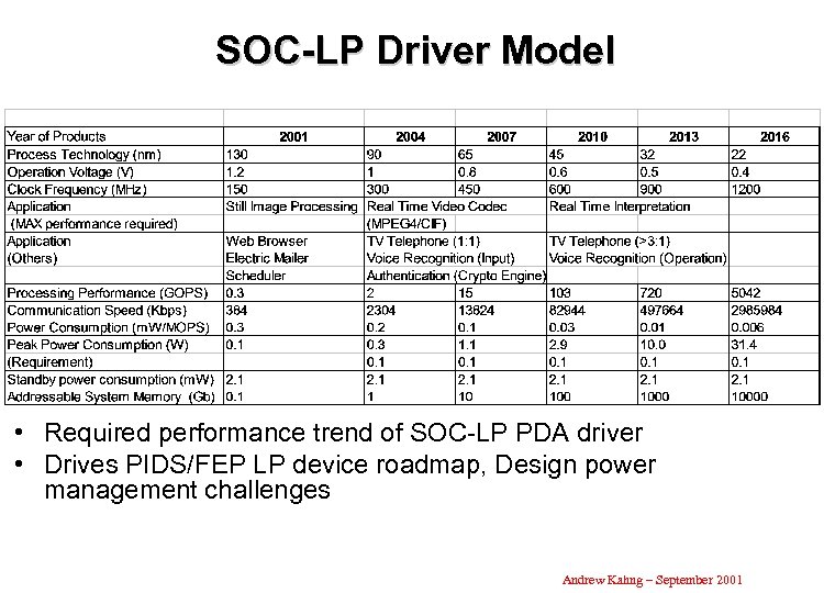
SOC-LP Driver Model • Required performance trend of SOC-LP PDA driver • Drives PIDS/FEP LP device roadmap, Design power management challenges Andrew Kahng – September 2001
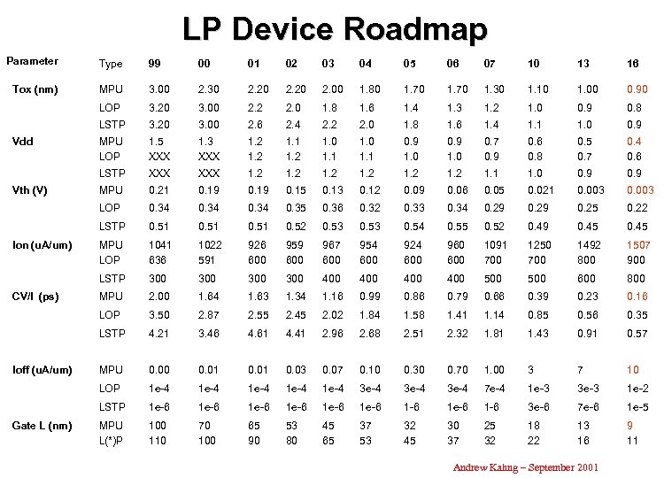
LP Device Roadmap Parameter Type 99 00 01 02 03 04 05 06 07 10 13 16 Tox (nm) MPU 3. 00 2. 30 2. 20 2. 00 1. 80 1. 70 1. 30 1. 10 1. 00 0. 90 LOP 3. 20 3. 00 2. 2 2. 0 1. 8 1. 6 1. 4 1. 3 1. 2 1. 0 0. 9 0. 8 LSTP 3. 20 3. 00 2. 6 2. 4 2. 2 2. 0 1. 8 1. 6 1. 4 1. 1 1. 0 0. 9 Vdd MPU LOP 1. 5 XXX 1. 3 XXX 1. 2 1. 1 1. 2 1. 0 1. 1 0. 9 1. 0 0. 7 0. 9 0. 6 0. 8 0. 5 0. 7 0. 4 0. 6 LSTP XXX 1. 2 1. 1 1. 0 0. 9 Vth (V) MPU 0. 21 0. 19 0. 15 0. 13 0. 12 0. 09 0. 06 0. 05 0. 021 0. 003 LOP 0. 34 0. 35 0. 36 0. 32 0. 33 0. 34 0. 29 0. 25 0. 22 LSTP 0. 51 0. 52 0. 53 0. 54 0. 55 0. 52 0. 49 0. 45 Ion (u. A/um) MPU LOP 1041 636 1022 591 926 600 959 600 967 600 954 600 924 600 960 600 1091 700 1250 700 1492 800 1507 900 LSTP 300 300 400 400 500 600 800 CV/I (ps) MPU 2. 00 1. 64 1. 63 1. 34 1. 16 0. 99 0. 86 0. 79 0. 66 0. 39 0. 23 0. 16 LOP 3. 50 2. 87 2. 55 2. 45 2. 02 1. 84 1. 58 1. 41 1. 14 0. 85 0. 56 0. 35 LSTP 4. 21 3. 46 4. 61 4. 41 2. 96 2. 68 2. 51 2. 32 1. 81 1. 43 0. 91 0. 57 Ioff (u. A/um) MPU 0. 00 0. 01 0. 03 0. 07 0. 10 0. 30 0. 70 1. 00 3 7 10 LOP 1 e-4 1 e-4 3 e-4 7 e-4 1 e-3 3 e-3 1 e-2 LSTP 1 e-6 1 e-6 1 -6 3 e-6 7 e-6 1 e-5 Gate L (nm) MPU L(*)P 100 110 70 100 65 90 53 80 45 65 37 53 32 45 30 37 25 32 18 22 13 16 9 11 Andrew Kahng – September 2001
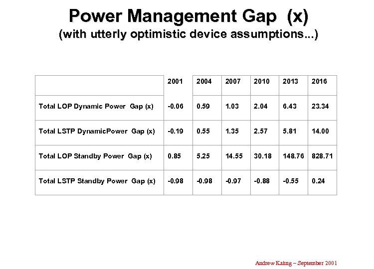
Power Management Gap (x) (with utterly optimistic device assumptions. . . ) 2001 2004 2007 2010 2013 2016 Total LOP Dynamic Power Gap (x) -0. 06 0. 59 1. 03 2. 04 6. 43 23. 34 Total LSTP Dynamic. Power Gap (x) -0. 19 0. 55 1. 35 2. 57 5. 81 14. 00 Total LOP Standby Power Gap (x) 0. 85 5. 25 14. 55 30. 18 148. 76 828. 71 Total LSTP Standby Power Gap (x) -0. 98 -0. 97 -0. 88 -0. 55 0. 24 Andrew Kahng – September 2001

Riff #2: The Big Picture on Red Bricks Andrew Kahng – September 2001
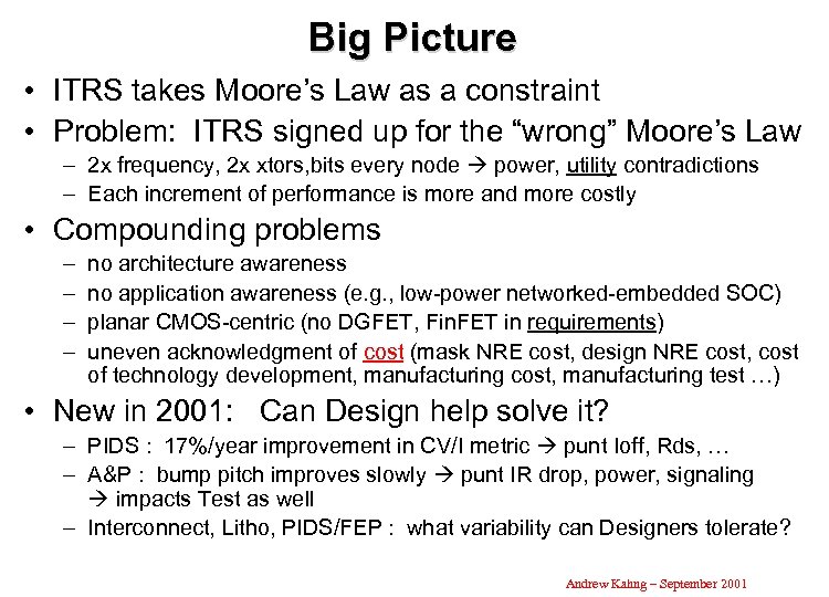
Big Picture • ITRS takes Moore’s Law as a constraint • Problem: ITRS signed up for the “wrong” Moore’s Law – 2 x frequency, 2 x xtors, bits every node power, utility contradictions – Each increment of performance is more and more costly • Compounding problems – – no architecture awareness no application awareness (e. g. , low-power networked-embedded SOC) planar CMOS-centric (no DGFET, Fin. FET in requirements) uneven acknowledgment of cost (mask NRE cost, design NRE cost, cost of technology development, manufacturing cost, manufacturing test …) • New in 2001: Can Design help solve it? – PIDS : 17%/year improvement in CV/I metric punt Ioff, Rds, … – A&P : bump pitch improves slowly punt IR drop, power, signaling impacts Test as well – Interconnect, Litho, PIDS/FEP : what variability can Designers tolerate? Andrew Kahng – September 2001

DT Integration With Other Technologies • Problem: Design has always been “metric-free” – Metric “red brick wall” requirement for R&D investment • EDA Goal 1: show red bricks in Design Technology • EDA Goal 2: shift red bricks from other supporting technologies – e. g. , lithography CD variability requirement solved by new Design techniques that can better handle variability – e. g. , mask data volume requirement solved by Design/Mfg interfaces and flows that pass functional requirements, verification knowledge to mask writing and inspection – e. g. , Simplex “X initiative” as much impact as copper ? • It’s an ROI issue !!! – Need metrics of design cost, design quality/value DT ROI – Need serious validation/participation from EDA community before we can expect help from system, ASIC companies Andrew Kahng – September 2001
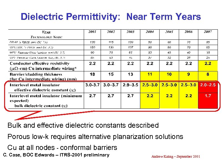
Dielectric Permittivity: Near Term Years Bulk and effective dielectric constants described Porous low-k requires alternative planarization solutions Cu at all nodes - conformal barriers C. Case, BOC Edwards – ITRS-2001 preliminary Andrew Kahng – September 2001
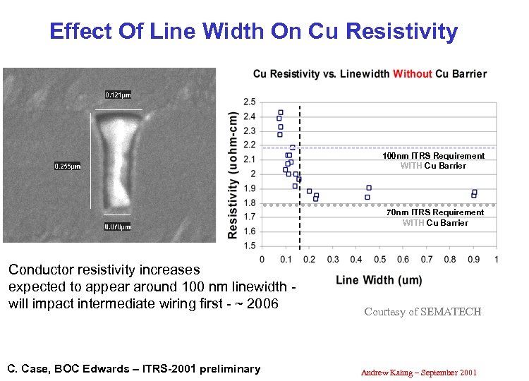
Effect Of Line Width On Cu Resistivity 100 nm ITRS Requirement WITH Cu Barrier 70 nm ITRS Requirement WITH Cu Barrier Conductor resistivity increases expected to appear around 100 nm linewidth will impact intermediate wiring first - ~ 2006 C. Case, BOC Edwards – ITRS-2001 preliminary Courtesy of SEMATECH Andrew Kahng – September 2001

Device Roadmap Changes • Process Integration, Devices and Structures (PIDS) • CV/I delay metric: historically decreases by 17%/year – Since frequency improvement from shorter pipelines no longer available, perhaps we do need to keep scaling CV/I … – Bottom line: PIDS is running up against limits of planar CMOS, and is shifting at least some of the pain to “design/architecture improvements” • Continuing CV/I trend necessitates huge growth in Ioff • Subthreshold Ioff at room temperature increases from 0. 01 u. A/um in 2001 to 10 u. A/um at end of ITRS (22 nm node) • Ioff increases by at least order of magnitude at ~100 deg C operating temps (40 x difference between 25 deg C and 125 deg C) • Static power becomes a huge problem: multi-Vt, multi-Vdd, substrate biasing, constant-throughput power minimization, etc. must be coherently and simultaneously applied/optimized by automatic tools • Also necessitates aggressive reduction in tox • Physical tox thickness hovers at < 1. 4 nm (down to 1. 0 nm) starting in 2001, even assuming arrival of high-k gate dielectrics starting in 2004 • Implies huge variability mitigation challenges for Design Technology: “ 10%” < one monolayer… Andrew Kahng – September 2001

Assembly/Packaging Roadmap • MPU pad counts flat from 2001 -2005; chip current draw increases 64% • Effective bump pitch roughly constant at 350 mm – Bump/pad counts scale with chip area only, do not increase with technology demands (IR drop, L*di/dt) – metal resources needed to control <10% IR drop skyrocket since Ichip and wiring resistance increase challenge for DT – Later technologies (30 -40 nm) also have too few bumps to carry maximum current draw (e. g. , 1250 Vdd pads at 30 nm with bump pitch of 250 mm can each carry 150 m. A 187. 5 A max capability but Ichip/Vdd > 300 A • A&P Rationale: cost control (puts pain onto Design) • Design Rationalization: must add power constraints – ITRS 2001 will have strong power-constrained focus • Cost of liquid cooling, refrigeration, etc. impractical anyway (? ? ? ) • 30 -50 W/cm 2 limit forced-air cooling with fins • MPU power dissipation capped at 200 W; MPU chip area held constant (more area can’t be used well within 150 W power budget) Andrew Kahng – September 2001

Design Technology and the ITRS • Cost = biggest hole in ITRS and in DT • Manufacturing cost, NRE cost (design, mask, …), technology development cost (= who should have/solve red brick walls? ) • Challenges for DT (with respect to ITRS) • • Circuit/layout optimizations in the face of manufacturing variability System cost-driven design technology Holistic analysis, management of power (both dynamic and static) Circuit- and methodology-level IP: global signaling and synchronization, off-chip IO; power delivery and management • Metrics, needs roadmap for quality/cost/ROI of design and design process • Verification and test (else cost of mfg test soon exceeds cost of mfg) • Software Andrew Kahng – September 2001

Riff #3: A Dark Riff on D and DT Productivity Andrew Kahng – September 2001
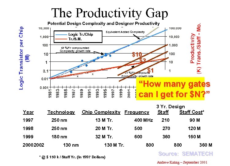
The Productivity Gap Potential Design Complexity and Designer Productivity Logic Tr. /Chip Tr. /S. M. Equivalent Added Complexity 68 %/Yr compounded Complexity growth rate $10 $3 $1 21 %/Yr compound Productivity growth rate “How many gates can I get for $N? ” 3 Yr. Design Year Technology Chip Complexity Frequency Staff Cost* 1997 250 nm 13 M Tr. 400 MHz 210 90 M 1998 250 nm 20 M Tr. 500 270 120 M 1999 180 nm 32 M Tr. 600 360 160 M 2000 2002 130 nm 130 M Tr. 800 360 M * @ $ 150 k / Staff Yr. (In 1997 Dollars) Source: SEMATECH Andrew Kahng – September 2001
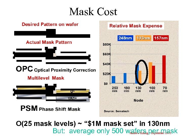
Mask Cost O(25 mask levels) ~ “$1 M mask set” in 130 nm But: average only 500 wafers per mask Andrew Kahng – September 2001

“Keep the Fabs Full” • Design technology must keep manufacturing facilities fully utilized with: – high-volume parts – high-margin parts • Foundry capital cost > $2 B – How much value of new designs is needed to fill the fab ? ? ? Andrew Kahng – September 2001
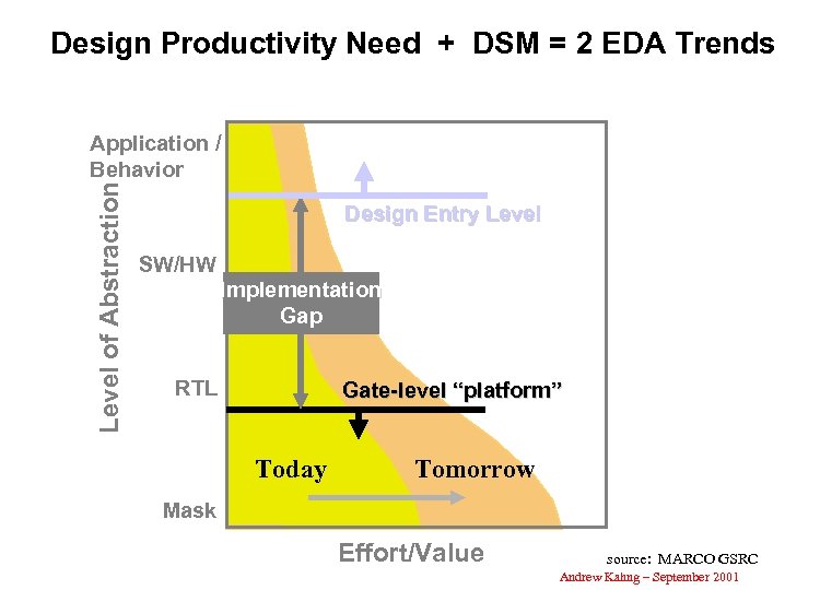
Design Productivity Need + DSM = 2 EDA Trends Level of Abstraction Application / Behavior Design Entry Level SW/HW Implementation Gap RTL Gate-level “platform” Today Tomorrow Mask Effort/Value source: MARCO GSRC Andrew Kahng – September 2001
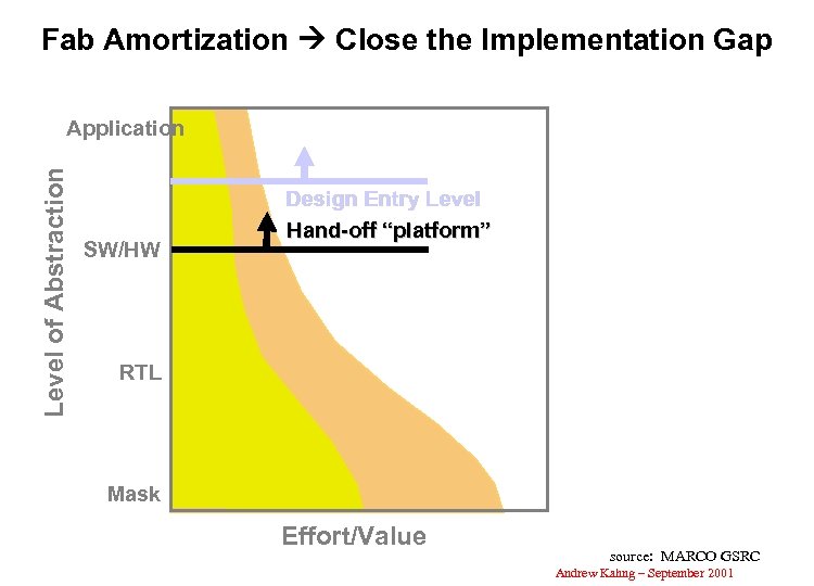
Fab Amortization Close the Implementation Gap Level of Abstraction Application SW/HW Design Entry Level Hand-off “platform” RTL Mask Effort/Value source: MARCO GSRC Andrew Kahng – September 2001

Design Productivity Gap Low-Value Designs? Percent of die area that must be occupied by memory t maintain SOC design productivity Source = Japanese system-LSI industry Andrew Kahng – September 2001
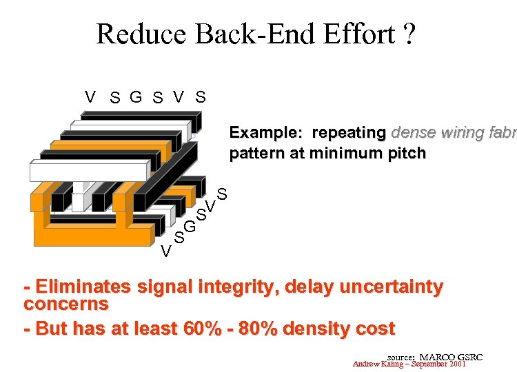
Reduce Back-End Effort ? V S G S V S Example: repeating dense wiring fabri dense wiring fabr pattern at minimum pitch V S G S V SV G S S - Eliminates signal integrity, delay uncertainty concerns - But has at least 60% - 80% density cost source: MARCO GSRC Andrew Kahng – September 2001
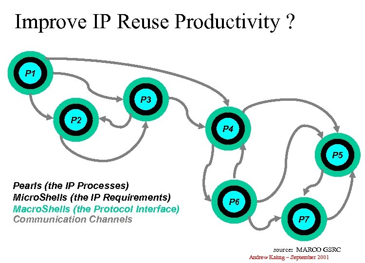
Improve IP Reuse Productivity ? P 1 P 3 P 2 P 4 P 5 Pearls (the IP Processes) Micro. Shells (the IP Requirements) Macro. Shells (the Protocol Interface) Communication Channels P 6 P 7 source: MARCO GSRC Andrew Kahng – September 2001

QUALITY Problem : > 1000 x Energy-Flexibility Gap Energy Efficiency MOPS/m. W (or MIPS/m. W) 1000 10 1 Dedicated HW 100 -200 MOPS/m. W Reconfigurable Processor/Logic 10 -50 MOPS/m. W 1 V DSP 3 MOPS/m. W ASIPs DSPs Embedded m. Processors LP ARM 0. 5 -2 MIPS/m. W 0. 1 Flexibility (Coverage) Source: Prof. Jan Rabaey, UC Berkeley Andrew Kahng – September 2001

“Keep the Fabs Full” • Design technology must keep manufacturing facilities fully utilized with: – high-volume parts – high-margin parts • What happens when design technology “fails” ? – not enough high-value designs – the semiconductor industry will find a “workaround” • reconfigurable logic • platform-based design • extract value somewhere other than silicon differentiation Andrew Kahng – September 2001

Dark Riff Conclusions • Design productivity gap threatens design quality design starts, business models at risk – TAT achieved at cost of QOR – low QOR low silicon value – electronics industry chooses reprogrammable, platform-based “workarounds” • We need to understand cost and quality/value Andrew Kahng – September 2001

Two CANDE-01 Non-Predictions • Jim Sproch, Synopsys: – “Summary: Rising NRE will force semiconductor manufacturers to produce primarily high-volume, general purpose components such as memory, FPGAs, and standard processors. New EDA tools will then have an impact on only a smaller fraction of the semiconductor industry, and research funding will evaporate, leaving only the service and support functions, which don’t need to be centralized. • Prediction: EDA industry is reduced to a service role as semiconductor design starts decline. • Prediction: Design for Cost EDA tools will reach the marketplace by 2006. Andrew Kahng – September 2001

Riff #4: Design-Manufacturing Handoff Andrew Kahng – September 2001
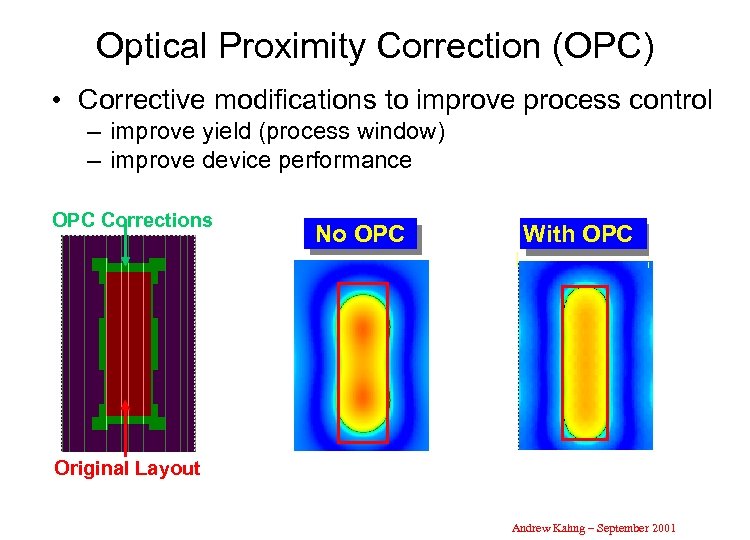
Optical Proximity Correction (OPC) • Corrective modifications to improve process control – improve yield (process window) – improve device performance OPC Corrections No OPC With OPC Original Layout Andrew Kahng – September 2001
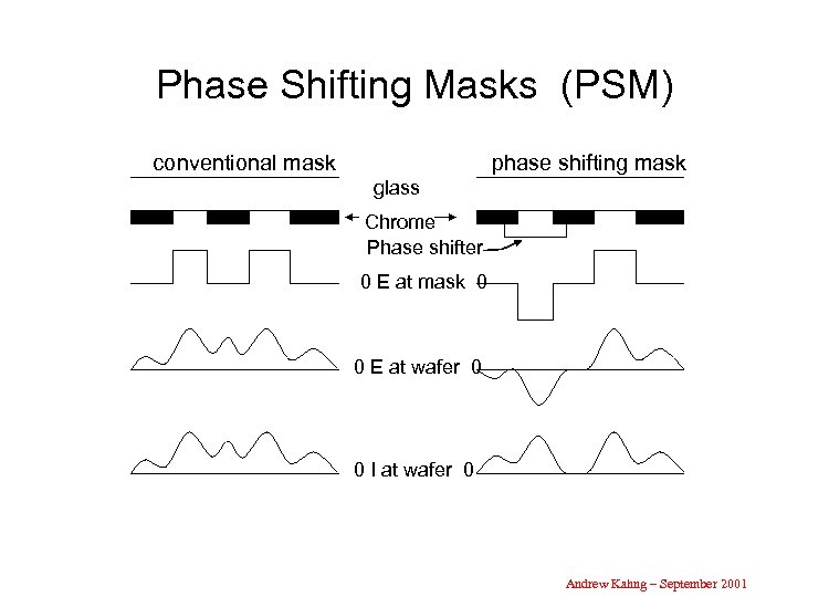
Phase Shifting Masks (PSM) conventional mask phase shifting mask glass Chrome Phase shifter 0 E at mask 0 0 E at wafer 0 0 I at wafer 0 Andrew Kahng – September 2001
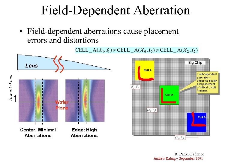
Field-Dependent Aberration • Field-dependent aberrations cause placement errors and distortions Towards Lens Wafer Plane Center: Minimal Aberrations Edge: High Aberrations R. Pack, Cadence Andrew Kahng – September 2001
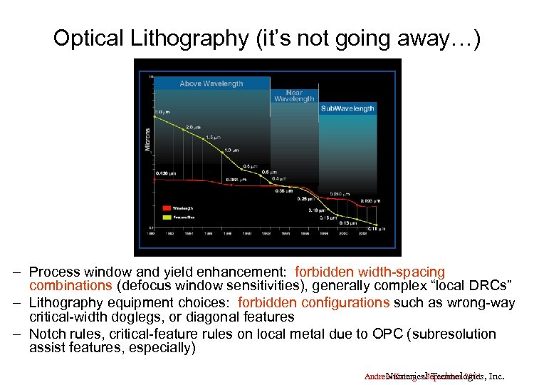
Optical Lithography (it’s not going away…) – Process window and yield enhancement: forbidden width-spacing combinations (defocus window sensitivities), generally complex “local DRCs” – Lithography equipment choices: forbidden configurations such as wrong-way critical-width doglegs, or diagonal features – Notch rules, critical-feature rules on local metal due to OPC (subresolution assist features, especially) Numerical Technologies, Inc. Andrew Kahng – September 2001
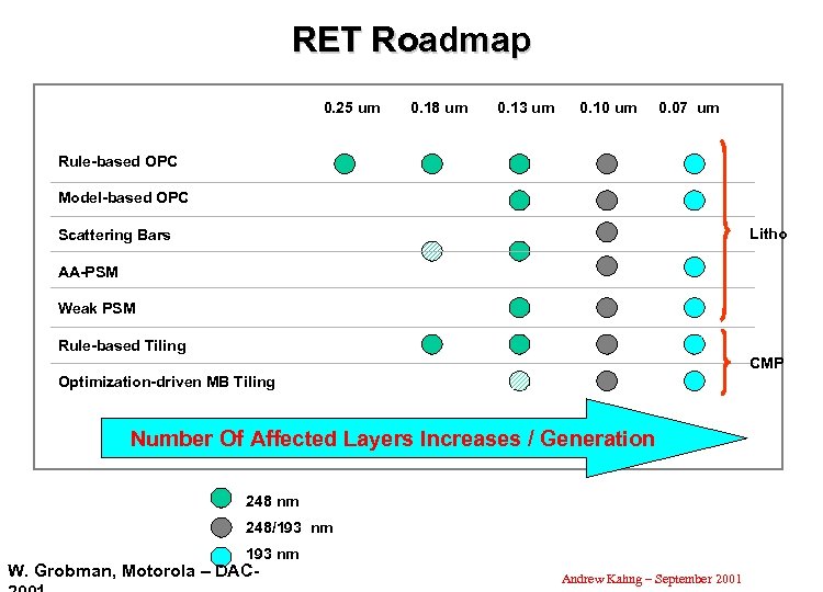
RET Roadmap 0. 25 um 0. 18 um 0. 13 um 0. 10 um 0. 07 um Rule-based OPC Model-based OPC Litho Scattering Bars AA-PSM Weak PSM Rule-based Tiling CMP Optimization-driven MB Tiling Number Of Affected Layers Increases / Generation 248 nm 248/193 nm W. Grobman, Motorola – DAC- Andrew Kahng – September 2001
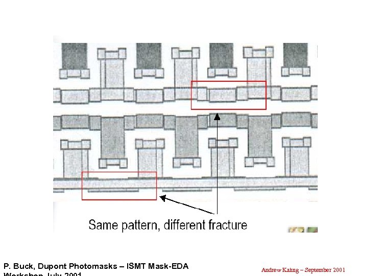
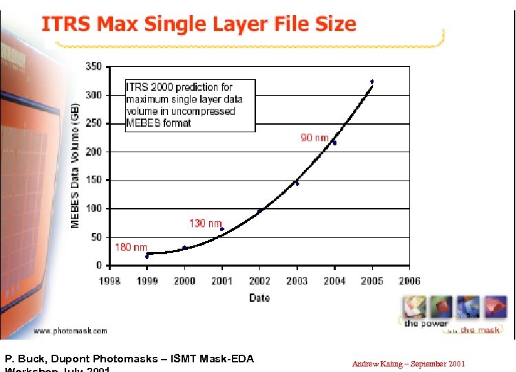
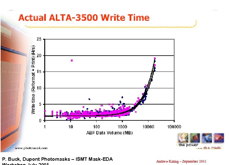
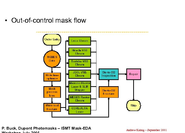
About Mask Data and $1 M Mask NRE • Format proliferation – Most tools have unique data format – Raster-VSB conversion, reverse can be inefficient – Real-time manufacturing tool switch, multiple qualified tools duplicate fractures to avoid delays if tool switch required • Data volume – – – OPC drives figure count acceleration MEBES format is flat ALTA machines slow down with > 1 GB data Burden on globally distributed mfg resources Inefficient refractures • Refractures!? – Mask industry historically never touched mask data: unwilling to take risk, not enough margin or reason – Today, 90% of mask data files manipulated / refractured: process bias sizing (iso-dense, loading effects, linearity, …), mask write optimization, multiple tool formats, … Andrew Kahng – September 2001
P. Buck, Dupont Photomasks – ISMT Mask-EDA Andrew Kahng – September 2001
P. Buck, Dupont Photomasks – ISMT Mask-EDA Andrew Kahng – September 2001
P. Buck, Dupont Photomasks – ISMT Mask-EDA Andrew Kahng – September 2001
• Out-of-control mask flow P. Buck, Dupont Photomasks – ISMT Mask-EDA Andrew Kahng – September 2001

DT Needs for RET and Mask NRE • WYSIWYG broken (mask) verification bottleneck • Need function- and cost-aware RET – RET insertion is for predictable circuit performance, function – RET tool must understand functional intent • make only corrections that win $$$, reduce performance variation • make only corrections that can be manufactured and verified (including mask inspection) • understand (data volume, verification) costs of breaking hierarchy – Understand flow issues • e. g. , avoid making same corrections 3 x (library, router, PV tool) • Handoff to manufacturing: MUCH more than GDSII – Includes sensitivities to patterning variation/error – Bidirectional pipe: functionally robust layout performed w. r. t. models of manufacturing errors and electrical implications – Mask verification driven by functional sensitivity information • Mask and ASIC folks aren’t asleep on this, either Andrew Kahng – September 2001

Another CANDE-01 Non-Prediction • Prediction: GDSII, in its present form, will no longer be the handoff from design to manufacturing. Andrew Kahng – September 2001

Riff #5: On Cost, Variability and Value Andrew Kahng – September 2001
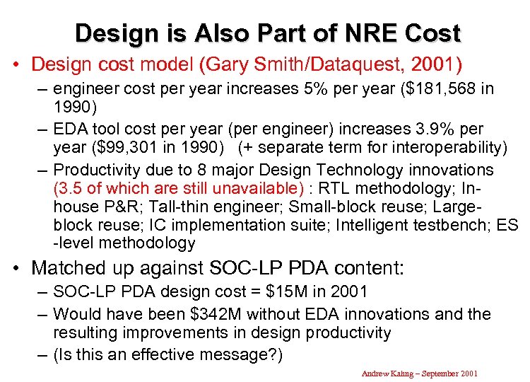
Design is Also Part of NRE Cost • Design cost model (Gary Smith/Dataquest, 2001) – engineer cost per year increases 5% per year ($181, 568 in 1990) – EDA tool cost per year (per engineer) increases 3. 9% per year ($99, 301 in 1990) (+ separate term for interoperability) – Productivity due to 8 major Design Technology innovations (3. 5 of which are still unavailable) : RTL methodology; Inhouse P&R; Tall-thin engineer; Small-block reuse; Largeblock reuse; IC implementation suite; Intelligent testbench; ES -level methodology • Matched up against SOC-LP PDA content: – SOC-LP PDA design cost = $15 M in 2001 – Would have been $342 M without EDA innovations and the resulting improvements in design productivity – (Is this an effective message? ) Andrew Kahng – September 2001
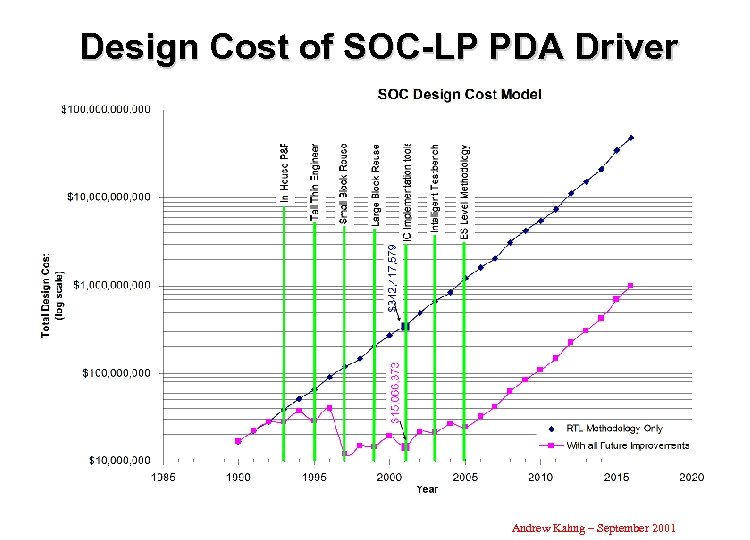
Design Cost of SOC-LP PDA Driver Andrew Kahng – September 2001
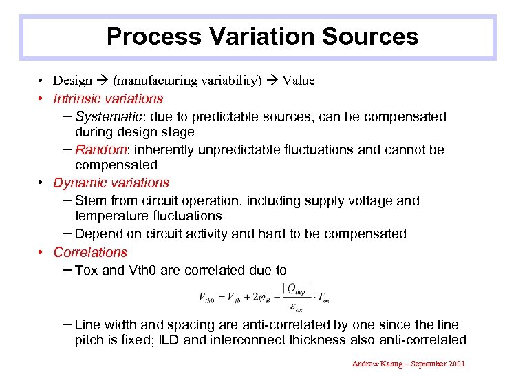
Process Variation Sources • Design (manufacturing variability) Value • Intrinsic variations – Systematic: due to predictable sources, can be compensated during design stage – Random: inherently unpredictable fluctuations and cannot be compensated • Dynamic variations – Stem from circuit operation, including supply voltage and temperature fluctuations – Depend on circuit activity and hard to be compensated • Correlations – Tox and Vth 0 are correlated due to – Line width and spacing are anti-correlated by one since the line pitch is fixed; ILD and interconnect thickness also anti-correlated Andrew Kahng – September 2001
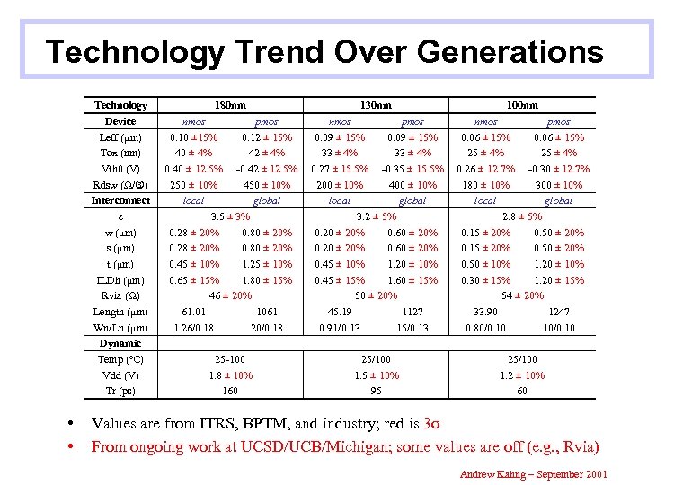
Technology Trend Over Generations Technology Device Leff (μm) Tox (nm) Vth 0 (V) Rdsw (Ω/ ) Interconnect ε w (μm) s (μm) t (μm) ILDh (μm) Rvia (Ω) Length (μm) Wn/Ln (μm) Dynamic Temp (o. C) Vdd (V) Tr (ps) • • 180 nm 130 nm 100 nm nmos pmos 0. 10 ± 15% 0. 12 ± 15% 40 ± 4% 42 ± 4% 0. 40 ± 12. 5% -0. 42 ± 12. 5% 250 ± 10% 450 ± 10% local global 3. 5 ± 3% 0. 28 ± 20% 0. 80 ± 20% 0. 45 ± 10% 1. 25 ± 10% 0. 65 ± 15% 1. 80 ± 15% 46 ± 20% 61. 01 1061 1. 26/0. 18 20/0. 18 nmos pmos 0. 09 ± 15% 33 ± 4% 0. 27 ± 15. 5% -0. 35 ± 15. 5% 200 ± 10% 400 ± 10% local global 3. 2 ± 5% 0. 20 ± 20% 0. 60 ± 20% 0. 45 ± 10% 1. 20 ± 10% 0. 45 ± 15% 1. 60 ± 15% 50 ± 20% 45. 19 1127 0. 91/0. 13 15/0. 13 nmos pmos 0. 06 ± 15% 25 ± 4% 0. 26 ± 12. 7% -0. 30 ± 12. 7% 180 ± 10% 300 ± 10% local global 2. 8 ± 5% 0. 15 ± 20% 0. 50 ± 10% 1. 20 ± 10% 0. 30 ± 15% 1. 20 ± 15% 54 ± 20% 33. 90 1247 0. 80/0. 10 10/0. 10 25 -100 1. 8 ± 10% 160 25/100 1. 5 ± 10% 95 25/100 1. 2 ± 10% 60 Values are from ITRS, BPTM, and industry; red is 3σ From ongoing work at UCSD/UCB/Michigan; some values are off (e. g. , Rvia) Andrew Kahng – September 2001
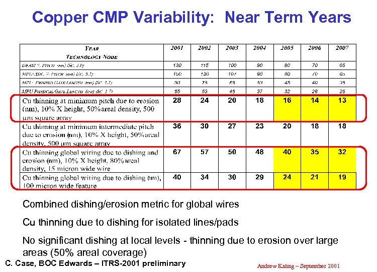
Copper CMP Variability: Near Term Years Combined dishing/erosion metric for global wires Cu thinning due to dishing for isolated lines/pads No significant dishing at local levels - thinning due to erosion over large areas (50% areal coverage) C. Case, BOC Edwards – ITRS-2001 preliminary Andrew Kahng – September 2001
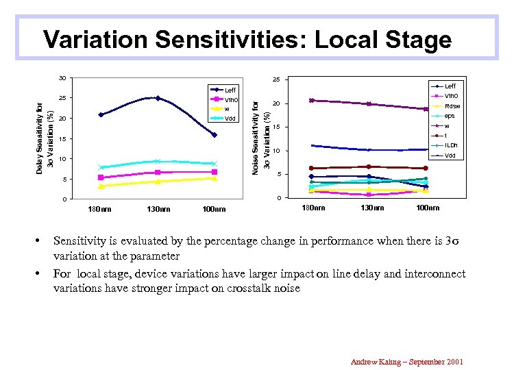
Variation Sensitivities: Local Stage 30 25 Leff w 20 Vdd 15 10 5 180 nm • Rdsw eps w 15 t ILDh 10 Vdd 5 0 0 • 20 3σ Variation (%) Vth 0 Noise Sensit 1 vity for Delay Sensitivity for 3σ Variation (%) 25 Vth 0 130 nm 100 nm 180 nm 130 nm 100 nm Sensitivity is evaluated by the percentage change in performance when there is 3σ variation at the parameter For local stage, device variations have larger impact on line delay and interconnect variations have stronger impact on crosstalk noise Andrew Kahng – September 2001
Value and Getting to ROI Andrew Kahng – September 2001

BTW: Need a Quality Model ? • “Normalized transistor” quality model normalizes: • • • speed, power, density in a given technology analog vs. digital custom vs. semi-custom vs. generated first-silicon success other: simple / complex clocking, verification/test effort and coverage, manufacturing cost, … • Need design and design process quality models? • strongly related to establishing DT value? • several private commercial and/or in-house analogues • survey methodology being contemplated by MARCO GSRC Andrew Kahng – September 2001

Riff #6: It’s Lunchtime Andrew Kahng – September 2001

Design Grand Challenges > 65 nm • Scaling of maximum-quality design implementation productivity • Overall design productivity of quality- (difficulty-) normalized functions on chip must scale at 2 x / node • Reuse (including migration) of design, verification and test effort must scale at > 2 x/node • Develop analog and mixed-signal synthesis, verification and test • Embedded software productivity • Power Management • Off-currents in low-power devices increase 10 x/node; design technology must maintain constant static power • Power dissipation for HP MPU exceeds package limits by 25 x in 15 years; design technology must achieve power limits • Power optimizations must simultaneously and fully exploit many degrees of freedom - multi-Vt, multi-Tox, multi-Vdd in core - while guiding architecture, OS and software • Deeper integration of Design technology with other ITRS technology areas • Example: Die-package co-optimization • Example: Design for Manufacturability (sharing variability burden with Litho/PIDS/FEP and Interconnect, reduction of system NRE cost) • Example: Design for Test ITRS-2001 preliminary Andrew Kahng – September 2001
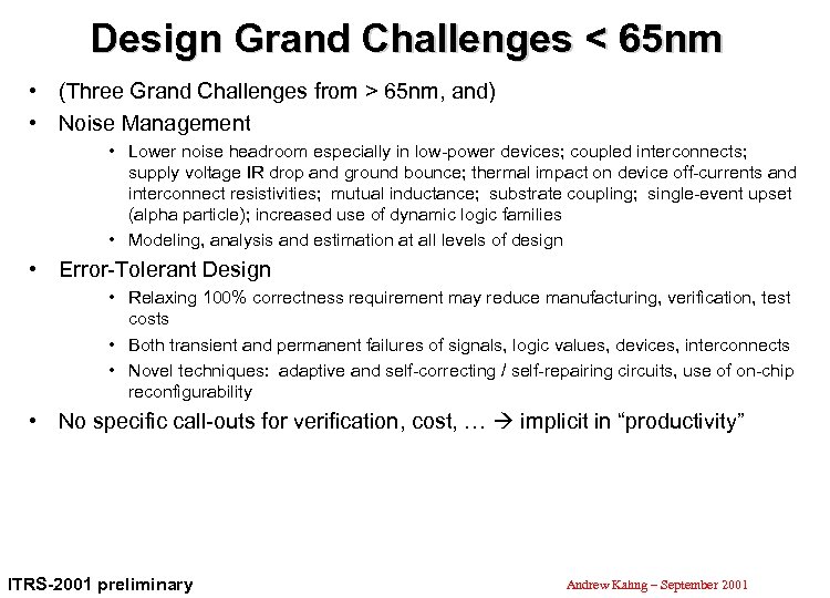
Design Grand Challenges < 65 nm • (Three Grand Challenges from > 65 nm, and) • Noise Management • Lower noise headroom especially in low-power devices; coupled interconnects; supply voltage IR drop and ground bounce; thermal impact on device off-currents and interconnect resistivities; mutual inductance; substrate coupling; single-event upset (alpha particle); increased use of dynamic logic families • Modeling, analysis and estimation at all levels of design • Error-Tolerant Design • Relaxing 100% correctness requirement may reduce manufacturing, verification, test costs • Both transient and permanent failures of signals, logic values, devices, interconnects • Novel techniques: adaptive and self-correcting / self-repairing circuits, use of on-chip reconfigurability • No specific call-outs for verification, cost, … implicit in “productivity” ITRS-2001 preliminary Andrew Kahng – September 2001

Conclusions • Design Technology needs to prove ROI – Prove quality and value – Prove costs: hidden costs include TAT/TTM; also include interoperability, integration, designer productivity… • Design Technology must show its Red Bricks – Need METRICS! (Design Chapter has almost no red/yellow/white) • Design Technology must share (take co-ownership of) other technology domains’ Red Bricks – Plenty of possibilities… • Design Technology community must educate itself and the rest of the ITRS community (esp. customers!) – Virtuous cycle: DT gives better ROI, achieves higher value, improves technology delivery, … Andrew Kahng – September 2001
ba5ce09981e1eb4564bbcbde3ff72a19.ppt