4c8810697e4837e39f7dc2f78ec25938.ppt
- Количество слайдов: 29
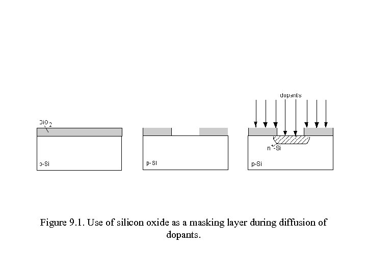 Figure 9. 1. Use of silicon oxide as a masking layer during diffusion of dopants.
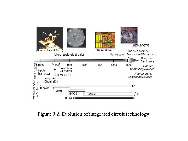 Figure 9. 2. Evolution of integrated circuit technology.
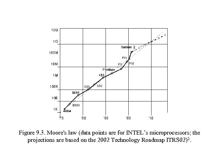 Figure 9. 3. Moore's law (data points are for INTEL’s microprocessors; the projections are based on the 2002 Technology Roadmap ITRS 02)2.
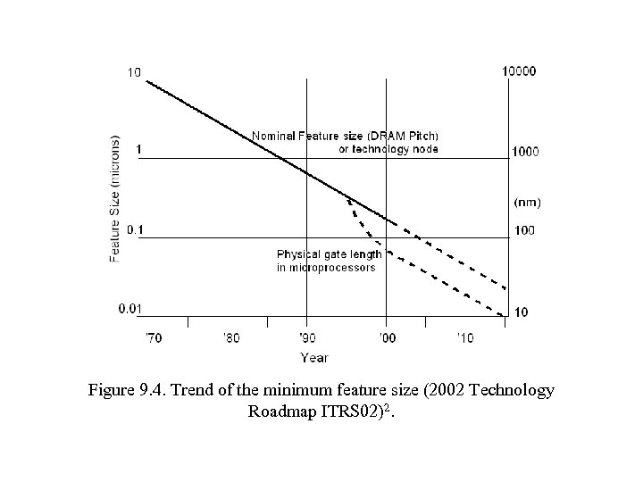 Figure 9. 4. Trend of the minimum feature size (2002 Technology Roadmap ITRS 02)2.
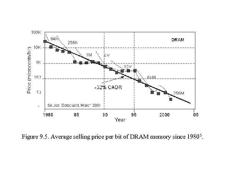 Figure 9. 5. Average selling price per bit of DRAM memory since 19805.
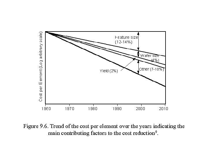 Figure 9. 6. Trend of the cost per element over the years indicating the main contributing factors to the cost reduction 9.
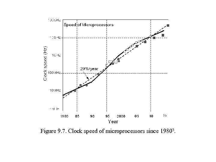 Figure 9. 7. Clock speed of microprocessors since 19805.
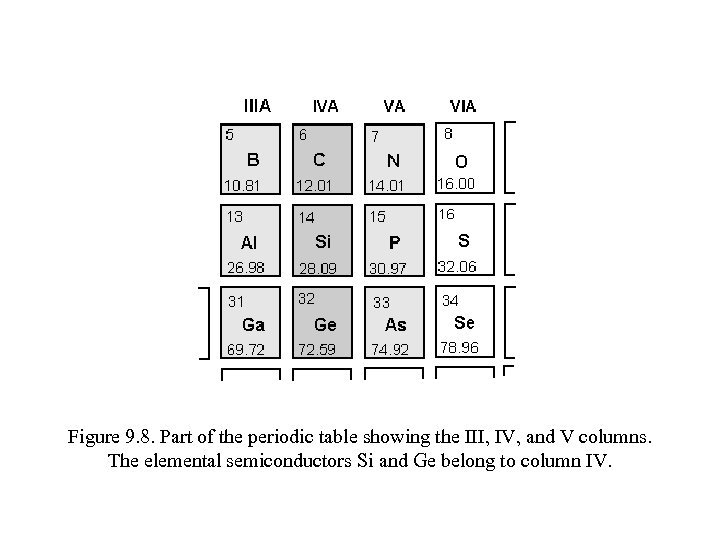 Figure 9. 8. Part of the periodic table showing the III, IV, and V columns. The elemental semiconductors Si and Ge belong to column IV.
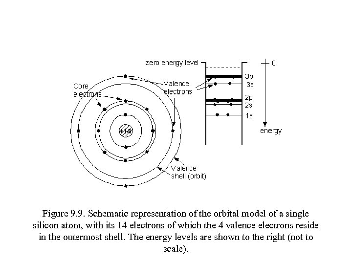 Figure 9. 9. Schematic representation of the orbital model of a single silicon atom, with its 14 electrons of which the 4 valence electrons reside in the outermost shell. The energy levels are shown to the right (not to scale).
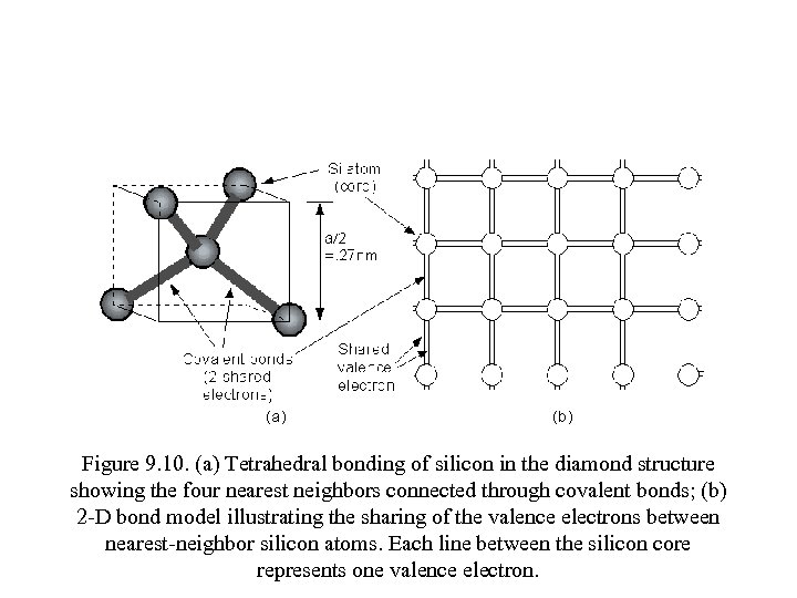 Figure 9. 10. (a) Tetrahedral bonding of silicon in the diamond structure showing the four nearest neighbors connected through covalent bonds; (b) 2 -D bond model illustrating the sharing of the valence electrons between nearest-neighbor silicon atoms. Each line between the silicon core represents one valence electron.
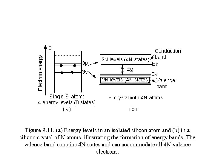 Figure 9. 11. (a) Energy levels in an isolated silicon atom and (b) in a silicon crystal of N atoms, illustrating the formation of energy bands. The valence band contains 4 N states and can accommodate all 4 N valence electrons.
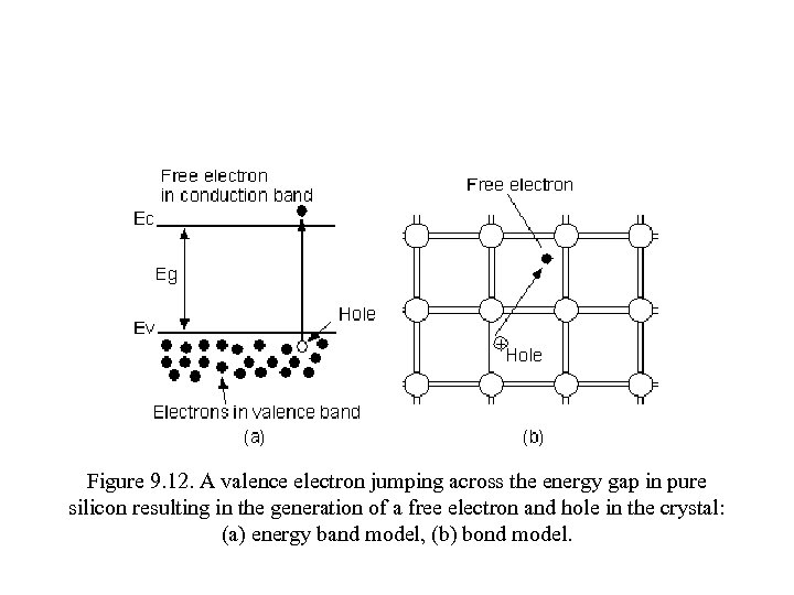 Figure 9. 12. A valence electron jumping across the energy gap in pure silicon resulting in the generation of a free electron and hole in the crystal: (a) energy band model, (b) bond model.
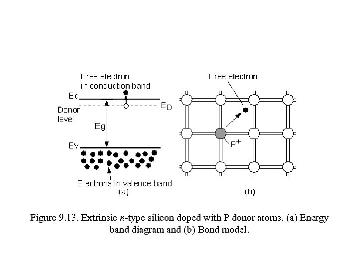 Figure 9. 13. Extrinsic n-type silicon doped with P donor atoms. (a) Energy band diagram and (b) Bond model.
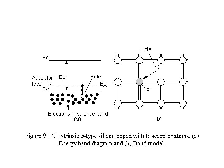 Figure 9. 14. Extrinsic p-type silicon doped with B acceptor atoms. (a) Energy band diagram and (b) Bond model.
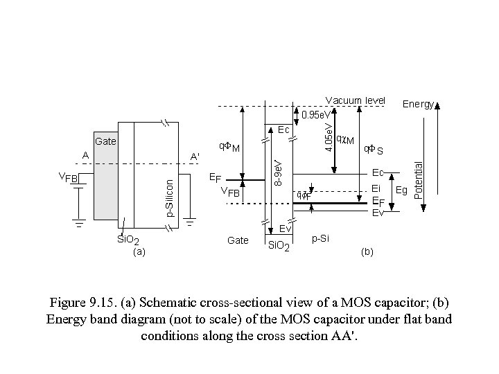 Figure 9. 15. (a) Schematic cross-sectional view of a MOS capacitor; (b) Energy band diagram (not to scale) of the MOS capacitor under flat band conditions along the cross section AA'.
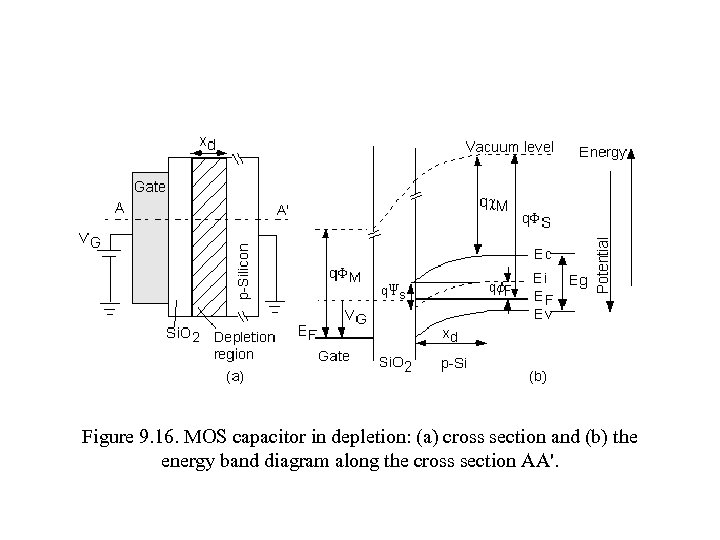 Figure 9. 16. MOS capacitor in depletion: (a) cross section and (b) the energy band diagram along the cross section AA'.
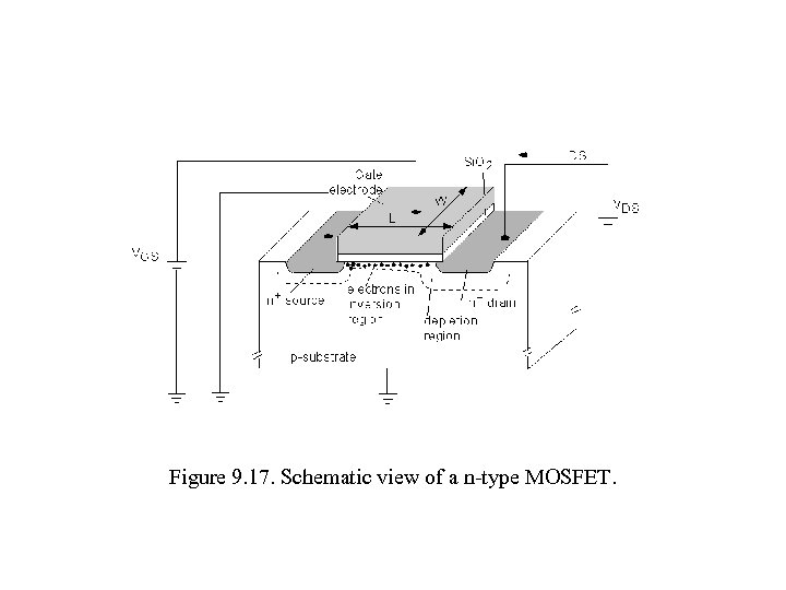 Figure 9. 17. Schematic view of a n-type MOSFET.
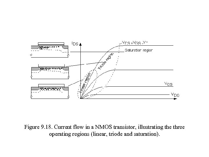 Figure 9. 18. Current flow in a NMOS transistor, illustrating the three operating regions (linear, triode and saturation).
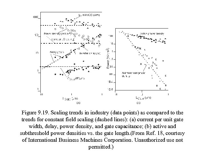 Figure 9. 19. Scaling trends in industry (data points) as compared to the trends for constant field scaling (dashed lines): (a) current per unit gate width, delay, power density, and gate capacitance; (b) active and subthreshold power densities vs. the gate length. (From Ref. 18, courtesy of International Business Machines Corporation. Unauthorized use not permitted. )
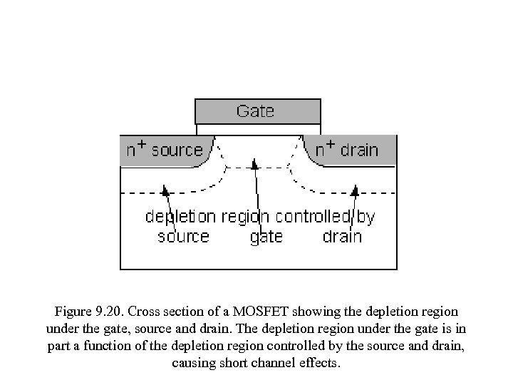 Figure 9. 20. Cross section of a MOSFET showing the depletion region under the gate, source and drain. The depletion region under the gate is in part a function of the depletion region controlled by the source and drain, causing short channel effects.
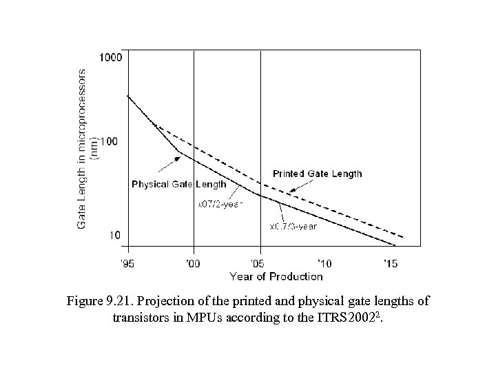 Figure 9. 21. Projection of the printed and physical gate lengths of transistors in MPUs according to the ITRS 20022.
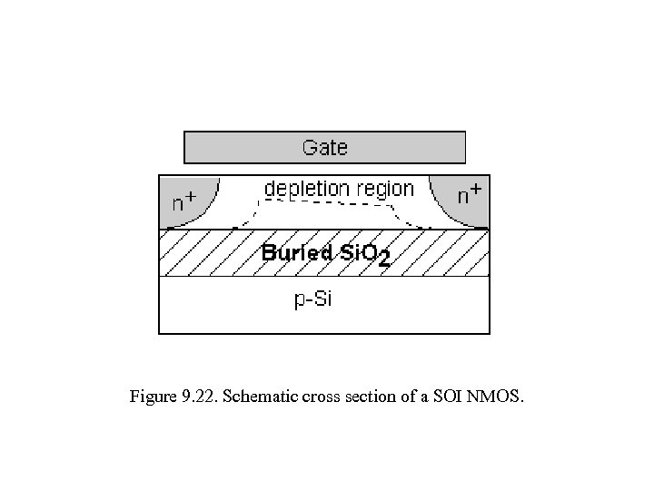 Figure 9. 22. Schematic cross section of a SOI NMOS.
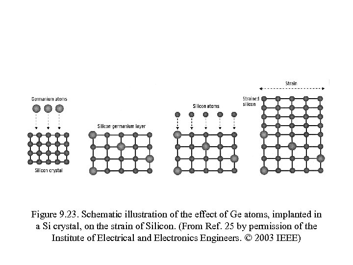 Figure 9. 23. Schematic illustration of the effect of Ge atoms, implanted in a Si crystal, on the strain of Silicon. (From Ref. 25 by permission of the Institute of Electrical and Electronics Engineers. © 2003 IEEE)
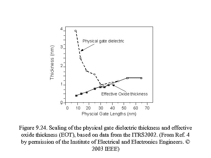 Figure 9. 24. Scaling of the physical gate dielectric thickness and effective oxide thickness (EOT), based on data from the ITRS 2002. (From Ref. 4 by permission of the Institute of Electrical and Electronics Engineers. © 2003 IEEE)
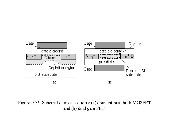 Figure 9. 25. Schematic cross sections: (a) conventional bulk MOSFET and (b) dual gate FET.
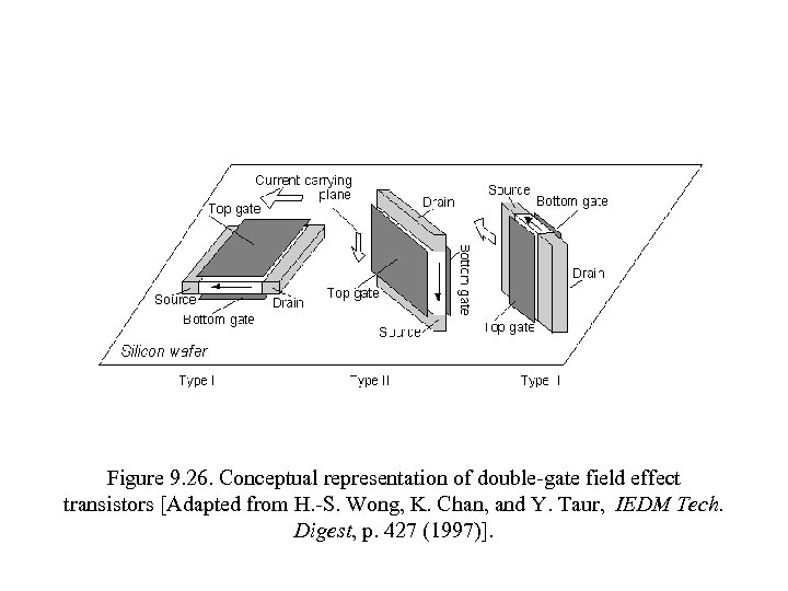 Figure 9. 26. Conceptual representation of double-gate field effect transistors [Adapted from H. -S. Wong, K. Chan, and Y. Taur, IEDM Tech. Digest, p. 427 (1997)].
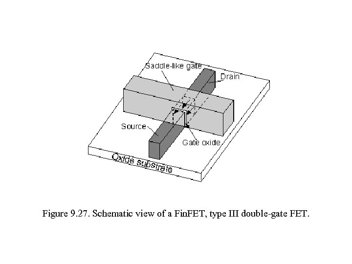 Figure 9. 27. Schematic view of a Fin. FET, type III double-gate FET.
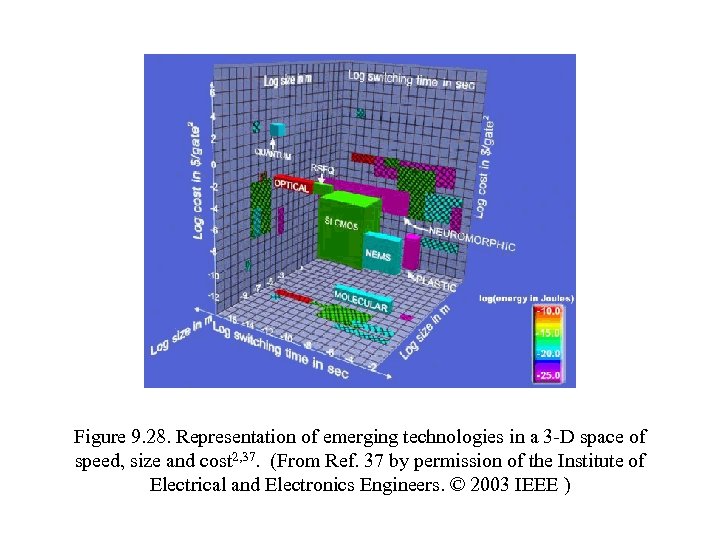 Figure 9. 28. Representation of emerging technologies in a 3 -D space of speed, size and cost 2, 37. (From Ref. 37 by permission of the Institute of Electrical and Electronics Engineers. © 2003 IEEE )
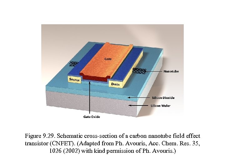 Figure 9. 29. Schematic cross-section of a carbon nanotube field effect transistor (CNFET). (Adapted from Ph. Avouris, Acc. Chem. Res. 35, 1026 (2002) with kind permission of Ph. Avouris. )


