38d199d07a01b49baa842fd386edeb38.ppt
- Количество слайдов: 21
 FEC: features and an application example J. Toledo Universidad Politécnica de Valencia NEXT Experiment
 Outline Ø A list of features in the FEC card Ø Prototype production schedule Ø FEC firmware development Ø Application: NEXT-1 phase of the NEXT experiment Pisa 24 -30 May 2009 Nadia Yahlali
 A list of features in the FEC card.
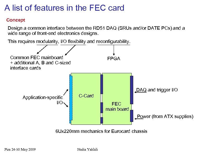 A list of features in the FEC card Concept Design a common interface between the RD 51 DAQ (SRUs and/or DATE PCs) and a wide range of front-end electronics designs. This requires modularity, I/O flexibility and reconfigurability. Common FEC mainboard + additional A, B and C-sized interface cards FPGA A-Card DAQ and trigger I/O Application-specific I/O C-Card B-Card FEC main board Power (from ATX supplies) 6 Ux 220 mm mechanics for Eurocard chassis Pisa 24 -30 May 2009 Nadia Yahlali
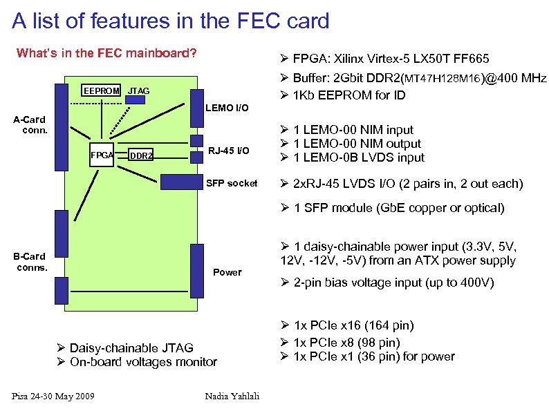 A list of features in the FEC card What’s in the FEC mainboard? EEPROM Ø FPGA: Xilinx Virtex-5 LX 50 T FF 665 Ø Buffer: 2 Gbit DDR 2(MT 47 H 128 M 16)@400 MHz Ø 1 Kb EEPROM for ID JTAG LEMO I/O A-Card conn. FPGA DDR 2 RJ-45 I/O SFP socket Ø 1 LEMO-00 NIM input Ø 1 LEMO-00 NIM output Ø 1 LEMO-0 B LVDS input Ø 2 x. RJ-45 LVDS I/O (2 pairs in, 2 out each) Ø 1 SFP module (Gb. E copper or optical) B-Card conns. Power Ø Daisy-chainable JTAG Ø On-board voltages monitor Pisa 24 -30 May 2009 Nadia Yahlali Ø 1 daisy-chainable power input (3. 3 V, 5 V, 12 V, -5 V) from an ATX power supply Ø 2 -pin bias voltage input (up to 400 V) Ø 1 x PCIe x 16 (164 pin) Ø 1 x PCIe x 8 (98 pin) Ø 1 x PCIe x 1 (36 pin) for power
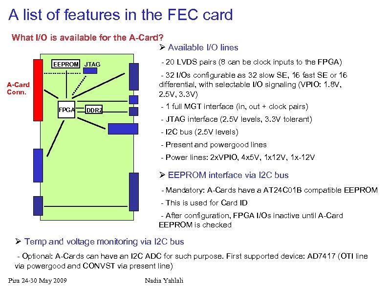 A list of features in the FEC card What I/O is available for the A-Card? Ø Available I/O lines EEPROM JTAG - 20 LVDS pairs (8 can be clock inputs to the FPGA) - 32 I/Os configurable as 32 slow SE, 16 fast SE or 16 differential, with selectable I/O signaling (VPIO: 1. 8 V, 2. 5 V, 3. 3 V) A-Card Conn. FPGA DDR 2 - 1 full MGT interface (in, out + clock pairs) - JTAG interface (2. 5 V levels, 3. 3 V tolerant) - I 2 C bus (2. 5 V levels) - Present and powergood lines - Power lines: 2 x. VPIO, 4 x 5 V, 1 x 12 V, 1 x-12 V Ø EEPROM interface via I 2 C bus - Mandatory: A-Cards have a AT 24 C 01 B compatible EEPROM - This is used for Card ID - After configuration, FPGA I/Os inactive until A-Card EEPROM is checked Ø Temp and voltage monitoring via I 2 C bus - Optional: A-Cards can have an I 2 C ADC for such purpose. First supported device: AD 7417 (OTI line via powergood and CONVST via present line) Pisa 24 -30 May 2009 Nadia Yahlali
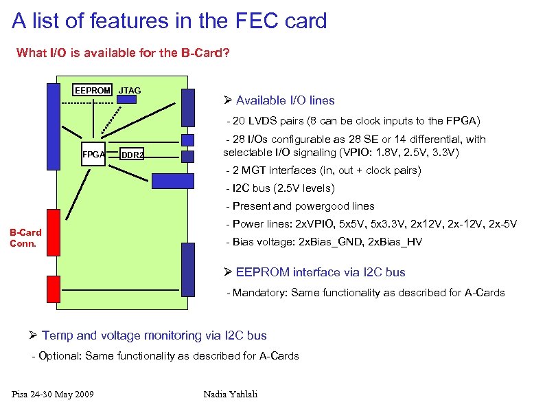 A list of features in the FEC card What I/O is available for the B-Card? EEPROM JTAG Ø Available I/O lines - 20 LVDS pairs (8 can be clock inputs to the FPGA) FPGA DDR 2 - 28 I/Os configurable as 28 SE or 14 differential, with selectable I/O signaling (VPIO: 1. 8 V, 2. 5 V, 3. 3 V) - 2 MGT interfaces (in, out + clock pairs) - I 2 C bus (2. 5 V levels) - Present and powergood lines B-Card Conn. - Power lines: 2 x. VPIO, 5 x 5 V, 5 x 3. 3 V, 2 x 12 V, 2 x-5 V - Bias voltage: 2 x. Bias_GND, 2 x. Bias_HV Ø EEPROM interface via I 2 C bus - Mandatory: Same functionality as described for A-Cards Ø Temp and voltage monitoring via I 2 C bus - Optional: Same functionality as described for A-Cards Pisa 24 -30 May 2009 Nadia Yahlali
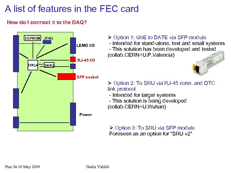 A list of features in the FEC card How do I connect it to the DAQ? EEPROM JTAG LEMO I/O Ø Option 1: Gb. E to DATE via SFP module - Intended for stand-alone, test and small systems - This solution has been developed and tested (collab. CERN+U. P. Valencia) RJ-45 I/O FPGA DDR 2 SFP socket Ø Option 2: To SRU via RJ-45 conn. and DTC link protocol - Intended for larger systems - This solution is being developed (collab. CERN+U. Wuhan) Power Ø Option 3: To SRU via SFP module Foreseen as an option for “SRU v 2” Pisa 24 -30 May 2009 Nadia Yahlali
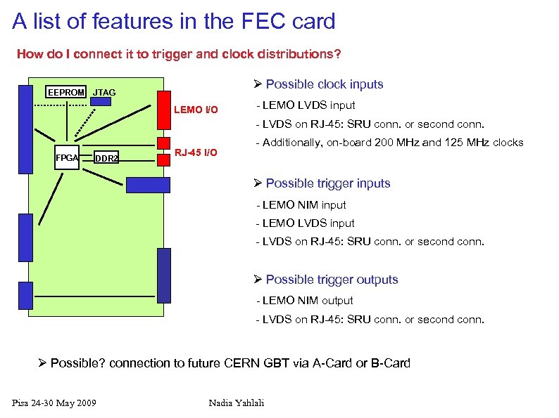 A list of features in the FEC card How do I connect it to trigger and clock distributions? EEPROM Ø Possible clock inputs JTAG LEMO I/O - LEMO LVDS input - LVDS on RJ-45: SRU conn. or second conn. FPGA DDR 2 RJ-45 I/O - Additionally, on-board 200 MHz and 125 MHz clocks Ø Possible trigger inputs - LEMO NIM input - LEMO LVDS input - LVDS on RJ-45: SRU conn. or second conn. Ø Possible trigger outputs - LEMO NIM output - LVDS on RJ-45: SRU conn. or second conn. Ø Possible? connection to future CERN GBT via A-Card or B-Card Pisa 24 -30 May 2009 Nadia Yahlali
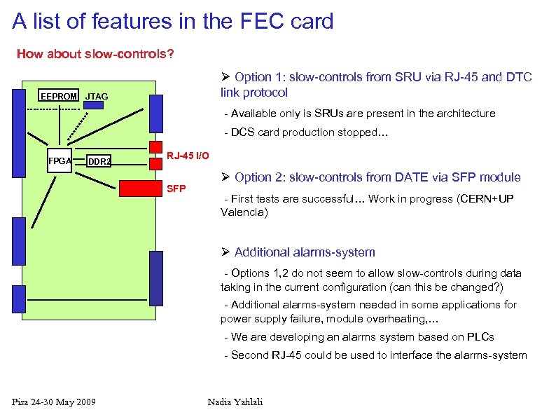 A list of features in the FEC card How about slow-controls? EEPROM Ø Option 1: slow-controls from SRU via RJ-45 and DTC link protocol JTAG - Available only is SRUs are present in the architecture - DCS card production stopped… FPGA DDR 2 RJ-45 I/O SFP Ø Option 2: slow-controls from DATE via SFP module - First tests are successful… Work in progress (CERN+UP Valencia) Ø Additional alarms-system - Options 1, 2 do not seem to allow slow-controls during data taking in the current configuration (can this be changed? ) - Additional alarms-system needed in some applications for power supply failure, module overheating, … - We are developing an alarms system based on PLCs - Second RJ-45 could be used to interface the alarms-system Pisa 24 -30 May 2009 Nadia Yahlali
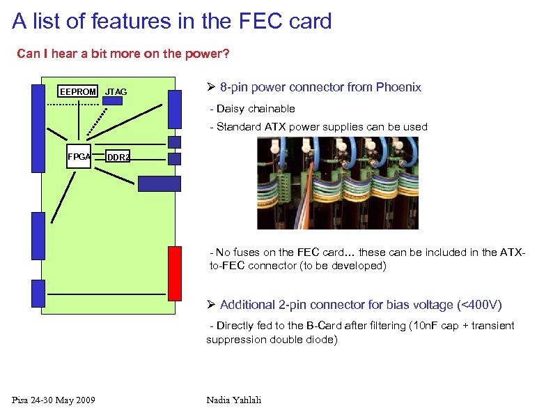 A list of features in the FEC card Can I hear a bit more on the power? EEPROM JTAG Ø 8 -pin power connector from Phoenix - Daisy chainable - Standard ATX power supplies can be used FPGA DDR 2 - No fuses on the FEC card… these can be included in the ATXto-FEC connector (to be developed) Ø Additional 2 -pin connector for bias voltage (<400 V) - Directly fed to the B-Card after filtering (10 n. F cap + transient suppression double diode) Pisa 24 -30 May 2009 Nadia Yahlali
 Prototype production schedule.
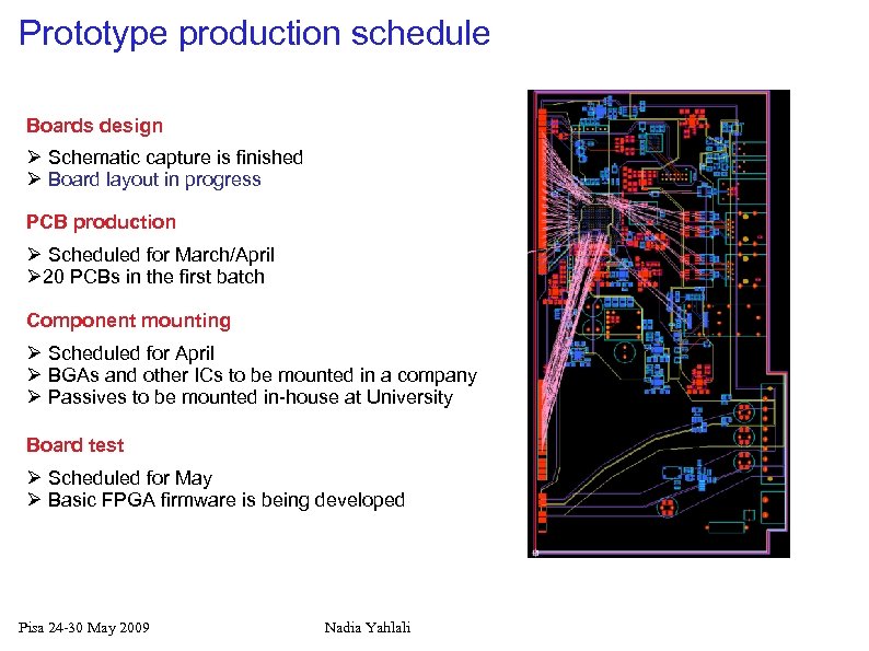 Prototype production schedule Boards design Ø Schematic capture is finished Ø Board layout in progress PCB production Ø Scheduled for March/April Ø 20 PCBs in the first batch Component mounting Ø Scheduled for April Ø BGAs and other ICs to be mounted in a company Ø Passives to be mounted in-house at University Board test Ø Scheduled for May Ø Basic FPGA firmware is being developed Pisa 24 -30 May 2009 Nadia Yahlali
 FEC firmware development. Ø We can provide a basic set of features to RD-51 users Ø Users must then add their application-specific code
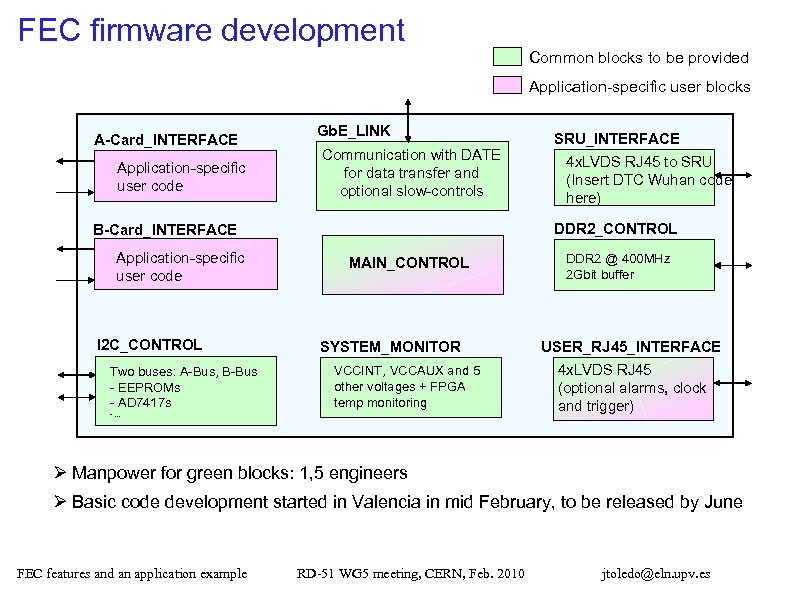 FEC firmware development Common blocks to be provided Application-specific user blocks A-Card_INTERFACE Application-specific user code Gb. E_LINK Communication with DATE for data transfer and optional slow-controls I 2 C_CONTROL Two buses: A-Bus, B-Bus - EEPROMs - AD 7417 s 4 x. LVDS RJ 45 to SRU (Insert DTC Wuhan code here) DDR 2_CONTROL B-Card_INTERFACE Application-specific user code SRU_INTERFACE MAIN_CONTROL SYSTEM_MONITOR VCCINT, VCCAUX and 5 other voltages + FPGA temp monitoring -… DDR 2 @ 400 MHz 2 Gbit buffer USER_RJ 45_INTERFACE 4 x. LVDS RJ 45 (optional alarms, clock and trigger) Ø Manpower for green blocks: 1, 5 engineers Ø Basic code development started in Valencia in mid February, to be released by June FEC features and an application example RD-51 WG 5 meeting, CERN, Feb. 2010 jtoledo@eln. upv. es
 First application: NEXT-1 phase of the NEXT experiment.
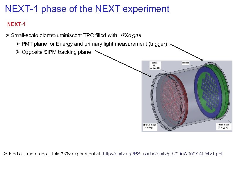 NEXT-1 phase of the NEXT experiment NEXT-1 Ø Small-scale electroluminiscent TPC filled with 136 Xe gas Ø PMT plane for Energy and primary light measurement (trigger) Ø Opposite Si. PM tracking plane Ø Find out more about this bb 0 n experiment at: http: //arxiv. org/PS_cache/arxiv/pdf/0907. 4054 v 1. pdf
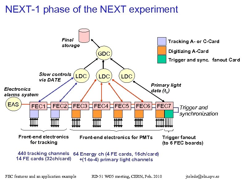 NEXT-1 phase of the NEXT experiment Final storage Tracking A- or C-Card Digitizing A-Card GDC Trigger and sync. fanout Card Slow controls LDC via DATE LDC Primary light data (to) Electronics alarms system EAS FEC 1 FEC 2 FEC 3 Front-end electronics for tracking FEC 4 FEC 5 FEC 6 FEC 7 Front-end electronics for PMTs Trigger and synchronization Trigger fanout (to 6 FEC boards) 440 tracking channels 64 Energy ch (4 FE cards, 16 ch/card) 14 FE cards (32 ch/card) +(1 -to-4) primary light channels FEC features and an application example RD-51 WG 5 meeting, CERN, Feb. 2010 jtoledo@eln. upv. es
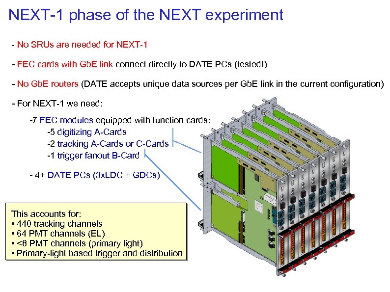 NEXT-1 phase of the NEXT experiment - No SRUs are needed for NEXT-1 - FEC cards with Gb. E link connect directly to DATE PCs (tested!) - No Gb. E routers (DATE accepts unique data sources per Gb. E link in the current configuration) - For NEXT-1 we need: -7 FEC modules equipped with function cards: -5 digitizing A-Cards -2 tracking A-Cards or C-Cards -1 trigger fanout B-Card - 4+ DATE PCs (3 x. LDC + GDCs) This accounts for: • 440 tracking channels • 64 PMT channels (EL) • <8 PMT channels (primary light) • Primary-light based trigger and distribution
 NEXT-1 phase of the NEXT experiment Interface to the front-end electronics Ø Analog front-end (PMTs): we receive 16 analog differential signals and send an I 2 C control bus for channel settings - 68 -pin VHDCI connector with differential pinout? - 50 -pin D Sub? - Flat cable? ØDigital front-end (Si. PMs) for tracking: 4 x. LVDS RJ-45 connector, full duplex: clock+data in each direction (similar to FEC-SRU LVDS link) - FEC-to-frontend data: short frames with timestamp sync, trigger and monitoring request - Frontend-to-FEC data: digitized sensor data + monitoring response - We will not power the front-end from the FEC - We will digitally control the Si. PM bias from the FEC
 Thank you !


