f527c59c97b8e600154c9c2651787da6.ppt
- Количество слайдов: 54

f WEBENCH® Power Designer Power Supply Design Made Easy Dr Ali Shirsavar Biricha Digital Power Ltd Parkway Drive Reading RG 4 6 XG Dec - 2013 © Biricha Digital Power Ltd (unless stated otherwise) – material subject to NDA
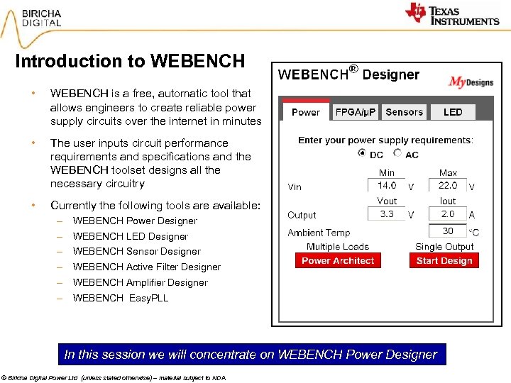
Introduction to WEBENCH • WEBENCH is a free, automatic tool that allows engineers to create reliable power supply circuits over the internet in minutes • The user inputs circuit performance requirements and specifications and the WEBENCH toolset designs all the necessary circuitry • Currently the following tools are available: – WEBENCH Power Designer – WEBENCH LED Designer – WEBENCH Sensor Designer – WEBENCH Active Filter Designer – WEBENCH Amplifier Designer – WEBENCH Easy. PLL In this session we will concentrate on WEBENCH Power Designer © Biricha Digital Power Ltd (unless stated otherwise) – material subject to NDA
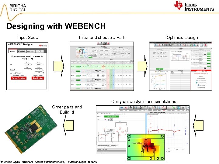
Designing with WEBENCH Input Spec Filter and choose a Part Optimize Design Carry out analysis and simulations Order parts and Build It! © Biricha Digital Power Ltd (unless stated otherwise) – material subject to NDA
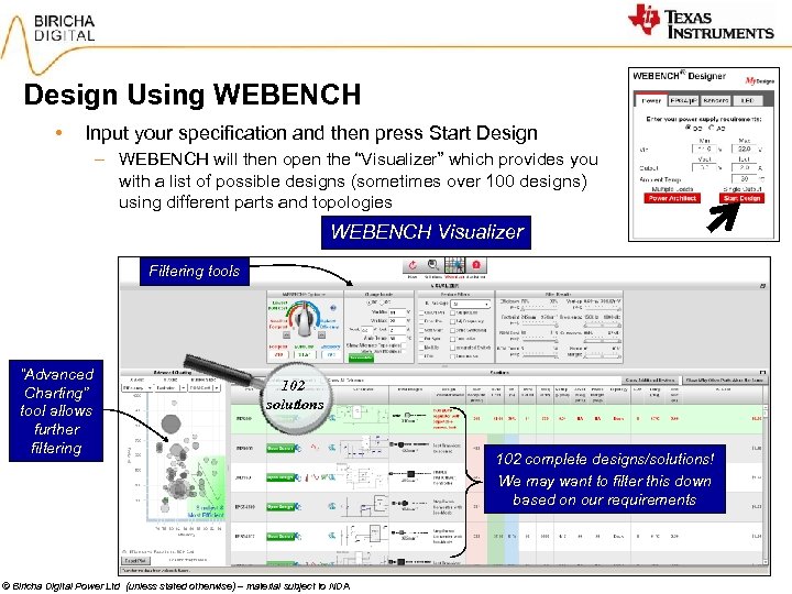
Design Using WEBENCH • Input your specification and then press Start Design – WEBENCH will then open the “Visualizer” which provides you with a list of possible designs (sometimes over 100 designs) using different parts and topologies WEBENCH Visualizer Filtering tools “Advanced Charting” tool allows further filtering 102 solutions © Biricha Digital Power Ltd (unless stated otherwise) – material subject to NDA 102 complete designs/solutions! We may want to filter this down based on our requirements
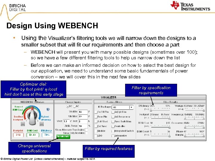
Design Using WEBENCH • Using the Visualizer’s filtering tools we will narrow down the designs to a smaller subset that will fit our requirements and then choose a part – WEBENCH will present you with many possible designs (sometimes over 100); so we have a few different filtering tools to help us narrow down the list – Before we can make an informed decision on how to select the best design for our application, we need to understand some basic fundamentals of power conversion – we will cover this in the next few slides Optimizer dial: Filter by foot print/ /cost hint don’t use at this early stage Change universal specifications Filter by specification requirements Filter by required features © Biricha Digital Power Ltd (unless stated otherwise) – material subject to NDA
WEBENCH Power Designer* • You can use WEBENCH to create customized power supplies or DC -DC converters for your circuits – This environment gives you end-to-end power supply designs and prototyping tools • WEBENCH tools enable you to solve switching-power-supply design problems before you build your prototype – This alleviates the time and trouble associated with traditional power supply design methods • Included in the WEBENCH toolset is a device selection tool – This tool helps you find the best switching regulator or MOSFET controller for your power supply circuit. It even selects the most appropriate passive components * Taken from http: //www. ti. com/lsds/ti/analog/webench/power. page © Biricha Digital Power Ltd (unless stated otherwise) – material subject to NDA
Topologies Used in WEBENCH • WEBENCH supports the following topologies – Buck – Boost – Inverting Buck-Boost – SEPIC – Flyback • These topologies cover almost all your point of load (POL) needs – There are other topologies not supported by WEBENCH but these are for very high power off-line power supplies and rarely used for POL power distribution within a PCB • WEBENCH automatically recommends the most suitable topology for you – But we will compare these topologies so that you have a better insight as to which topology is most suitable for your application © Biricha Digital Power Ltd (unless stated otherwise) – material subject to NDA
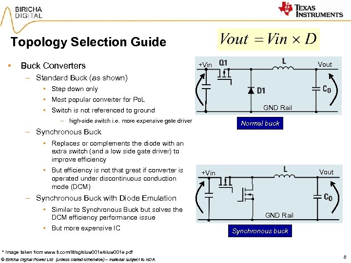
Topology Selection Guide • Buck Converters Vout +Vin – Standard Buck (as shown) • Step down only • Most popular converter for Po. L GND Rail • Switch is not referenced to ground – high-side switch i. e. more expensive gate driver Normal buck – Synchronous Buck • Replaces or complements the diode with an extra switch (and a low side gate driver) to improve efficiency • But efficiency is not that great if converter is operated under discontinuous conduction mode (DCM) Vout +Vin – Synchronous Buck with Diode Emulation • Similar to Synchronous Buck but solves the DCM efficiency performance issue • But more expensive IC * Image taken from www. ti. com/lit/sg/sluw 001 e. pdf © Biricha Digital Power Ltd (unless stated otherwise) – material subject to NDA GND Rail Synchronous buck 8
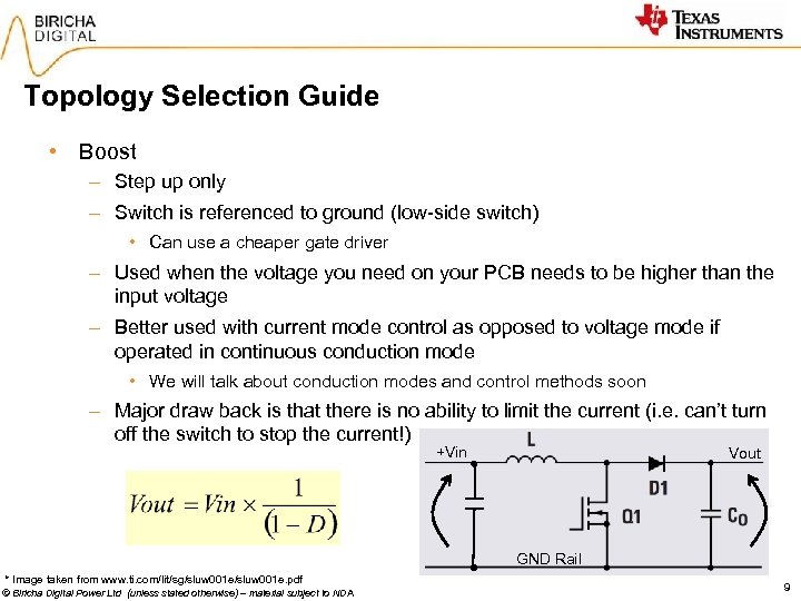
Topology Selection Guide • Boost – Step up only – Switch is referenced to ground (low-side switch) • Can use a cheaper gate driver – Used when the voltage you need on your PCB needs to be higher than the input voltage – Better used with current mode control as opposed to voltage mode if operated in continuous conduction mode • We will talk about conduction modes and control methods soon – Major draw back is that there is no ability to limit the current (i. e. can’t turn off the switch to stop the current!) +Vin Vout GND Rail * Image taken from www. ti. com/lit/sg/sluw 001 e. pdf © Biricha Digital Power Ltd (unless stated otherwise) – material subject to NDA 9
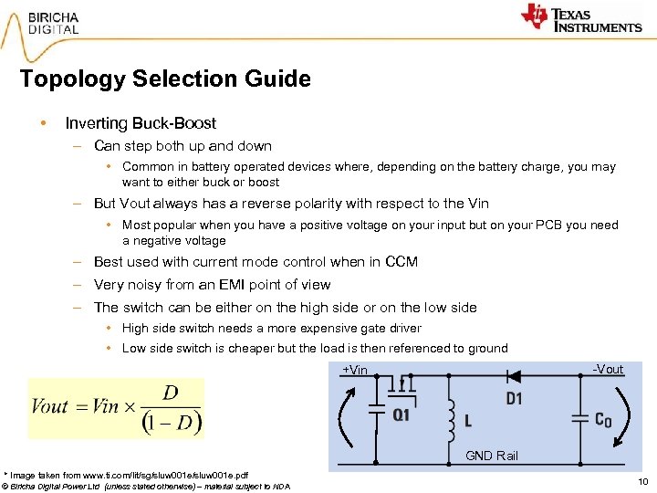
Topology Selection Guide • Inverting Buck-Boost – Can step both up and down • Common in battery operated devices where, depending on the battery charge, you may want to either buck or boost – But Vout always has a reverse polarity with respect to the Vin • Most popular when you have a positive voltage on your input but on your PCB you need a negative voltage – Best used with current mode control when in CCM – Very noisy from an EMI point of view – The switch can be either on the high side or on the low side • High side switch needs a more expensive gate driver • Low side switch is cheaper but the load is then referenced to ground -Vout +Vin GND Rail * Image taken from www. ti. com/lit/sg/sluw 001 e. pdf © Biricha Digital Power Ltd (unless stated otherwise) – material subject to NDA 10
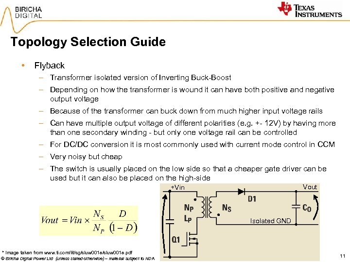
Topology Selection Guide • Flyback – Transformer isolated version of Inverting Buck-Boost – Depending on how the transformer is wound it can have both positive and negative output voltage – Because of the transformer can buck down from much higher input voltage rails – Can have multiple output voltage of different polarities (e. g. +- 12 V) by having more than one secondary winding - but only one voltage rail can be controlled – For DC/DC conversion it is most commonly used with current mode control in CCM – Very noisy but cheap – The switch is usually placed on the low side so that a cheaper gate driver can be used but it can also be placed on the high-side Vout +Vin Isolated GND * Image taken from www. ti. com/lit/sg/sluw 001 e. pdf © Biricha Digital Power Ltd (unless stated otherwise) – material subject to NDA 11
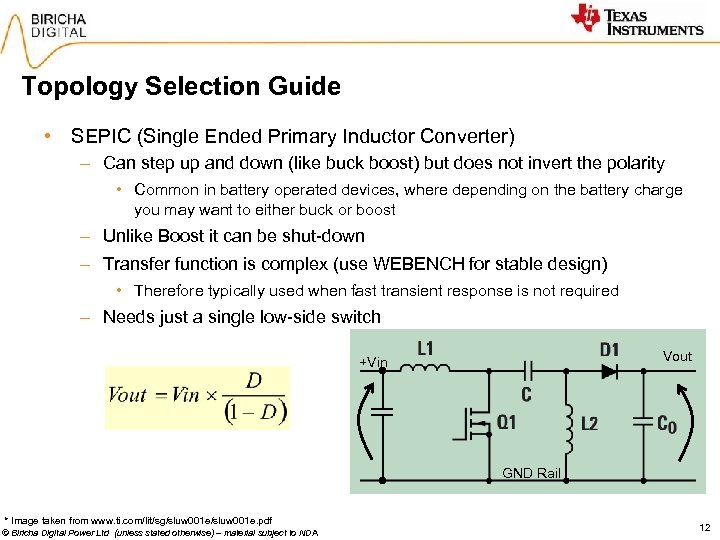
Topology Selection Guide • SEPIC (Single Ended Primary Inductor Converter) – Can step up and down (like buck boost) but does not invert the polarity • Common in battery operated devices, where depending on the battery charge you may want to either buck or boost – Unlike Boost it can be shut-down – Transfer function is complex (use WEBENCH for stable design) • Therefore typically used when fast transient response is not required – Needs just a single low-side switch Vout +Vin GND Rail * Image taken from www. ti. com/lit/sg/sluw 001 e. pdf © Biricha Digital Power Ltd (unless stated otherwise) – material subject to NDA 12
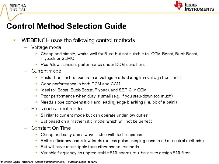
Control Method Selection Guide • WEBENCH uses the following control methods – Voltage mode • Cheap and simple; works well for Buck but not suitable for CCM Boost, Buck-Boost, Flyback or SEPIC • Poor/slow transient performance under DCM conditions – Current mode • • • Faster transient response than voltage mode during line voltage transients Good performance in both DCM and CCM Ideal for Boost, Buck-Boost, Flyback and SEPIC in CCM Poor performance when duty is small (e. g. if you step-down too much) Needs slope compensation and leading edge blanking (i. e. bit of a pain!) – Emulated current mode • Similar to current mode but can operate under low duties • But based on a mathematic model which will not be perfect – Constant On Time • • Cheap and easy and always stable with fast response Better efficiency under low loads (unless pulse skipping used in other control methods) But will have more ripple than other control methods Variable frequency so unpredictable EMI spectrum + harder to design EMI filter © Biricha Digital Power Ltd (unless stated otherwise) – material subject to NDA
Choosing the Right Switching Frequency • Our switching frequency (Fs) directly impacts the size of our power supply – We saw earlier that the higher the switching frequency the smaller the current ripple on our inductor • i. e. the higher the switching frequency, the smaller the inductor • This also applies to our output capacitor, so the entire power supply will get smaller • This is why the switching frequency of the PSU for small hand held devices needs to be so high • There is a limit as to the ripple we can have on our inductor as you must not saturate the inductor WEBENCH automatically selects a correctly sized inductor • Our switching frequency directly impacts our efficiency – The higher the switching frequency the poorer the efficiency • Every time we turn a switch on or off we will waste some energy; these are called Switching Losses if we switch faster we will have higher switching losses • Every time we magnetize and de-magnetize our inductor we will lose some energy in the magnetic material of our inductor; these are called Core Losses if we switch faster we will have higher core losses • Of course both of the above will have an impact on cost WEBENCH can optimize your design for efficiency or size or cost depending on your requirements © Biricha Digital Power Ltd (unless stated otherwise) – material subject to NDA
Choosing the Right Part/Device for Your Application • There are 4 major categories of ICs that WEBENCH designs with: – LDOs • Not recommended for good efficiency, output current above 500 m. A or large voltage drops – Switching Power Modules – Switching Regulators – Switching Controllers • Within seconds WEBENCH calculates over 100 designs with this parts • Which one is the most suitable for your application? – We will now quickly go through these categories – Once you know what the differences are you can very quickly use WEBENCH’s filtering tools to narrow down these 100 designs to just a handful most suitable for your application © Biricha Digital Power Ltd (unless stated otherwise) – material subject to NDA
Quick Summary to Selection Guide • Which topologies to use for various applications: – LDOs Small currents and limited/fixed voltages, poor efficiency – Buck most common step down – Boost most common step up – Buck-Boost/SEPIC most common for battery operation / step up and down – Flyback when you need multiple voltage or need to step down from large input voltage • Which control mode to use for various applications? – COT cheap and easy, always stable but variable frequency & ripple – Voltage mode most common in Buck, cheap and easy low component count – Current mode most common for CCM in Boost, Buck-Boost, SEPIC, Flyback, very good performance but needs slope compensation and leading edge blanking (a bit of a pain), not great if duty is very small – Emulated Current Mode like current mode but solved the low duty issue, but model based so it all depends on how accurate the model is © Biricha Digital Power Ltd (unless stated otherwise) – material subject to NDA
Quick Summary to Selection Guide • Selecting the switching frequency – The higher our Fs, the smaller the PSU but the poorer the efficiency – The higher the Fs the smaller the ripple on the inductor large ripple on inductor could cause saturation and a blown up power supply – WEBENCH allows you to automatically optimize this • Which Device to Select? – Switching Modules (almost) everything internal, smallest foot print, quickest and easiest to set up but more expensive – Switching Regulators Internal switch but external inductor, larger foot print than a module, more flexible due to external components, cheaper (if you don’t count the price of the inductor) – Switching Controllers just a PWM controller, so almost everything else is external, largest foot print, largest Bo. M, development time and routing but most flexible We are now ready to move on to Step 3 of designing with WEBENCH © Biricha Digital Power Ltd (unless stated otherwise) – material subject to NDA
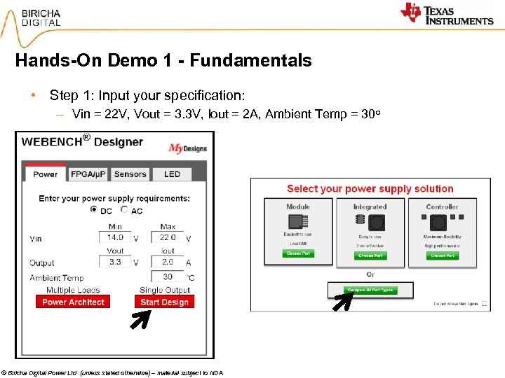
Hands-On Demo 1 - Fundamentals • Step 1: Input your specification: – Vin = 22 V, Vout = 3. 3 V, Iout = 2 A, Ambient Temp = 30 o © Biricha Digital Power Ltd (unless stated otherwise) – material subject to NDA
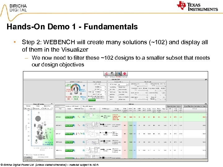
Hands-On Demo 1 - Fundamentals • Step 2: WEBENCH will create many solutions (~102) and display all of them in the Visualizer – We now need to filter these ~102 designs to a smaller subset that meets our design objectives © Biricha Digital Power Ltd (unless stated otherwise) – material subject to NDA
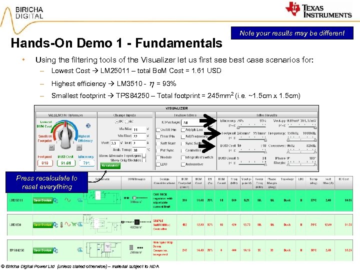
Hands-On Demo 1 - Fundamentals • Note your results may be different Using the filtering tools of the Visualizer let us first see best case scenarios for: – Lowest Cost LM 25011 – total Bo. M Cost = 1. 61 USD – Highest efficiency LM 3510 - = 93% – Smallest footprint TPS 84250 – Total footprint = 245 mm 2 (i. e. ~1. 5 cm x 1. 5 cm) Press recalculate to reset everything © Biricha Digital Power Ltd (unless stated otherwise) – material subject to NDA
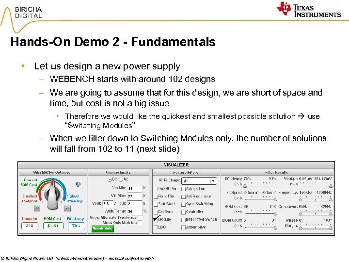
Hands-On Demo 2 - Fundamentals • Let us design a new power supply – WEBENCH starts with around 102 designs – We are going to assume that for this design, we are short of space and time, but cost is not a big issue • Therefore we would like the quickest and smallest possible solution use “Switching Modules” – When we filter down to Switching Modules only, the number of solutions will fall from 102 to 11 (next slide) © Biricha Digital Power Ltd (unless stated otherwise) – material subject to NDA
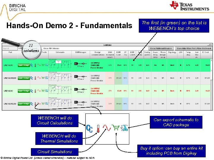
Hands-On Demo 2 - Fundamentals The first (in green) on the list is WEBENCH’s top choice 11 solutions WEBENCH will do Circuit Calculations Can export schematic to CAD package WEBENCH will do Thermal Simulations Circuit Simulations © Biricha Digital Power Ltd (unless stated otherwise) – material subject to NDA Buy it option: can buy an entire kit including PCB from Digikey
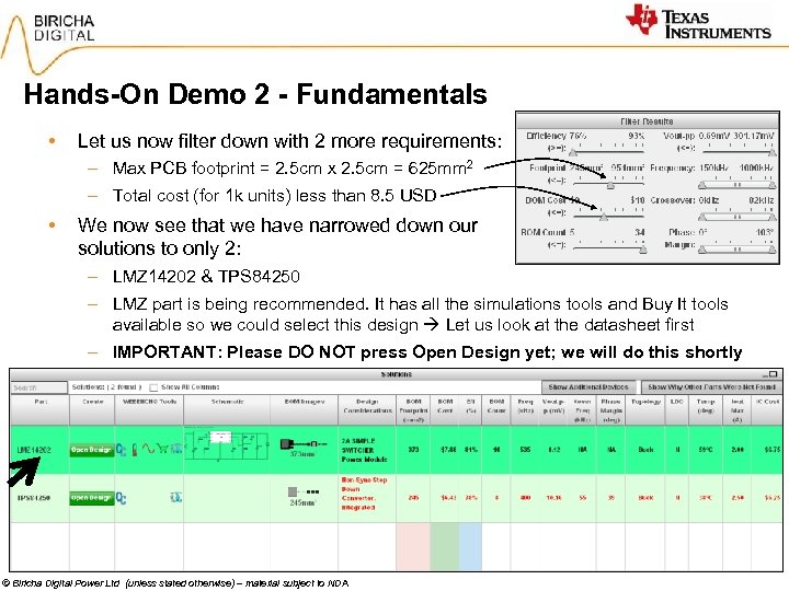
Hands-On Demo 2 - Fundamentals • Let us now filter down with 2 more requirements: – Max PCB footprint = 2. 5 cm x 2. 5 cm = 625 mm 2 – Total cost (for 1 k units) less than 8. 5 USD • We now see that we have narrowed down our solutions to only 2: – LMZ 14202 & TPS 84250 – LMZ part is being recommended. It has all the simulations tools and Buy It tools available so we could select this design Let us look at the datasheet first – IMPORTANT: Please DO NOT press Open Design yet; we will do this shortly © Biricha Digital Power Ltd (unless stated otherwise) – material subject to NDA
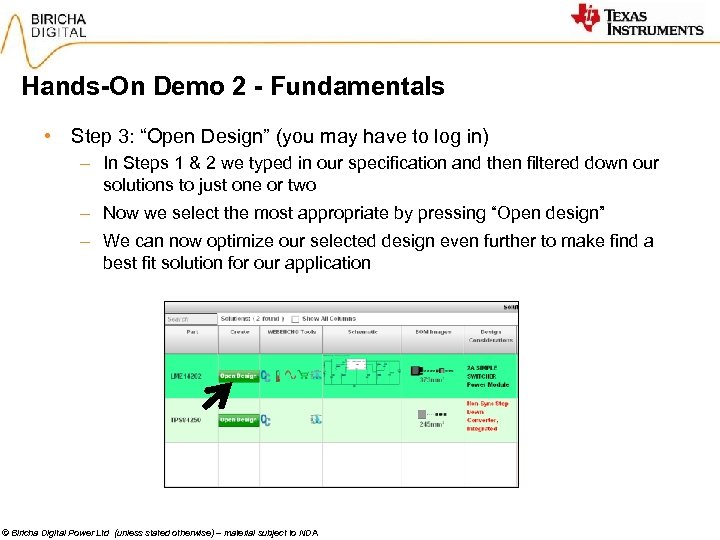
Hands-On Demo 2 - Fundamentals • Step 3: “Open Design” (you may have to log in) – In Steps 1 & 2 we typed in our specification and then filtered down our solutions to just one or two – Now we select the most appropriate by pressing “Open design” – We can now optimize our selected design even further to make find a best fit solution for our application © Biricha Digital Power Ltd (unless stated otherwise) – material subject to NDA
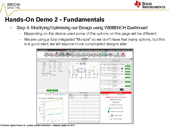
Hands-On Demo 2 - Fundamentals • Step 4: Modifying/Optimising our Design using WEBENCH Dashboard – Depending on the device used some of the options on this page will be different – We are using a fully integrated “Module” so we don’t have that many options, but this is a good start; we will explore more complicated designs later © Biricha Digital Power Ltd (unless stated otherwise) – material subject to NDA
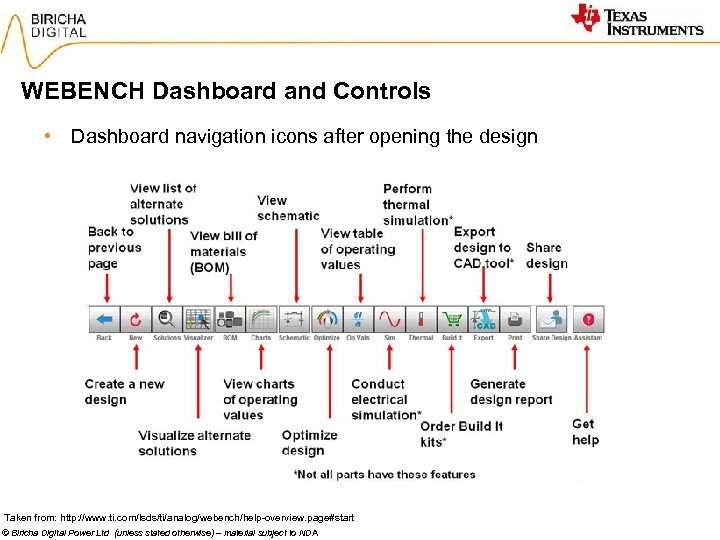
WEBENCH Dashboard and Controls • Dashboard navigation icons after opening the design Taken from: http: //www. ti. com/lsds/ti/analog/webench/help-overview. page#start © Biricha Digital Power Ltd (unless stated otherwise) – material subject to NDA
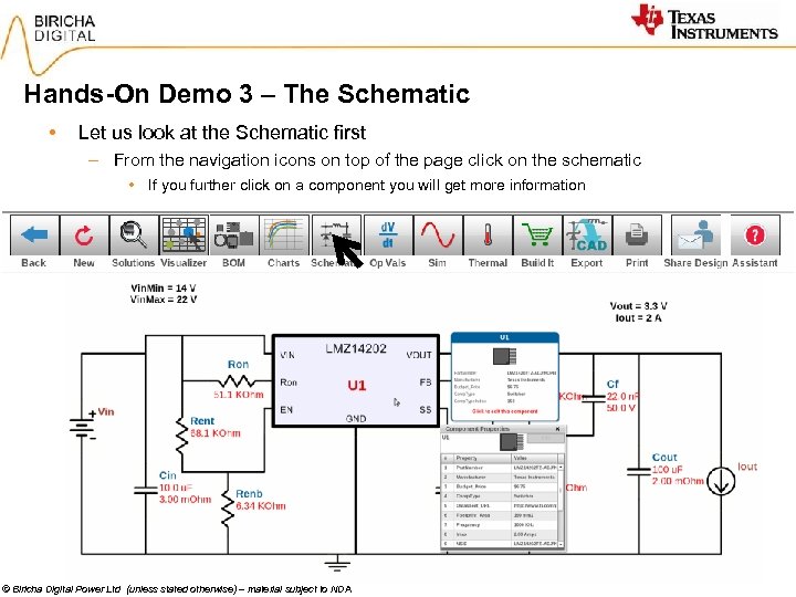
Hands-On Demo 3 – The Schematic • Let us look at the Schematic first – From the navigation icons on top of the page click on the schematic • If you further click on a component you will get more information © Biricha Digital Power Ltd (unless stated otherwise) – material subject to NDA
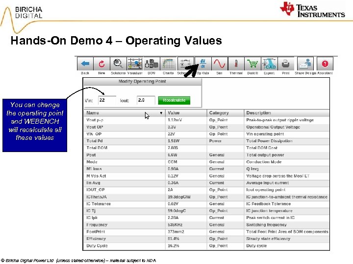
Hands-On Demo 4 – Operating Values You can change the operating point and WEBENCH will recalculate all these values © Biricha Digital Power Ltd (unless stated otherwise) – material subject to NDA
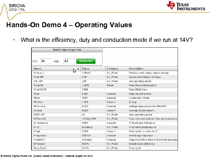
Hands-On Demo 4 – Operating Values • What is the efficiency, duty and conduction mode if we run at 14 V? © Biricha Digital Power Ltd (unless stated otherwise) – material subject to NDA
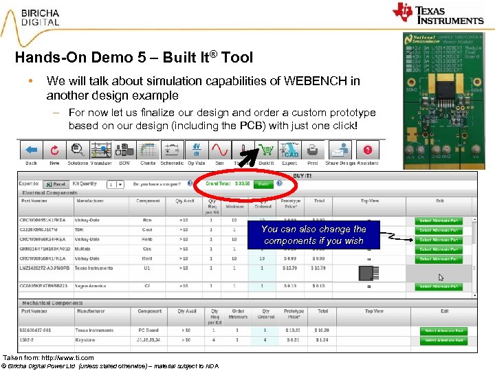
Hands-On Demo 5 – Built It® Tool • We will talk about simulation capabilities of WEBENCH in another design example – For now let us finalize our design and order a custom prototype based on our design (including the PCB) with just one click! You can also change the components if you wish Taken from: http: //www. ti. com © Biricha Digital Power Ltd (unless stated otherwise) – material subject to NDA
WEBENCH Optimization Tips and Tricks • In the previous slides we designed a Buck converter starting from a specification to a prototype within minutes • In the process we became familiar with some of the most important WEBENCH tools – Designer, Visualizer, filtering tools and Dashboard – Within Dashboard we used • Schematic tool • Operating Values • Built it tool • We will now design a more complicated power supply and become familiar with the Optimization tools available within WEBENCH © Biricha Digital Power Ltd (unless stated otherwise) – material subject to NDA
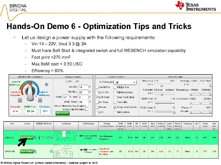
Hands-On Demo 6 - Optimization Tips and Tricks • Let us design a power supply with the following requirements: – Vin 14 – 22 V; Vout 3. 3 @ 2 A – Must have Soft Start & integrated switch and full WEBENCH simulation capability – Foot print <270 mm 2 – Max Bo. M cost < 3. 50 USD – Efficiency > 83% © Biricha Digital Power Ltd (unless stated otherwise) – material subject to NDA
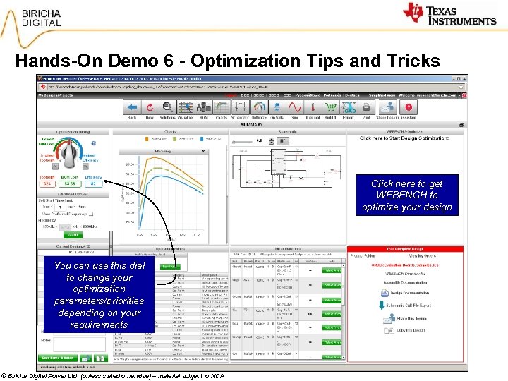
Hands-On Demo 6 - Optimization Tips and Tricks Click here to get WEBENCH to optimize your design You can use this dial to change your optimization parameters/priorities depending on your requirements © Biricha Digital Power Ltd (unless stated otherwise) – material subject to NDA
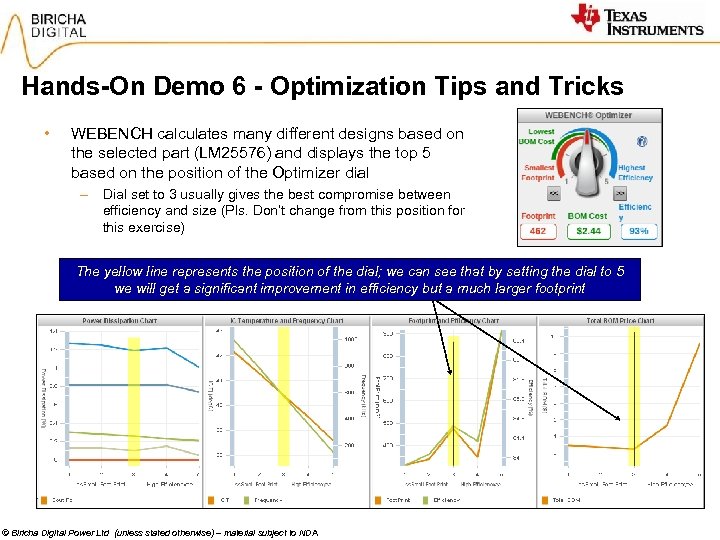
Hands-On Demo 6 - Optimization Tips and Tricks • WEBENCH calculates many different designs based on the selected part (LM 25576) and displays the top 5 based on the position of the Optimizer dial – Dial set to 3 usually gives the best compromise between efficiency and size (Pls. Don’t change from this position for this exercise) The yellow line represents the position of the dial; we can see that by setting the dial to 5 we will get a significant improvement in efficiency but a much larger footprint © Biricha Digital Power Ltd (unless stated otherwise) – material subject to NDA
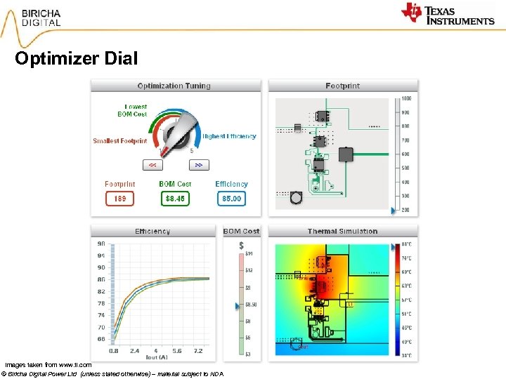
Optimizer Dial Images taken from www. ti. com © Biricha Digital Power Ltd (unless stated otherwise) – material subject to NDA
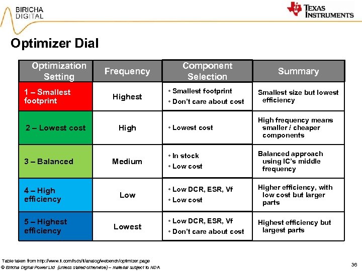
Optimizer Dial Optimization Setting 1 – Smallest footprint 2 – Lowest cost 3 – Balanced 4 – High efficiency 5 – Highest efficiency Frequency Component Selection Summary Highest • Smallest footprint • Don’t care about cost Smallest size but lowest efficiency • Lowest cost High frequency means smaller / cheaper components • In stock • Low cost Balanced approach using IC’s middle frequency • Low DCR, ESR, Vf • Low cost Higher efficiency, with low cost but larger parts • Low DCR, ESR, Vf • Don’t care about cost Highest efficiency but largest parts High Medium Lowest Table taken from http: //www. ti. com/lsds/ti/analog/webench/optimizer. page © Biricha Digital Power Ltd (unless stated otherwise) – material subject to NDA 36
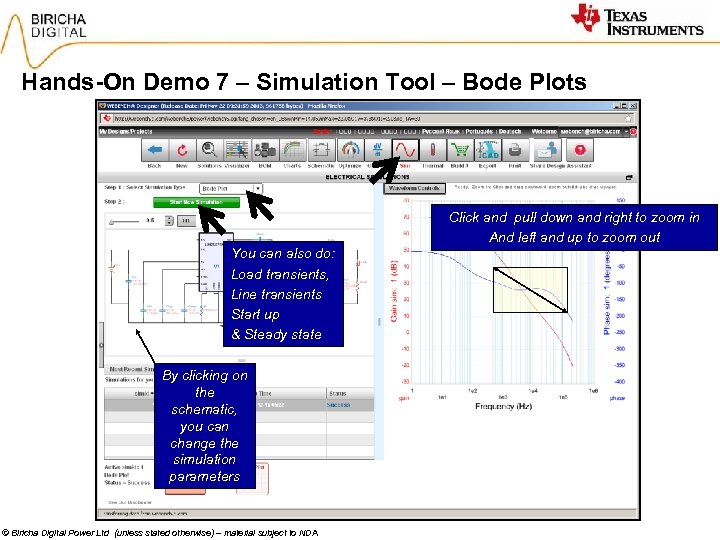
Hands-On Demo 7 – Simulation Tool – Bode Plots Click and pull down and right to zoom in And left and up to zoom out You can also do: Load transients, Line transients Start up & Steady state By clicking on the schematic, you can change the simulation parameters © Biricha Digital Power Ltd (unless stated otherwise) – material subject to NDA
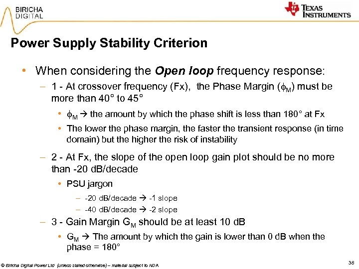
Power Supply Stability Criterion • When considering the Open loop frequency response: – 1 - At crossover frequency (Fx), the Phase Margin ( M) must be more than 40° to 45° • M the amount by which the phase shift is less than 180° at Fx • The lower the phase margin, the faster the transient response (in time domain) but the higher the risk of instability – 2 - At Fx, the slope of the open loop gain plot should be no more than -20 d. B/decade • PSU jargon – -20 d. B/decade -1 slope – -40 d. B/decade -2 slope – 3 - Gain Margin GM should be at least 10 d. B • GM The amount by which the gain is lower than 0 d. B when the phase = 180° © Biricha Digital Power Ltd (unless stated otherwise) – material subject to NDA 38
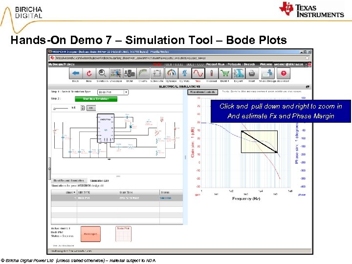
Hands-On Demo 7 – Simulation Tool – Bode Plots Click and pull down and right to zoom in And estimate Fx and Phase Margin © Biricha Digital Power Ltd (unless stated otherwise) – material subject to NDA
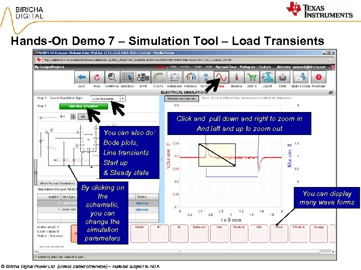
Hands-On Demo 7 – Simulation Tool – Load Transients You can also do: Bode plots, Line transients Start up & Steady state By clicking on the schematic, you can change the simulation parameters © Biricha Digital Power Ltd (unless stated otherwise) – material subject to NDA Click and pull down and right to zoom in And left and up to zoom out You can display many wave forms
Thermal Simulation with Web. THERMTM • Web. THERM™ online tool simulates thermal behavior of an electronic printed circuit board – Using validated thermal models for the components and the reference PCB – The user defines the environment, air flow, copper thickness, presence of fan/heat sink, etc – Takes into account thermal interaction of different components adjacent to each other – The Web. THERM tools helps the user identify heat problems on the printed circuit board • i. e. the board goes into production. – A simulation typically takes two to three minutes to complete, – After the simulation is complete, the user can view the result, a full colour plot of the temperature across the board – The temperature of each component is also listed in an accompanying table – If desired, the user can adjust the parameters and resubmit the job for simulation Taken from: www. ti. com/lsds/ti/analog/webench/thermal-simulation. page © Biricha Digital Power Ltd (unless stated otherwise) – material subject to NDA 41
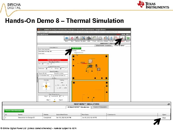
Hands-On Demo 8 – Thermal Simulation © Biricha Digital Power Ltd (unless stated otherwise) – material subject to NDA
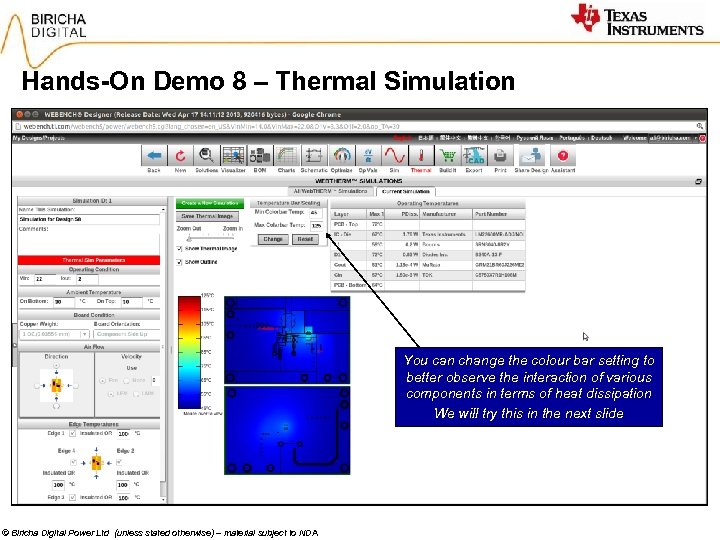
Hands-On Demo 8 – Thermal Simulation You can change the colour bar setting to better observe the interaction of various components in terms of heat dissipation We will try this in the next slide © Biricha Digital Power Ltd (unless stated otherwise) – material subject to NDA
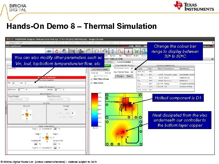
Hands-On Demo 8 – Thermal Simulation You can also modify other parameters such as Vin, Iout, top/bottom temperature/air flow, etc Change the colour bar range to display between 30 o to 60 o. C Hottest component is D 1 Heat dissipated from the vias underneath our controller to the bottom layer copper © Biricha Digital Power Ltd (unless stated otherwise) – material subject to NDA
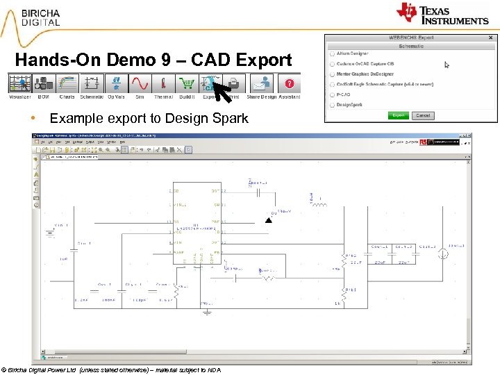
Hands-On Demo 9 – CAD Export • Example export to Design Spark © Biricha Digital Power Ltd (unless stated otherwise) – material subject to NDA
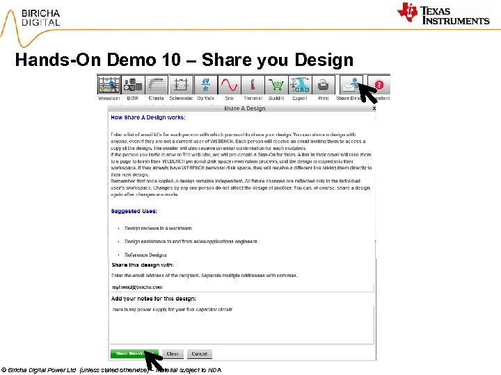
Hands-On Demo 10 – Share you Design © Biricha Digital Power Ltd (unless stated otherwise) – material subject to NDA
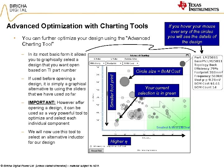
Advanced Optimization with Charting Tools • You can further optimize your design using the “Advanced Charting Tool” – In its most basic form it allows you to graphically select a design that you want open based on TI part number – IMPORTANT: However after opening a design, it can be used as a very powerful tool to optimize and select each individual component – We will now use this tool to select an alternative inductor for our design © Biricha Digital Power Ltd (unless stated otherwise) – material subject to NDA Circle size = Bo. M Cost Smaller foot print – If used before opening a design, it is simply a graphical alternative to using the sliders that we have used so far If you hover your mouse over any of the circles you will see the details of the design Higher Your current selection is in green
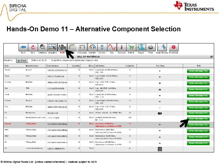
Hands-On Demo 11 – Alternative Component Selection © Biricha Digital Power Ltd (unless stated otherwise) – material subject to NDA
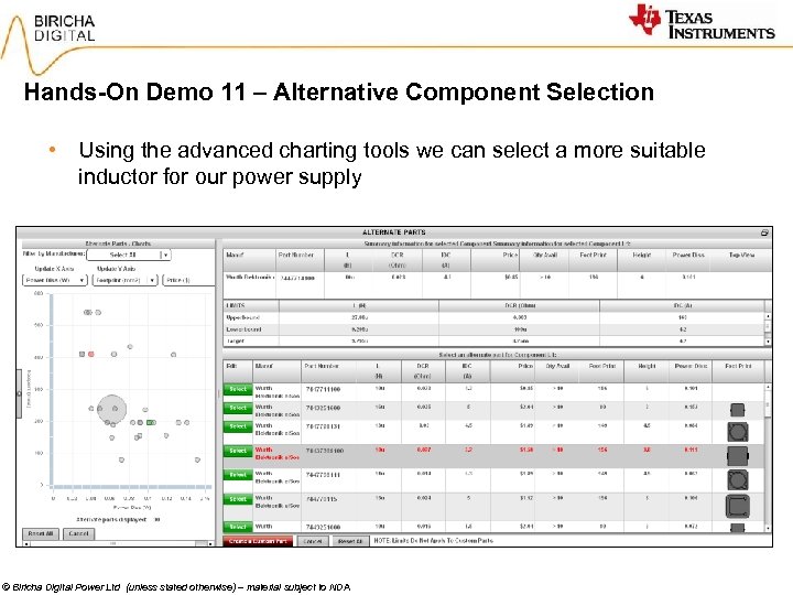
Hands-On Demo 11 – Alternative Component Selection • Using the advanced charting tools we can select a more suitable inductor for our power supply © Biricha Digital Power Ltd (unless stated otherwise) – material subject to NDA
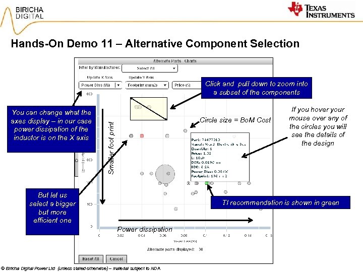
Hands-On Demo 11 – Alternative Component Selection Click and pull down to zoom into a subset of the components Circle size = Bo. M Cost Smaller foot print You can change what the axes display – in our case power dissipation of the inductor is on the X axis But let us select a bigger but more efficient one If you hover your mouse over any of the circles you will see the details of the design TI recommendation is shown in green Power dissipation © Biricha Digital Power Ltd (unless stated otherwise) – material subject to NDA
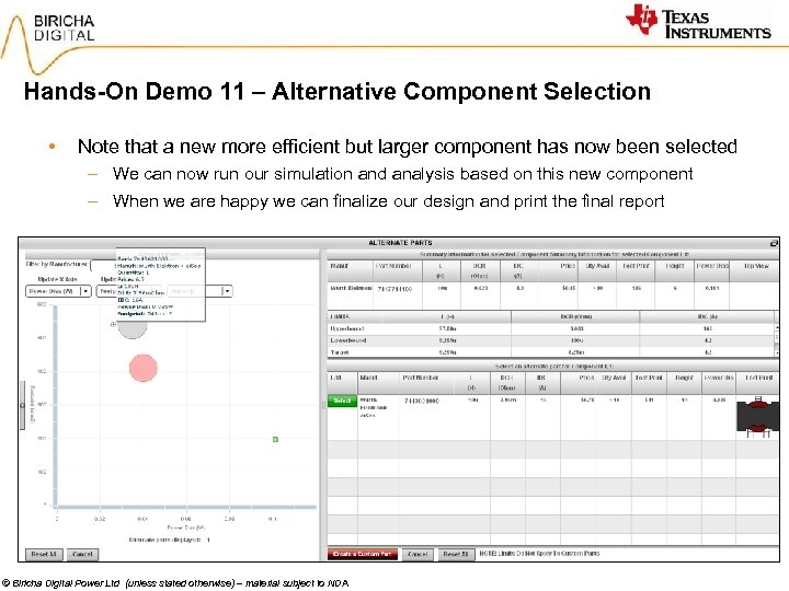
Hands-On Demo 11 – Alternative Component Selection • Note that a new more efficient but larger component has now been selected – We can now run our simulation and analysis based on this new component – When we are happy we can finalize our design and print the final report © Biricha Digital Power Ltd (unless stated otherwise) – material subject to NDA
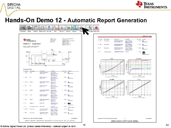
Hands-On Demo 12 - Automatic Report Generation © Biricha Digital Power Ltd (unless stated otherwise) – material subject to NDA 52 52
Concluding Remarks and Summary • WEBENCH is a very powerful tool to assist you in your Po. L PSU Designs – Based on your specifications, it automatically designs 100+ of PSUs • We’ve learned how to: – Filter down our designs and select the most appropriate part based on your efficiency/footprint/cost requirements – Optimize our design and carry out electrical and thermal simulations – Change components within your Bo. M – Create schematics and import to CAD packages – Print the final report and order Bo. M including the PCB within a few clicks • In this seminar we only covered Power Designer; there is also: – WEBENCH Power Architect – WEBENCH LED Designer – WEBENCH Sensor Designer – WEBENCH Active Filter Designer – WEBENCH Amplifier Designer – WEBENCH Easy. PLL © Biricha Digital Power Ltd (unless stated otherwise) – material subject to NDA www. ti. com/webench
© 2014 Texas Instruments Incorporated. The platform bar is a trademark of Texas Instruments. © Biricha Digital Power Ltd (unless stated otherwise) – material subject to NDA SNVP 003 54
f527c59c97b8e600154c9c2651787da6.ppt