92ddb72c05b3a3bbc3c9679690b7fa88.ppt
- Количество слайдов: 20
 Exploring the Rogue Wave Phenomenon in 3 D Power Distribution Networks Xiang Hu 1, Peng Du 2, Chung-Kuan Cheng 2 1 ECE Dept. , 2 CSE Dept. University of California, San Diego 10/25/2010
 Agenda Introduction System-level 3 D PDN analysis Chip-level 3 D PDN analysis – Detailed 3 D power grid model – Frequency-domain analysis – Time-domain analysis Conclusions Page 2
 Introduction Power delivery issues in 3 D ICs – Total currents flowing through off-chip components increase with the number of stacked tiers – 3 D-related components (i. e. , TSV, µbump) add more impedance to on-chip power grids Previous power grid models for on-chip noise analysis are relatively simple – Missed detailed metal layer information – Not suitable for 3 D PDN analysis Detailed 3 D PDN analysis has not been done – Frequency domain: resonance behavior – Time domain: worst-case noise Page 3
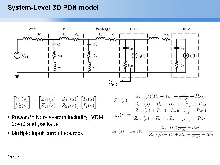 System-Level 3 D PDN model Zext Power delivery system including VRM, board and package Multiple input current sources Page 4
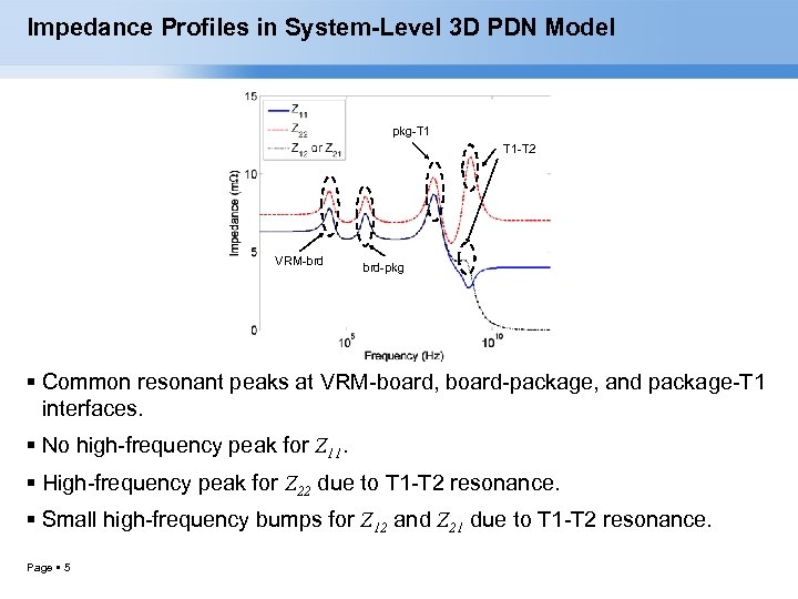 Impedance Profiles in System-Level 3 D PDN Model pkg-T 1 T 1 -T 2 VRM-brd brd-pkg Common resonant peaks at VRM-board, board-package, and package-T 1 interfaces. No high-frequency peak for Z 11. High-frequency peak for Z 22 due to T 1 -T 2 resonance. Small high-frequency bumps for Z 12 and Z 21 due to T 1 -T 2 resonance. Page 5
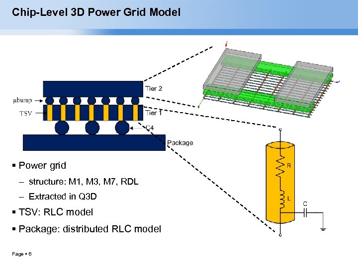 Chip-Level 3 D Power Grid Model Power grid – structure: M 1, M 3, M 7, RDL – Extracted in Q 3 D TSV: RLC model Package: distributed RLC model Page 6
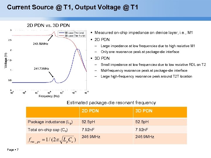 Current Source @ T 1, Output Voltage @ T 1 2 D PDN vs. 3 D PDN Measured on-chip impedance on device layer, i. e. , M 1 2 D PDN 243. 59 MHz – Large impedance at low frequencies due to high resistive M 1 – Only one resonance peak at package-die interface 3 D PDN – Small impedance at low frequencies due to low resistive RDL on T 2 – Mid-frequency resonance peak at package-die interface – 241. 73 MHz Large high-frequency resonance peak around T 2 T location Estimated package-die resonant frequency 2 D PDN Package inductance (Lp) 52. 5 p. H Total on-chip cap (Cc) 7. 92 n. F 246. 9 MHz Page 7 3 D PDN 246. 9 MHz
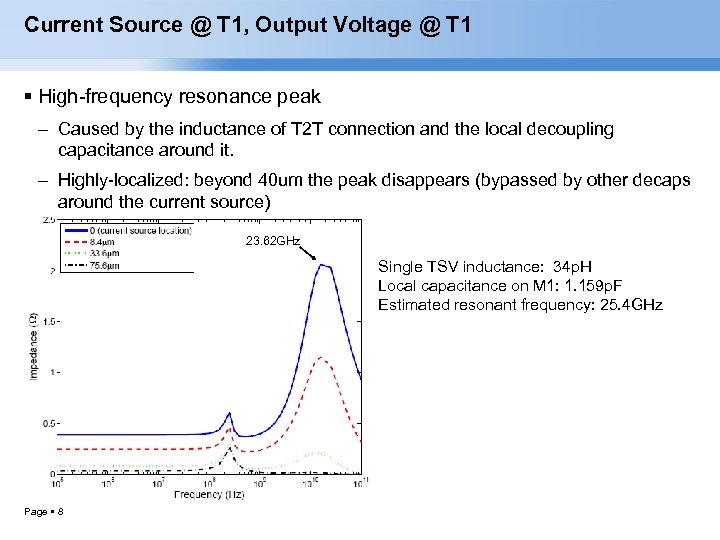 Current Source @ T 1, Output Voltage @ T 1 High-frequency resonance peak – Caused by the inductance of T 2 T connection and the local decoupling capacitance around it. – Highly-localized: beyond 40 um the peak disappears (bypassed by other decaps around the current source) 23. 62 GHz Single TSV inductance: 34 p. H Local capacitance on M 1: 1. 159 p. F Estimated resonant frequency: 25. 4 GHz Page 8
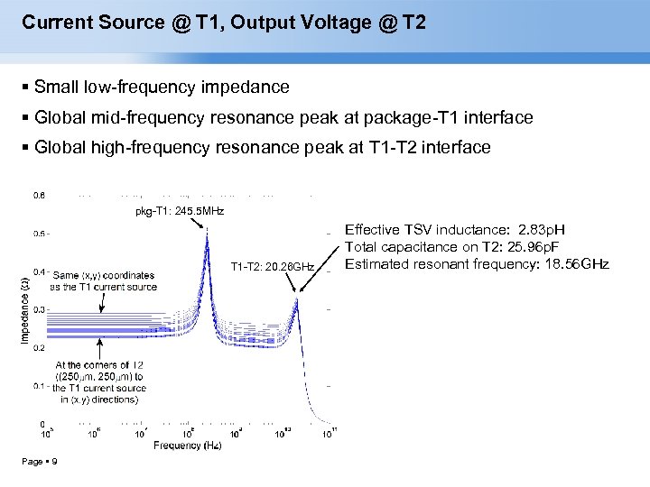 Current Source @ T 1, Output Voltage @ T 2 Small low-frequency impedance Global mid-frequency resonance peak at package-T 1 interface Global high-frequency resonance peak at T 1 -T 2 interface pkg-T 1: 245. 5 MHz T 1 -T 2: 20. 26 GHz Page 9 Effective TSV inductance: 2. 83 p. H Total capacitance on T 2: 25. 96 p. F Estimated resonant frequency: 18. 56 GHz
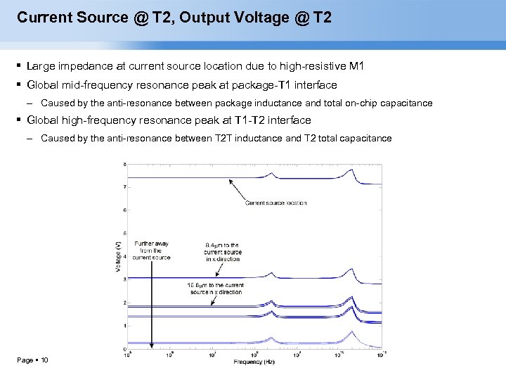 Current Source @ T 2, Output Voltage @ T 2 Large impedance at current source location due to high-resistive M 1 Global mid-frequency resonance peak at package-T 1 interface – Caused by the anti-resonance between package inductance and total on-chip capacitance Global high-frequency resonance peak at T 1 -T 2 interface – Caused by the anti-resonance between T 2 T inductance and T 2 total capacitance Page 10
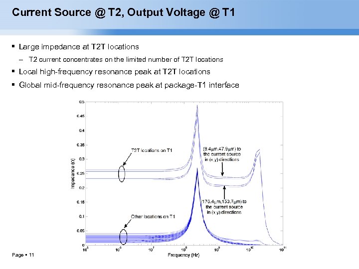 Current Source @ T 2, Output Voltage @ T 1 Large impedance at T 2 T locations – T 2 current concentrates on the limited number of T 2 T locations Local high-frequency resonance peak at T 2 T locations Global mid-frequency resonance peak at package-T 1 interface Page 11
 On-Chip Worst-Case PDN Noise Prediction Algorithm Motivation – Local current on M 1 is tiny consider the distributed current effect – Obtain worst-case noise at multiple on-chip locations Single-input worst-case PDN noise prediction algorithm [1] – Basic idea: dynamic programming Multi-input worst-case PDN noise prediction algorithm – Extension of the single-input algorithm – Based on noise superimposition of the linear PDN model [1] P. Du, X. Hu, S. H. Weng, A. Shayan, X. Chen, A. E. Engin, and C. K Cheng. “Worst-Case Noise Prediction With Non-Zero Current Transition Times for Early Power Distribution System Verification, ” In IEEE International Symposium on Quality Electronic Design, 2010 Page 12
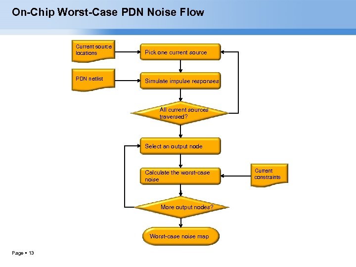 On-Chip Worst-Case PDN Noise Flow Current source locations Pick one current source PDN netlist Simulate impulse responses All current sources traversed? Select an output node Calculate the worst-case noise More output nodes? Worst-case noise map Page 13 Current constraints
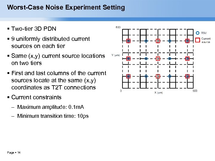 Worst-Case Noise Experiment Setting Two-tier 3 D PDN 9 uniformly distributed current sources on each tier Same (x, y) current source locations on two tiers First and last columns of the current sources locate at the same (x, y) coordinates as T 2 T connections Current constraints – Maximum amplitude: 0. 1 m. A – Minimum transition time: 10 ps Page 14
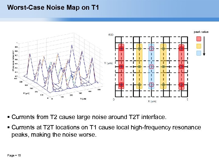 Worst-Case Noise Map on T 1 peak value Currents from T 2 cause large noise around T 2 T interface. Currents at T 2 T locations on T 1 cause local high-frequency resonance peaks, making the noise worse. Page 15
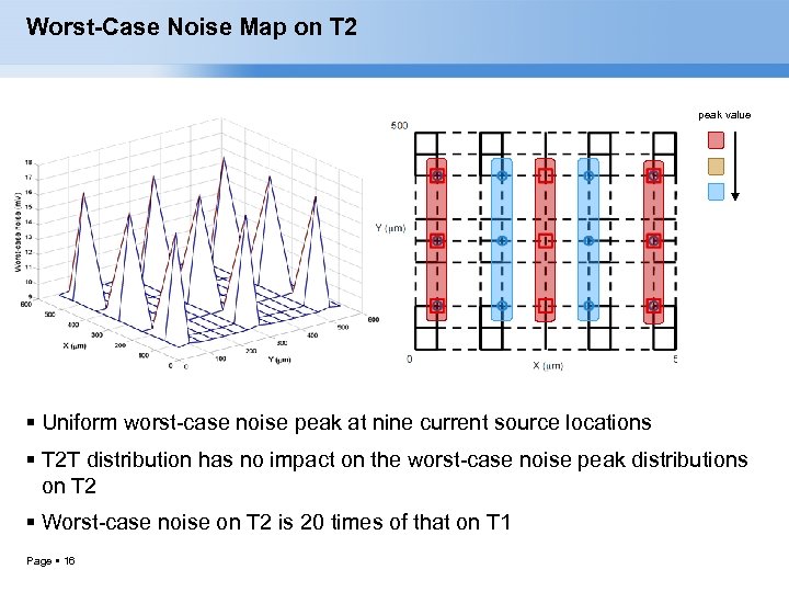 Worst-Case Noise Map on T 2 peak value Uniform worst-case noise peak at nine current source locations T 2 T distribution has no impact on the worst-case noise peak distributions on T 2 Worst-case noise on T 2 is 20 times of that on T 1 Page 16
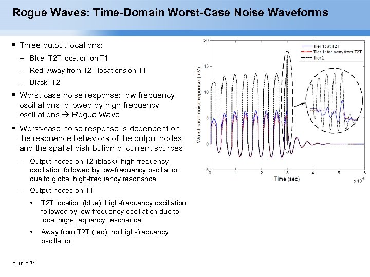 Rogue Waves: Time-Domain Worst-Case Noise Waveforms Three output locations: – Blue: T 2 T location on T 1 – Red: Away from T 2 T locations on T 1 – Black: T 2 Worst-case noise response: low-frequency oscillations followed by high-frequency oscillations Rogue Wave Worst-case noise response is dependent on the resonance behaviors of the output nodes and the spatial distribution of current sources – Output nodes on T 2 (black): high-frequency oscillation followed by low-frequency oscillation due to global high-frequency resonance – Output nodes on T 1 • T 2 T location (blue): high-frequency oscillation followed by low-frequency oscillation due to local high-frequency resonance • Away from T 2 T (red): no high-frequency oscillation Page 17
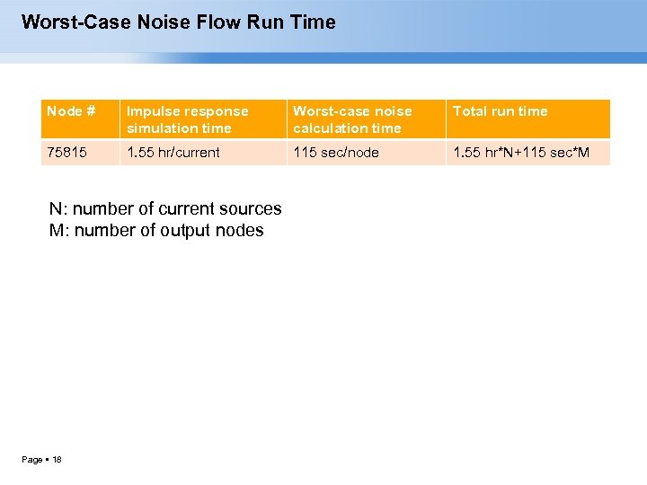 Worst-Case Noise Flow Run Time Node # Impulse response simulation time Worst-case noise calculation time Total run time 75815 1. 55 hr/current 115 sec/node 1. 55 hr*N+115 sec*M N: number of current sources M: number of output nodes Page 18
 Conclusions System-level analysis reveals the global resonance effects for 3 D PDNs Proposed on-chip 3 D power grid model with detailed metal layer Local resonance phenomenon due to T 2 T connection inductance and local capacitance is discovered with the detailed 3 D power grid model Worst-case noise calculation algorithm is extended to multiple input multiple output system Worst-case noise map shows the spatial distribution of the worst-case noise in 3 D PDNs The “rogue wave” of worst-case noise response reflects the resonance behaviors at different locations of the 3 D PDN Page 19
 Thank You! Q&A Page 20


