4335e54b3df1222177241ed1614bb1e7.ppt
- Количество слайдов: 40

Experiences with Two Fab. Scalar-based Chips Elliott Forbes, Rangeen Basu Roy Chowdhury, Brandon Dwiel, Anil Kannepalli, Vinesh Srinivasan, Zhenqian Zhang, Randy Widialaksono, Thomas Belanger, Steve Lipa, Eric Rotenberg, W. Rhett Davis, Paul D. Franzon Electrical and Computer Engineering – North Carolina State University
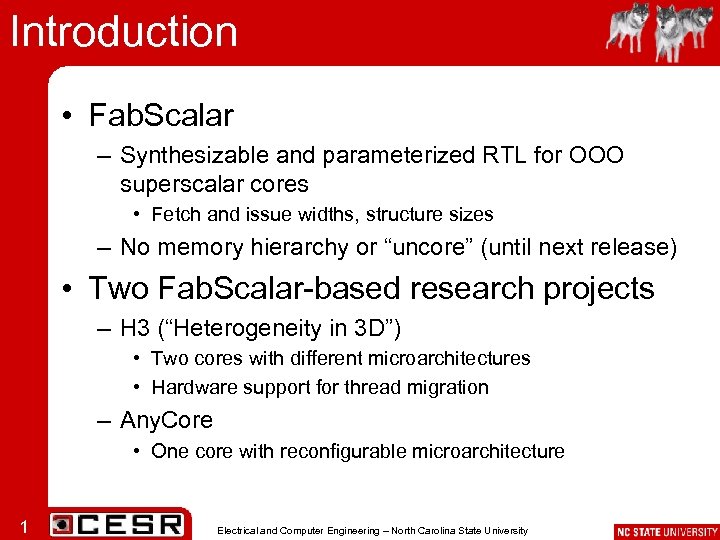
Introduction • Fab. Scalar – Synthesizable and parameterized RTL for OOO superscalar cores • Fetch and issue widths, structure sizes – No memory hierarchy or “uncore” (until next release) • Two Fab. Scalar-based research projects – H 3 (“Heterogeneity in 3 D”) • Two cores with different microarchitectures • Hardware support for thread migration – Any. Core • One core with reconfigurable microarchitecture 1 Electrical and Computer Engineering – North Carolina State University
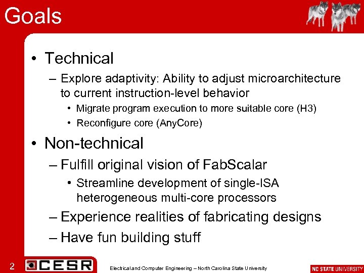
Goals • Technical – Explore adaptivity: Ability to adjust microarchitecture to current instruction-level behavior • Migrate program execution to more suitable core (H 3) • Reconfigure core (Any. Core) • Non-technical – Fulfill original vision of Fab. Scalar • Streamline development of single-ISA heterogeneous multi-core processors – Experience realities of fabricating designs – Have fun building stuff 2 Electrical and Computer Engineering – North Carolina State University
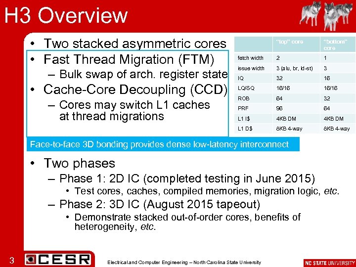
H 3 Overview • Two stacked asymmetric cores • Fast Thread Migration (FTM) • Cache-Core Decoupling (CCD) – Cores may switch L 1 caches at thread migrations “bottom” core fetch width 2 1 issue width 3 (alu, br, ld-st) 3 IQ 32 16 LQ/SQ 16/16 ROB 64 32 PRF 96 64 L 1 I$ 4 KB DM L 1 D$ – Bulk swap of arch. register state “top” core 8 KB 4 -way Face-to-face 3 D bonding provides dense low-latency interconnect • Two phases – Phase 1: 2 D IC (completed testing in June 2015) • Test cores, caches, compiled memories, migration logic, etc. – Phase 2: 3 D IC (August 2015 tapeout) • Demonstrate stacked out-of-order cores, benefits of heterogeneity, etc. 3 Electrical and Computer Engineering – North Carolina State University
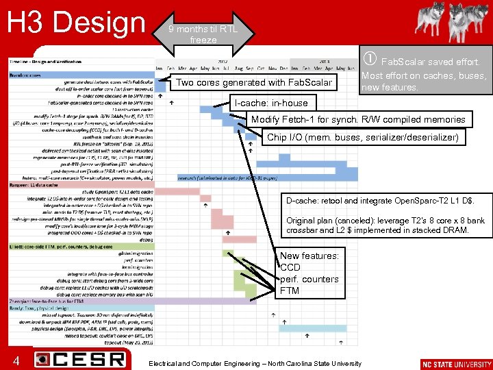
H 3 Design 9 months til RTL freeze Fab. Scalar saved effort. Two cores generated with Fab. Scalar Most effort on caches, buses, new features. I-cache: in-house Modify Fetch-1 for synch. R/W compiled memories Chip I/O (mem. buses, serializer/deserializer) D-cache: retool and integrate Open. Sparc-T 2 L 1 D$. Original plan (canceled): leverage T 2’s 8 core x 8 bank crossbar and L 2 $ implemented in stacked DRAM. New features: CCD perf. counters FTM 4 Electrical and Computer Engineering – North Carolina State University
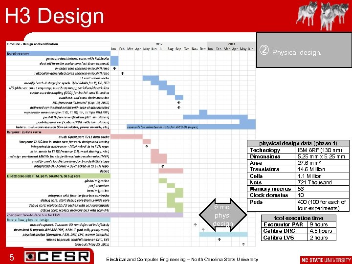
H 3 Design Physical design. 6 mo. phys. design 5 physical design data (phase 1) Technology IBM 8 RF (130 nm) Dimensions 5. 25 mm x 5. 25 mm Area 27. 6 mm 2 Transistors 14. 6 Million Cells 1. 1 Million Nets 721 Thousand Memory macros 56 Clock domains 10 Pads 400 (100 for each of four experiments) Electrical and Computer Engineering – North Carolina State University tool execution time Encounter PAR 9 hours Calibre DRC 4. 5 hours Calibre LVS 2 hours
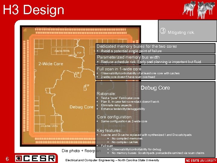
H 3 Design Mitigating risk. Dedicated memory buses for the two cores • Avoid a potential single point of failure Parameterized memory bus width • Reduce schedule risk: Early pad planning is important but fluid. Full scan in 1 -wide core • Observability/controllability of at least one core with caches • 2 -wide core doesn’t have scan overhead Debug Core Rationale: • • Test a “pure” Fab. Scalar core Plan B, in case two-core-stack doesn’t work Eliminate risky aspects Enhance testability/debuggability Core configuration: • Same configuration as 2 -wide core Key features: • I-cache and D-cache replaced with synthesized I and D scratchpads • No compiled memories • No complex caches • Full scan • Observability/controllability for debug Die photo + floorplan • No memory buses: Scratchpads preloaded/examined via scan chains 6 Electrical and Computer Engineering – North Carolina State University
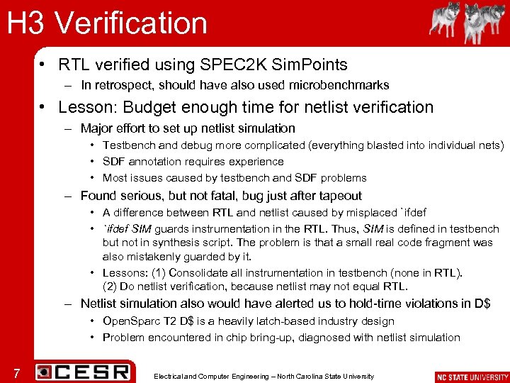
H 3 Verification • RTL verified using SPEC 2 K Sim. Points – In retrospect, should have also used microbenchmarks • Lesson: Budget enough time for netlist verification – Major effort to set up netlist simulation • Testbench and debug more complicated (everything blasted into individual nets) • SDF annotation requires experience • Most issues caused by testbench and SDF problems – Found serious, but not fatal, bug just after tapeout • A difference between RTL and netlist caused by misplaced `ifdef • `ifdef SIM guards instrumentation in the RTL. Thus, SIM is defined in testbench but not in synthesis script. The problem is that a small real code fragment was also mistakenly guarded by it. • Lessons: (1) Consolidate all instrumentation in testbench (none in RTL). (2) Do netlist verification, because netlist may not equal RTL. – Netlist simulation also would have alerted us to hold-time violations in D$ • Open. Sparc T 2 D$ is a heavily latch-based industry design • Problem encountered in chip bring-up, diagnosed with netlist simulation 7 Electrical and Computer Engineering – North Carolina State University
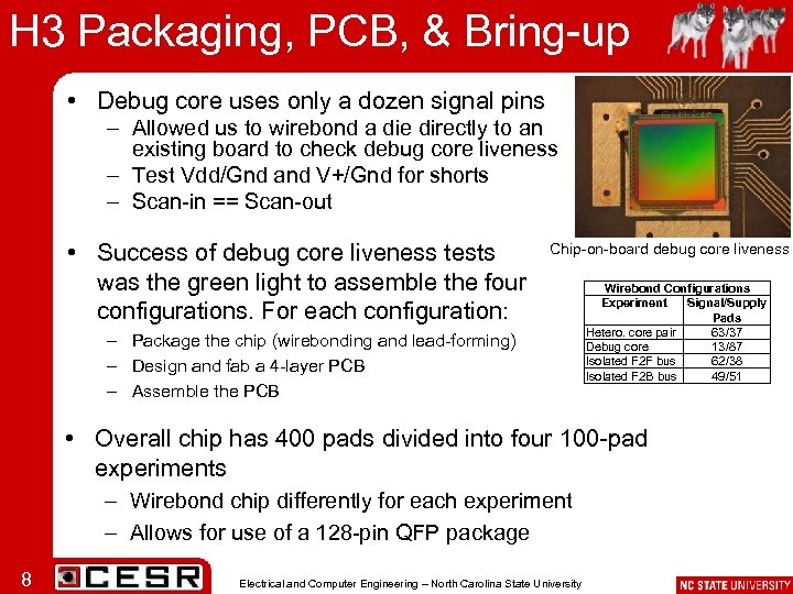
H 3 Packaging, PCB, & Bring-up • Debug core uses only a dozen signal pins – Allowed us to wirebond a die directly to an existing board to check debug core liveness – Test Vdd/Gnd and V+/Gnd for shorts – Scan-in == Scan-out • Success of debug core liveness tests was the green light to assemble the four configurations. For each configuration: Chip-on-board debug core liveness – Package the chip (wirebonding and lead-forming) – Design and fab a 4 -layer PCB – Assemble the PCB Wirebond Configurations Experiment Signal/Supply Pads Hetero. core pair 63/37 Debug core 13/87 Isolated F 2 F bus 62/38 Isolated F 2 B bus 49/51 • Overall chip has 400 pads divided into four 100 -pad experiments – Wirebond chip differently for each experiment – Allows for use of a 128 -pin QFP package 8 Electrical and Computer Engineering – North Carolina State University
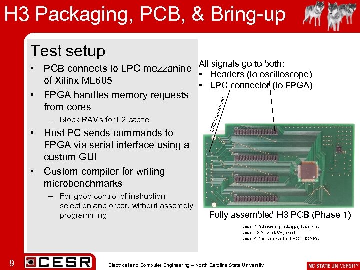
H 3 Packaging, PCB, & Bring-up Test setup All signals go to both: • Host PC sends commands to FPGA via serial interface using a custom GUI • Custom compiler for writing microbenchmarks – For good control of instruction selection and order, without assembly programming LPC – Block RAMs for L 2 cache und erne ath • PCB connects to LPC mezzanine • Headers (to oscilloscope) of Xilinx ML 605 • LPC connector (to FPGA) • FPGA handles memory requests from cores Fully assembled H 3 PCB (Phase 1) Layer 1 (shown): package, headers Layers 2, 3: Vdd/V+, Gnd Layer 4 (underneath): LPC, DCAPs 9 Electrical and Computer Engineering – North Carolina State University
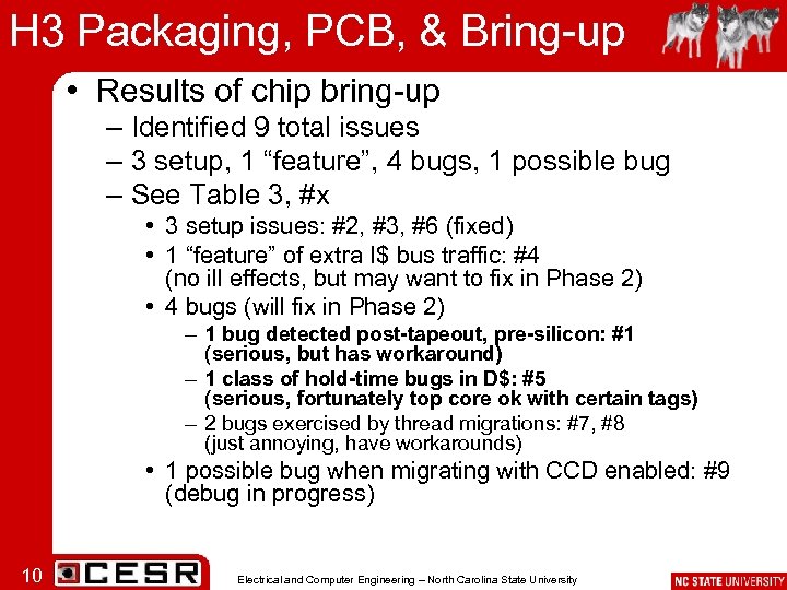
H 3 Packaging, PCB, & Bring-up • Results of chip bring-up – Identified 9 total issues – 3 setup, 1 “feature”, 4 bugs, 1 possible bug – See Table 3, #x • 3 setup issues: #2, #3, #6 (fixed) • 1 “feature” of extra I$ bus traffic: #4 (no ill effects, but may want to fix in Phase 2) • 4 bugs (will fix in Phase 2) – 1 bug detected post-tapeout, pre-silicon: #1 (serious, but has workaround) – 1 class of hold-time bugs in D$: #5 (serious, fortunately top core ok with certain tags) – 2 bugs exercised by thread migrations: #7, #8 (just annoying, have workarounds) • 1 possible bug when migrating with CCD enabled: #9 (debug in progress) 10 Electrical and Computer Engineering – North Carolina State University
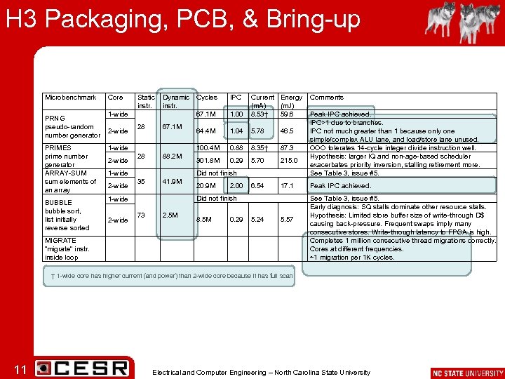
H 3 Packaging, PCB, & Bring-up Microbenchmark PRNG pseudo-random number generator Core 1 -wide 2 -wide PRIMES prime number generator ARRAY-SUM sum elements of an array Did not finish 28 67. 1 M 28 88. 2 M 35 41. 9 M 1 -wide MIGRATE “migrate” instr. inside loop 2 -wide 1 -wide 2 -wide IPC Current Energy Comments (m. A) (m. J) 8. 53† 59. 6 Peak IPC achieved. IPC>1 due to branches. 5. 78 46. 5 IPC not much greater than 1 because only one simple/complex ALU lane, and load/store lane unused. 8. 35† 87. 3 OOO tolerates 14 -cycle integer divide instruction well. Hypothesis: larger IQ and non-age-based scheduler 5. 70 215. 0 exacerbates priority inversion, stalling retirement more. See Table 3, issue #5. 20. 9 M 6. 54 1. 00 64. 4 M 1. 04 100. 4 M 1 -wide BUBBLE bubble sort, list initially reverse sorted Static Dynamic Cycles instr. 67. 1 M 0. 88 301. 8 M 0. 29 2. 00 17. 1 Did not finish 73 2. 5 M 8. 5 M 0. 29 5. 24 5. 57 Peak IPC achieved. See Table 3, issue #5. Early diagnosis: SQ stalls dominate other resource stalls. Hypothesis: Limited store buffer size of write-through D$ causing back-pressure. Frequent swaps imply many consecutive stores. Write-through latency to FPGA is high. Completes 1 million consecutive thread migrations correctly. Cores at different frequencies. ~1 migration per 1 K cycles. † 1 -wide core has higher current (and power) than 2 -wide core because it has full scan. 11 Electrical and Computer Engineering – North Carolina State University
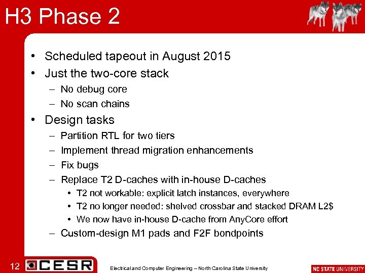
H 3 Phase 2 • Scheduled tapeout in August 2015 • Just the two-core stack – No debug core – No scan chains • Design tasks – – Partition RTL for two tiers Implement thread migration enhancements Fix bugs Replace T 2 D-caches with in-house D-caches • T 2 not workable: explicit latch instances, everywhere • T 2 no longer needed: shelved crossbar and stacked DRAM L 2$ • We now have in-house D-cache from Any. Core effort – Custom-design M 1 pads and F 2 F bondpoints 12 Electrical and Computer Engineering – North Carolina State University
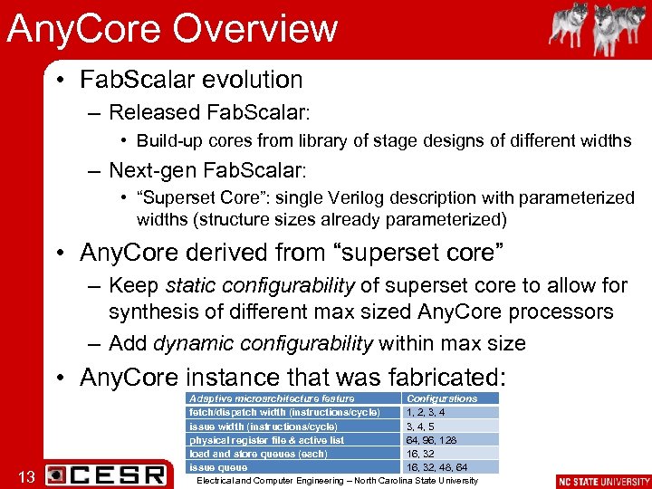
Any. Core Overview • Fab. Scalar evolution – Released Fab. Scalar: • Build-up cores from library of stage designs of different widths – Next-gen Fab. Scalar: • “Superset Core”: single Verilog description with parameterized widths (structure sizes already parameterized) • Any. Core derived from “superset core” – Keep static configurability of superset core to allow for synthesis of different max sized Any. Core processors – Add dynamic configurability within max size • Any. Core instance that was fabricated: 13 Adaptive microarchitecture feature fetch/dispatch width (instructions/cycle) issue width (instructions/cycle) physical register file & active list load and store queues (each) issue queue Configurations 1, 2, 3, 4, 5 64, 96, 128 16, 32, 48, 64 Electrical and Computer Engineering – North Carolina State University
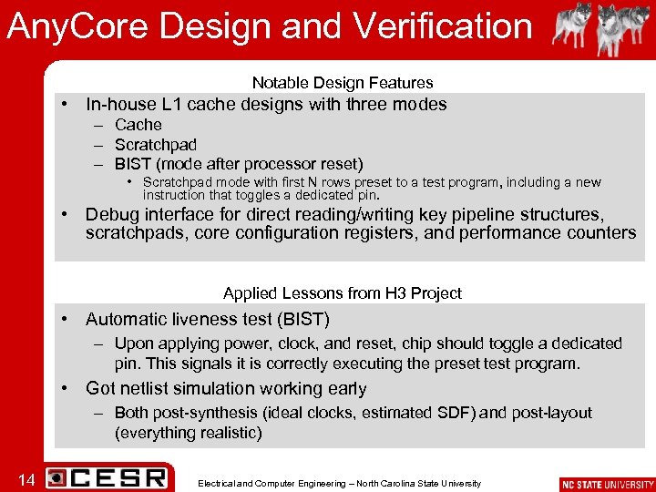
Any. Core Design and Verification Notable Design Features • In-house L 1 cache designs with three modes – Cache – Scratchpad – BIST (mode after processor reset) • Scratchpad mode with first N rows preset to a test program, including a new instruction that toggles a dedicated pin. • Debug interface for direct reading/writing key pipeline structures, scratchpads, core configuration registers, and performance counters Applied Lessons from H 3 Project • Automatic liveness test (BIST) – Upon applying power, clock, and reset, chip should toggle a dedicated pin. This signals it is correctly executing the preset test program. • Got netlist simulation working early – Both post-synthesis (ideal clocks, estimated SDF) and post-layout (everything realistic) 14 Electrical and Computer Engineering – North Carolina State University
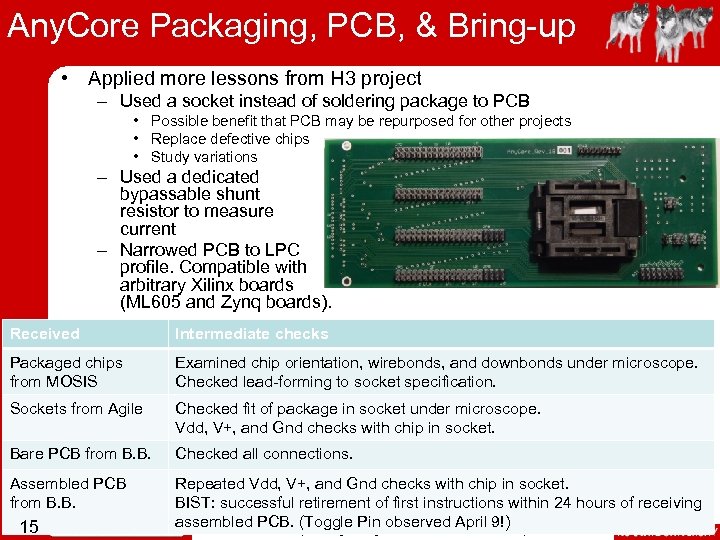
Any. Core Packaging, PCB, & Bring-up • Applied more lessons from H 3 project – Used a socket instead of soldering package to PCB • Possible benefit that PCB may be repurposed for other projects • Replace defective chips • Study variations – Used a dedicated bypassable shunt resistor to measure current – Narrowed PCB to LPC profile. Compatible with arbitrary Xilinx boards (ML 605 and Zynq boards). Received Intermediate checks Packaged chips from MOSIS Examined chip orientation, wirebonds, and downbonds under microscope. Checked lead-forming to socket specification. Sockets from Agile Checked fit of package in socket under microscope. Vdd, V+, and Gnd checks with chip in socket. Bare PCB from B. B. Checked all connections. Assembled PCB from B. B. Repeated Vdd, V+, and Gnd checks with chip in socket. BIST: successful retirement of first instructions within 24 hours of receiving assembled PCB. (Toggle Pin observed April 9!) Electrical and Computer Engineering – North Carolina State University 15
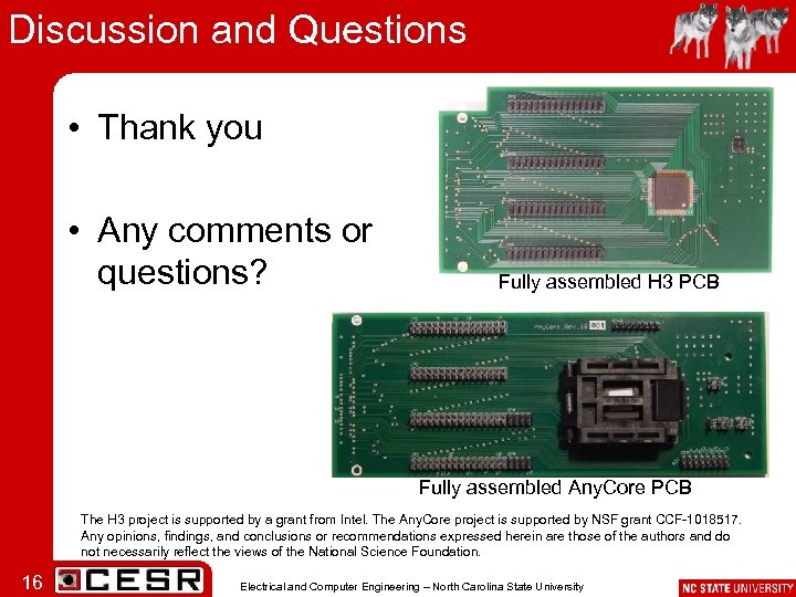
Discussion and Questions • Thank you • Any comments or questions? Fully assembled H 3 PCB Fully assembled Any. Core PCB The H 3 project is supported by a grant from Intel. The Any. Core project is supported by NSF grant CCF-1018517. Any opinions, findings, and conclusions or recommendations expressed herein are those of the authors and do not necessarily reflect the views of the National Science Foundation. 16 Electrical and Computer Engineering – North Carolina State University

Backup Electrical and Computer Engineering – North Carolina State University
References N. K. Choudhary, S. V. Wadhavkar, T. A. Shah, H. Mayukh, J. Gandhi, B. H. Dwiel, S. Navada, H. H. Najaf-abadi, and E. Rotenberg. Fab. Scalar: Composing Synthesizable RTL Designs of Arbitrary Cores within a Canonical Superscalar Template. Proceedings of the 38 th IEEE/ACM International Symposium on Computer Architecture (ISCA-38), pp. 11 -22, June 2011. E. Rotenberg, B. Dwiel, E. Forbes, Z. Zhang, R. Widialaksono, R. Basu Roy Chowdhury, N. Tshibangu, S. Lipa, W. R. Davis, and P. D. Franzon. Rationale for a 3 D Heterogeneous Multi-core Processor. Proceedings of the 31 st IEEE International Conference on Computer Design (ICCD-31), pp. 154 -168, October 2013. Electrical and Computer Engineering – North Carolina State University
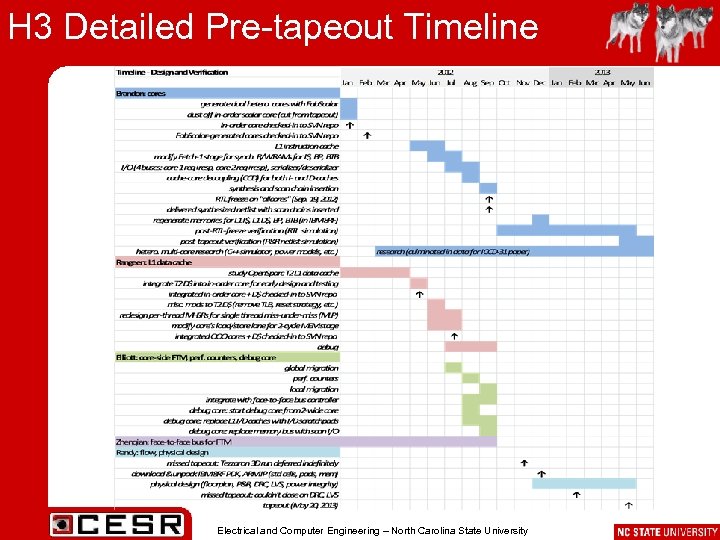
H 3 Detailed Pre-tapeout Timeline Electrical and Computer Engineering – North Carolina State University
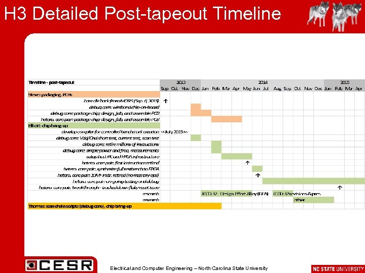
H 3 Detailed Post-tapeout Timeline Electrical and Computer Engineering – North Carolina State University
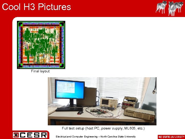
Cool H 3 Pictures Final layout Full test setup (host PC, power supply, ML 605, etc. ) Electrical and Computer Engineering – North Carolina State University
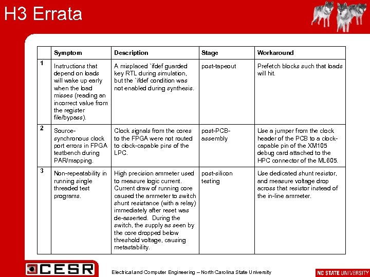
H 3 Errata Symptom Description Stage Workaround 1 Instructions that depend on loads will wake up early when the load misses (reading an incorrect value from the register file/bypass). A misplaced `ifdef guarded key RTL during simulation, but the `ifdef condition was not enabled during synthesis. post-tapeout Prefetch blocks such that loads will hit. 2 Sourcesynchronous clock port errors in FPGA testbench during PAR/mapping. Clock signals from the cores to the FPGA were not routed to clock-capable pins of the LPC. post-PCBassembly Use a jumper from the clock header of the PCB to a clockcapable pin of the XM 105 debug card attached to the HPC connector of the ML 605. 3 Non-repeatability in running single threaded test programs. High precision ammeter used post-silicon to measure logic current. testing Current draw of running core caused the ammeter to switch shunt resistance (with a relay) immediately after reset was de-asserted. During the switch, the supply as seen by the core dropped below threshold voltage, causing metastability. Use dedicated shunt resistor, and measure voltage drop across that resistor instead of the in-line ammeter. Electrical and Computer Engineering – North Carolina State University
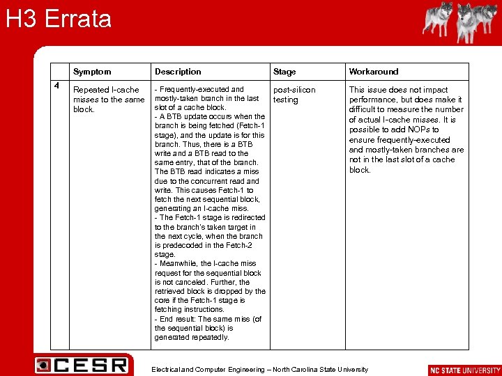
H 3 Errata Symptom 4 - Frequently-executed and Repeated I-cache misses to the same mostly-taken branch in the last slot of a cache block. Description - A BTB update occurs when the branch is being fetched (Fetch-1 stage), and the update is for this branch. Thus, there is a BTB write and a BTB read to the same entry, that of the branch. The BTB read indicates a miss due to the concurrent read and write. This causes Fetch-1 to fetch the next sequential block, generating an I-cache miss. - The Fetch-1 stage is redirected to the branch’s taken target in the next cycle, when the branch is predecoded in the Fetch-2 stage. - Meanwhile, the I-cache miss request for the sequential block is not canceled. Further, the retrieved block is dropped by the core if the Fetch-1 stage is fetching instructions. - End result: The same miss (of the sequential block) is generated repeatedly. Stage Workaround post-silicon testing This issue does not impact performance, but does make it difficult to measure the number of actual I-cache misses. It is possible to add NOPs to ensure frequently-executed and mostly-taken branches are not in the last slot of a cache block. Electrical and Computer Engineering – North Carolina State University
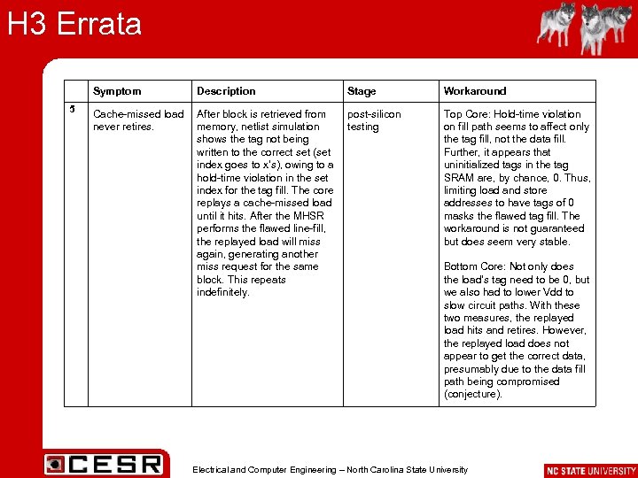
H 3 Errata Symptom 5 Cache-missed load After block is retrieved from never retires. memory, netlist simulation shows the tag not being written to the correct set (set index goes to x’s), owing to a hold-time violation in the set index for the tag fill. The core replays a cache-missed load until it hits. After the MHSR performs the flawed line-fill, the replayed load will miss again, generating another miss request for the same block. This repeats indefinitely. Description Stage Workaround post-silicon testing Top Core: Hold-time violation on fill path seems to affect only the tag fill, not the data fill. Further, it appears that uninitialized tags in the tag SRAM are, by chance, 0. Thus, limiting load and store addresses to have tags of 0 masks the flawed tag fill. The workaround is not guaranteed but does seem very stable. Bottom Core: Not only does the load’s tag need to be 0, but we also had to lower Vdd to slow circuit paths. With these two measures, the replayed load hits and retires. However, the replayed load does not appear to get the correct data, presumably due to the data fill path being compromised (conjecture). Electrical and Computer Engineering – North Carolina State University
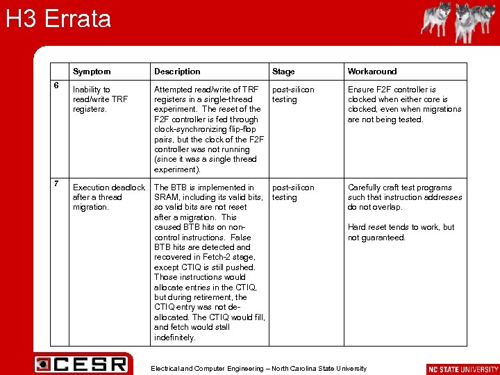
H 3 Errata Symptom Description 6 Inability to read/write TRF registers. Attempted read/write of TRF post-silicon registers in a single-thread testing experiment. The reset of the F 2 F controller is fed through clock-synchronizing flip-flop pairs, but the clock of the F 2 F controller was not running (since it was a single thread experiment). Ensure F 2 F controller is clocked when either core is clocked, even when migrations are not being tested. 7 Execution deadlock The BTB is implemented in post-silicon after a thread SRAM, including its valid bits, testing migration. so valid bits are not reset after a migration. This caused BTB hits on noncontrol instructions. False BTB hits are detected and recovered in Fetch-2 stage, except CTIQ is still pushed. Those instructions would allocate entries in the CTIQ, but during retirement, the CTIQ entry was not deallocated. The CTIQ would fill, and fetch would stall indefinitely. Carefully craft test programs such that instruction addresses do not overlap. Hard reset tends to work, but not guaranteed. Stage Workaround Electrical and Computer Engineering – North Carolina State University
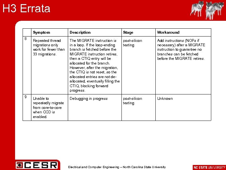
H 3 Errata Symptom Description 8 Repeated thread migrations only work for fewer than 33 migrations. The MIGRATE instruction is post-silicon in a loop. If the loop-ending testing branch is fetched before the MIGRATE instruction retires, then a CTIQ entry will be allocated for the branch. However, after the migration, the CTIQ is not reset, so the allocated entries are not deallocated, eventually filling the CTIQ, blocking forward progress. Add instructions (NOPs if necessary) after a MIGRATE instruction to guarantee no branches can be fetched before the MIGRATE retires. 9 Unable to repeatedly migrate from core-to-core when CCD is enabled. Debugging in progress Unknown Stage post-silicon testing Workaround Electrical and Computer Engineering – North Carolina State University
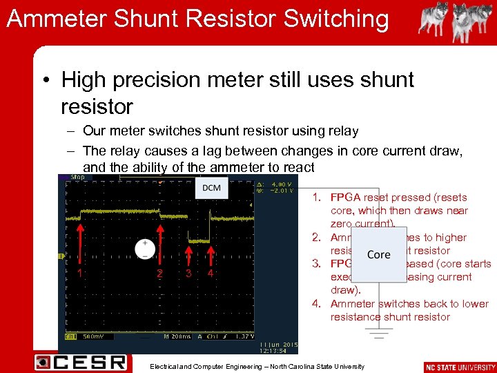
Ammeter Shunt Resistor Switching • High precision meter still uses shunt resistor – Our meter switches shunt resistor using relay – The relay causes a lag between changes in core current draw, and the ability of the ammeter to react 1 2 3 4 1. FPGA reset pressed (resets core, which then draws near zero current). 2. Ammeter switches to higher resistance shunt resistor 3. FPGA reset released (core starts executing, increasing current draw). 4. Ammeter switches back to lower resistance shunt resistor Electrical and Computer Engineering – North Carolina State University
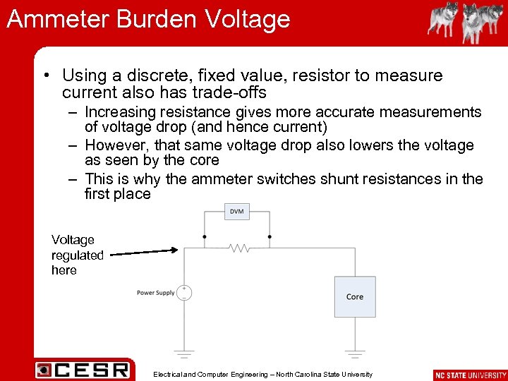
Ammeter Burden Voltage • Using a discrete, fixed value, resistor to measure current also has trade-offs – Increasing resistance gives more accurate measurements of voltage drop (and hence current) – However, that same voltage drop also lowers the voltage as seen by the core – This is why the ammeter switches shunt resistances in the first place Voltage regulated here Electrical and Computer Engineering – North Carolina State University
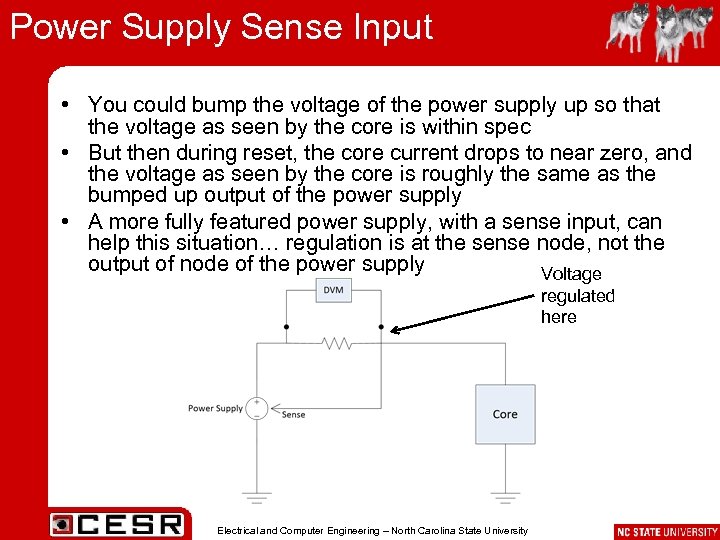
Power Supply Sense Input • You could bump the voltage of the power supply up so that the voltage as seen by the core is within spec • But then during reset, the core current drops to near zero, and the voltage as seen by the core is roughly the same as the bumped up output of the power supply • A more fully featured power supply, with a sense input, can help this situation… regulation is at the sense node, not the output of node of the power supply Voltage regulated here Electrical and Computer Engineering – North Carolina State University
Custom Compiler • Needed a way to explicitly control all aspects of emitted instructions • Language syntax is assembly with a few higher-level features – Registers and memory locations can be named – if statements and while loops – Arithmetic operators, assignments, address-of • Syntax allows the ability to place code/data at arbitrary memory locations – Including non-contiguous locations • The compiler also emits to our checkpoint file format • Written in flex/bison Electrical and Computer Engineering – North Carolina State University
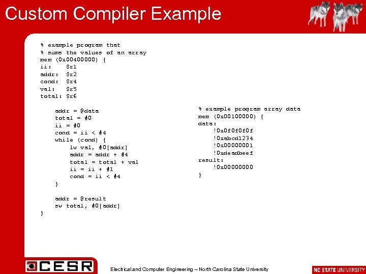
Custom Compiler Example % example program that % sums the values of an array mem (0 x 00400000) { ii: $r 1 addr: $r 2 cond: $r 4 val: $r 5 total: $r 6 addr = @data total = #0 ii = #0 cond = ii < #4 while (cond) { lw val, #0[addr] addr = addr + #4 total = total + val ii = ii + #1 cond = ii < #4 } % example program array data mem (0 x 00100000) { data: !0 x 0 f 0 f !0 xabcd 1234 !0 x 00000001 !0 xdeadbeef result: !0 x 0000 } addr = @result sw total, #0[addr] } Electrical and Computer Engineering – North Carolina State University
Intel 80386 Errata (it’s not just us!) • Hardware Peculiarity: Unless pin F 13 of the 80386 is connected to the +5 V power supply, the 80386 never terminates a memory cycle, halting the processor. – Datasheet indicates pin F 13 is NC with a note that “Pins identified as ‘NC’ should remain completely unconnected. ” • Successive Floating-Point Instructions: If two floating-point instructions are executed close together, the 80386 may force the coprocessor to start the second one too soon if the first one did not require any memory operands. • Misaligned Floating-Point Instructions: If 80287 and/or 80387 instructions are not word-aligned, the 80386 passes the wrong instruction to the coprocessor, causing unpredictable behavior. • Self-test: The self-test feature does not work on the A 1 stepping of the 80386. • Double Page Faults: The bug that appeared in the B 0 stepping regarding page faults that occur during page faults has been made a permanent feature of the 80386… Turley, James L. , Advanced 80386 Programming Techniques, Mc. Graw-Hill, Berkeley, CA, 1988. Electrical and Computer Engineering – North Carolina State University
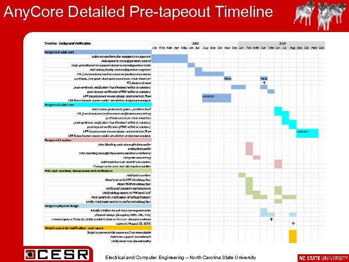
Any. Core Detailed Pre-tapeout Timeline Electrical and Computer Engineering – North Carolina State University
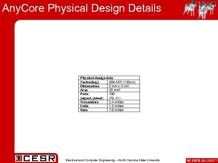
Any. Core Physical Design Details Physical design data Technology IBM 8 RF (130 nm) Dimensions 5 mm x 5 mm Area 25 mm 2 Pads 100 (signal, power) (79, 21) Transistors 3. 4 million Cells 1. 5 million Nets 7. 6 million Electrical and Computer Engineering – North Carolina State University
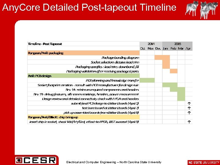
Any. Core Detailed Post-tapeout Timeline Electrical and Computer Engineering – North Carolina State University
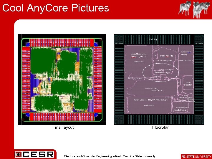
Cool Any. Core Pictures Final layout Floorplan Electrical and Computer Engineering – North Carolina State University
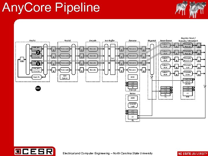
Any. Core Pipeline Electrical and Computer Engineering – North Carolina State University
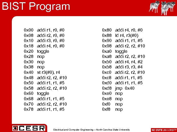
BIST Program 0 x 00 addi r 1, r 0, #0 0 x 08 addi r 2, r 0, #0 0 x 10 addi r 3, r 0, #0 0 x 18 addi r 4, r 0, #0 0 x 20 toggle 0 x 28 nop 0 x 30 nop 0 x 38 nop 0 x 40 st r 3(#0), r 4 0 x 48 addi r 2, #10 0 x 50 addi r 1, #5 0 x 58 addi r 2, #10 0 x 60 toggle 0 x 68 addi r 1, #5 0 x 70 addi r 2, #10 0 x 78 addi r 1, #5 0 x 80 addi r 4, r 0, #0 0 x 88 ld r 4, r 3(#0) 0 x 90 addi r 1, #5 0 x 98 addi r 2, #10 0 xa 0 toggle 0 xa 8 addi r 2, #10 0 xb 0 addi r 4, #2 0 xb 8 addi r 3, #4 0 xc 0 addi r 2, #10 0 xc 8 addi r 1, #5 0 xd 0 addi r 1, #5 0 xd 8 jmp 0 x 40 0 xe 0 nop 0 xe 8 nop 0 xf 0 nop 0 xf 8 nop Electrical and Computer Engineering – North Carolina State University
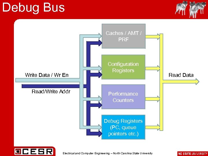
Debug Bus Caches / AMT / PRF Write Data / Wr En Read/Write Addr Configuration Registers Performance Counters Debug Registers (PC, queue pointers etc. ) Electrical and Computer Engineering – North Carolina State University Read Data
4335e54b3df1222177241ed1614bb1e7.ppt