d5ee4d57934c8b27dda779e6012592cc.ppt
- Количество слайдов: 52
 EQUIPE SYSTEMES DE COMMUNICATION ET MICROSYSTEMES : ESYCOM / EA 2552 COMMUNICATION SYSTEMS AND MEMS TEAM C. Rumelhard
 SUMMARY 1 – Origin of ESYCOM 2 – Configuration of ESYCOM 3 – An example of item: Microwave Photonics 4 – Synthesis and prospects ESYCOM 5 avril 2005 C. R. 2
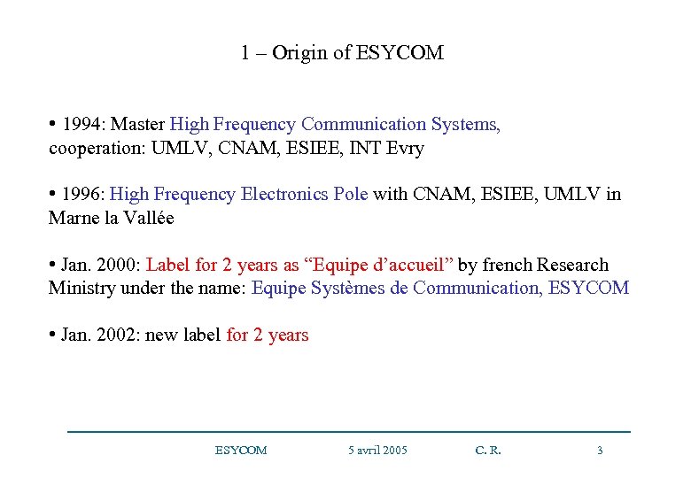 1 – Origin of ESYCOM • 1994: Master High Frequency Communication Systems, cooperation: UMLV, CNAM, ESIEE, INT Evry • 1996: High Frequency Electronics Pole with CNAM, ESIEE, UMLV in Marne la Vallée • Jan. 2000: Label for 2 years as “Equipe d’accueil” by french Research Ministry under the name: Equipe Systèmes de Communication, ESYCOM • Jan. 2002: new label for 2 years ESYCOM 5 avril 2005 C. R. 3
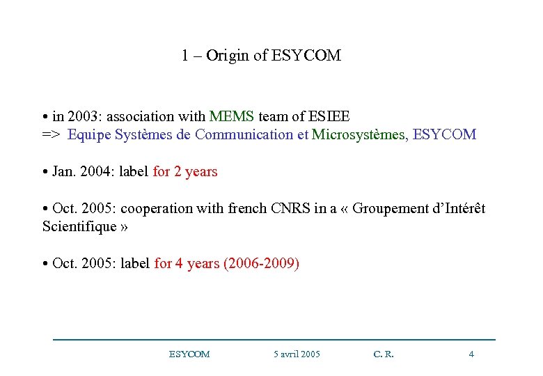 1 – Origin of ESYCOM • in 2003: association with MEMS team of ESIEE => Equipe Systèmes de Communication et Microsystèmes, ESYCOM • Jan. 2004: label for 2 years • Oct. 2005: cooperation with french CNRS in a « Groupement d’Intérêt Scientifique » • Oct. 2005: label for 4 years (2006 -2009) ESYCOM 5 avril 2005 C. R. 4
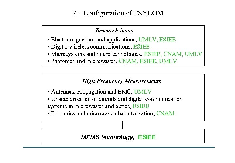 2 – Configuration of ESYCOM Research items • Electromagnetism and applications, UMLV, ESIEE • Digital wireless communications, ESIEE • Microsystems and microtechnologies, ESIEE, CNAM, UMLV • Photonics and microwaves, CNAM, ESIEE, UMLV High Frequency Measurements • Antennas, Propagation and EMC, UMLV • Characterisation of circuits and digital communication systems in microwaves and optics, ESIEE • Photonics and microwave characterisation, CNAM MEMS technology, ESIEE
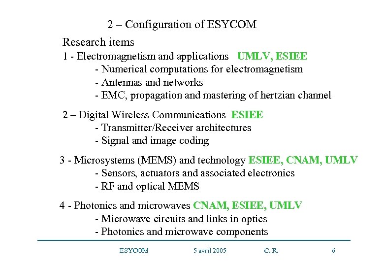 2 – Configuration of ESYCOM Research items 1 - Electromagnetism and applications UMLV, ESIEE - Numerical computations for electromagnetism - Antennas and networks - EMC, propagation and mastering of hertzian channel 2 – Digital Wireless Communications ESIEE - Transmitter/Receiver architectures - Signal and image coding 3 - Microsystems (MEMS) and technology ESIEE, CNAM, UMLV - Sensors, actuators and associated electronics - RF and optical MEMS 4 - Photonics and microwaves CNAM, ESIEE, UMLV - Microwave circuits and links in optics - Photonics and microwave components ESYCOM 5 avril 2005 C. R. 6
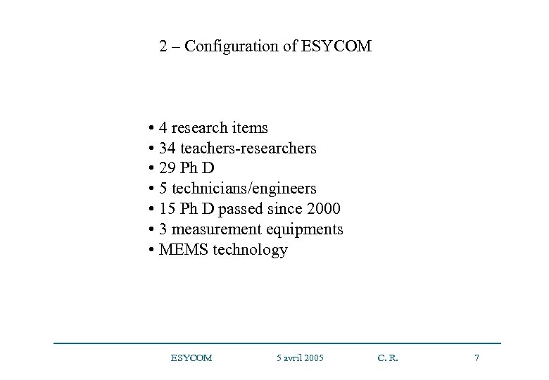 2 – Configuration of ESYCOM • 4 research items • 34 teachers-researchers • 29 Ph D • 5 technicians/engineers • 15 Ph D passed since 2000 • 3 measurement equipments • MEMS technology ESYCOM 5 avril 2005 C. R. 7
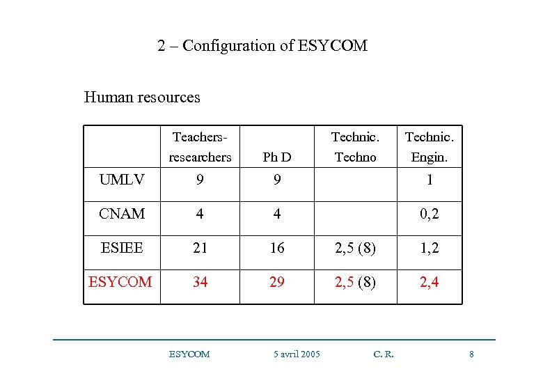 2 – Configuration of ESYCOM Human resources Teachersresearchers Ph D UMLV 9 9 1 CNAM 4 4 0, 2 ESIEE 21 16 2, 5 (8) 1, 2 ESYCOM 34 29 2, 5 (8) 2, 4 ESYCOM 5 avril 2005 Technic. Techno C. R. Technic. Engin. 8
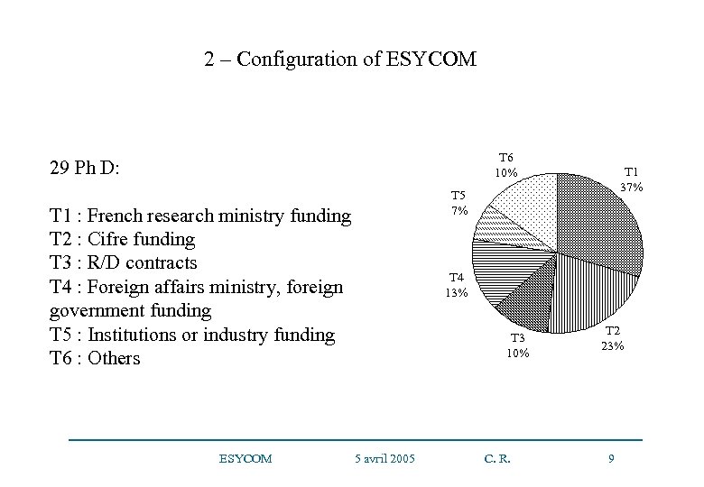 2 – Configuration of ESYCOM T 6 10% 29 Ph D: T 1 : French research ministry funding T 2 : Cifre funding T 3 : R/D contracts T 4 : Foreign affairs ministry, foreign government funding T 5 : Institutions or industry funding T 6 : Others ESYCOM 5 avril 2005 T 1 37% T 5 7% T 4 13% T 2 23% T 3 10% C. R. 9
 2 – Configuration of ESYCOM Main activities • European network of excellence: Network of Excellence in broadband Fiber Radio Techniques and its Integration Technologies: NEFERTITI • European network of excellence: Antenna Center of Excellence: ACE • 3 french RNRT (National Research Network in Telecommunications) contracts • 3 ANVAR contracts • 1 CNES contract • 1 CNRS contract • 1 ACI –Ville contract • etc… ESYCOM 5 avril 2005 C. R. 10
 2 – Configuration of ESYCOM Main activities • Organisation of Europan Microwave Week in Oct. 2000 in Paris La Défense: 3 conferences, 11 workshops, 3 short courses, 1 exhibition 2000 registrations conf. and workshops, 1300 visitors of exhibition, 38 countries • Organisation of 3 Summer Schools on “RF and Microwave Systems” - Sept. 2001: Architectures for RF systems (ESIEE) - Sept. 2002: Mastering of hertzian channel with several communication systems (UMLV) - March 2004: Advanced design of MMICs for millimeter waves, photonic and multifunction applications (CNAM) ESYCOM 5 avril 2005 C. R. 11
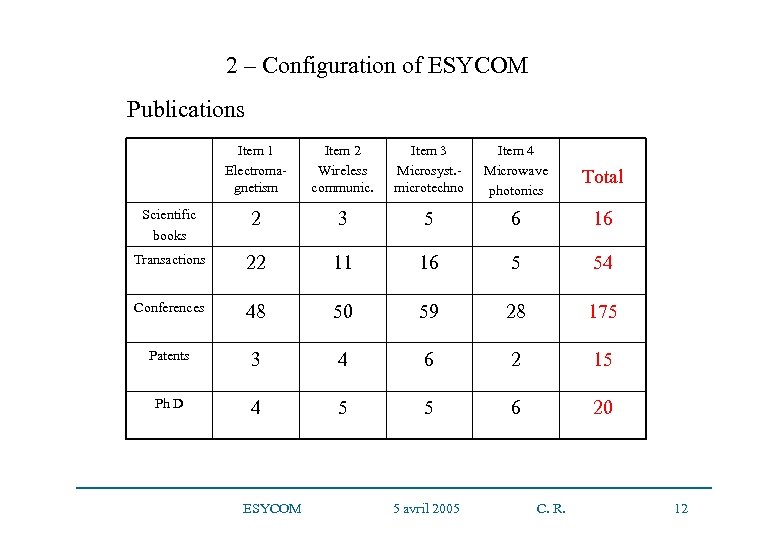 2 – Configuration of ESYCOM Publications Item 1 Electromagnetism Item 2 Wireless communic. Item 3 Microsyst. microtechno Item 4 Microwave photonics Total Scientific books 2 3 5 6 16 Transactions 22 11 16 5 54 Conferences 48 50 59 28 175 Patents 3 4 6 2 15 Ph D 4 5 5 6 20 ESYCOM 5 avril 2005 C. R. 12
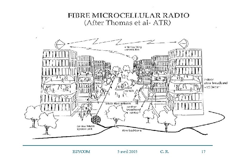
 3 – An example of item: microwave photonics • 3 professors, 2 lecturers, 4 passed Ph D, 5 Engineer diploma memoires Why microwave photonic links? • Signal distribution in phased array antennas : commercial satellites or military planes. A few metres. • Radio over fiber. Few km for microwaves over optics and a few tens of meters for hertzian microwave link • Optical distribution of a signal in very high bit rate electronic systems. A few m or a few tens of m. ESYCOM 5 avril 2005 C. R. 13
 ESYCOM 5 avril 2005 C. R. 14
 ESYCOM 5 avril 2005 C. R. 15
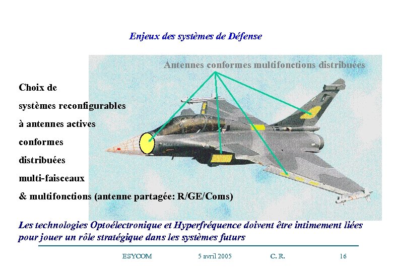 Enjeux des systèmes de Défense Antennes conformes multifonctions distribuées Choix de systèmes reconfigurables à antennes actives conformes distribuées multi-faisceaux & multifonctions (antenne partagée: R/GE/Coms) Les technologies Optoélectronique et Hyperfréquence doivent être intimement liées pour jouer un rôle stratégique dans les systèmes futurs ESYCOM 5 avril 2005 C. R. 16
 ESYCOM 5 avril 2005 C. R. 17
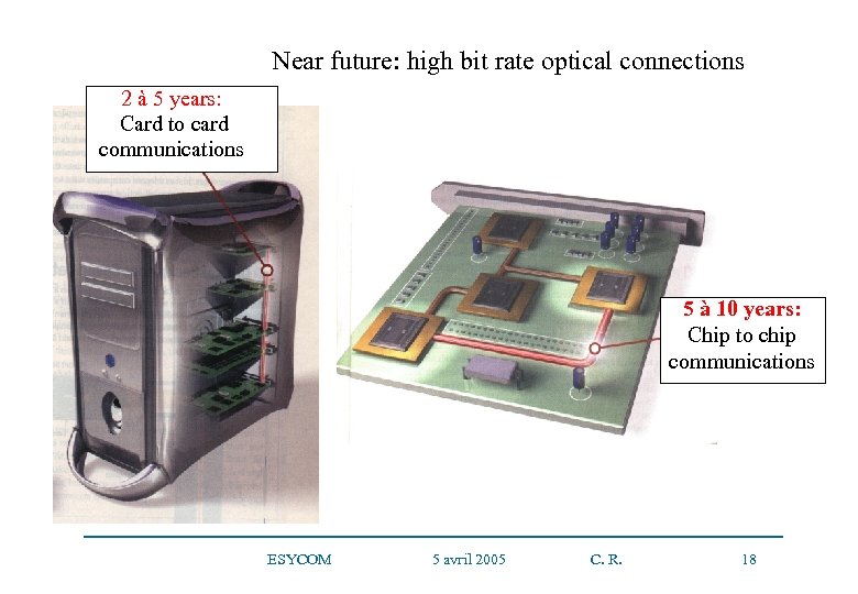 Near future: high bit rate optical connections 2 à 5 years: Card to card communications 5 à 10 years: Chip to chip communications ESYCOM 5 avril 2005 C. R. 18
 3 – An example of item: microwave photonics Circuits for microwave photonic links • Establishment of a library of models to simulate a complete microwave photonic link with a non linear frequency domain simulator ( ADS). Many simulations in gain, noise and non linearities of microwave photonic links (3 CNAM memoires + part of a thesis) ESYCOM + Thales Airborne Systems ESYCOM 5 avril 2005 C. R. 19
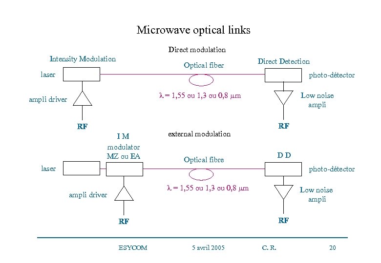 Microwave optical links Direct modulation Intensity Modulation Optical fiber Direct Detection laser photo-détector = 1, 55 ou 1, 3 ou 0, 8 µm ampli driver RF I M modulator MZ ou EA Low noise ampli RF external modulation Optical fibre D D laser photo-détector = 1, 55 ou 1, 3 ou 0, 8 µm ampli driver Low noise ampli RF RF ESYCOM 5 avril 2005 C. R. 20
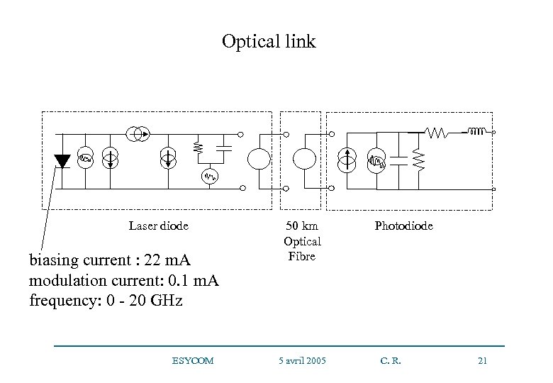 Optical link Laser diode biasing current : 22 m. A modulation current: 0. 1 m. A frequency: 0 - 20 GHz 50 km Optical Fibre ESYCOM 5 avril 2005 Photodiode C. R. 21
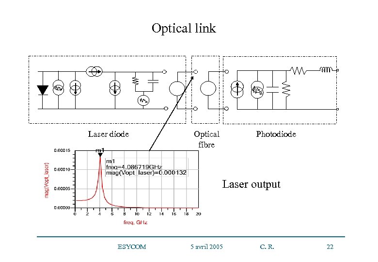 Optical link Laser diode Optical fibre Photodiode Laser output ESYCOM 5 avril 2005 C. R. 22
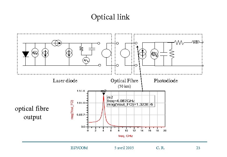 Optical link Laser diode Optical Fibre Photodiode (50 km) optical fibre output ESYCOM 5 avril 2005 C. R. 23
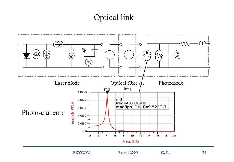 Optical link Laser diode Optical fibre (50 Photodiode km) Photo-current: ESYCOM 5 avril 2005 C. R. 24
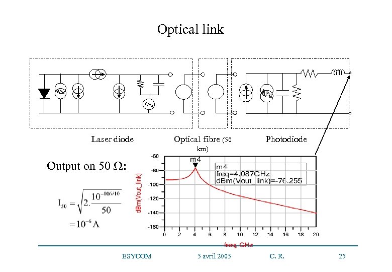 Optical link Laser diode Optical fibre (50 Photodiode km) Output on 50 : ESYCOM 5 avril 2005 C. R. 25
 3 – An example of item: microwave photonics Circuits for microwave photonic links • Opto amplifier at 30 GHz with In. P/Ga. In. As heterojunction phototransistors (HPT) (Ph D) Design: ESYCOM with our HPT models Technology: OPTO+ Marcoussis Measurements: LEST Brest ESYCOM 5 avril 2005 C. R. 26
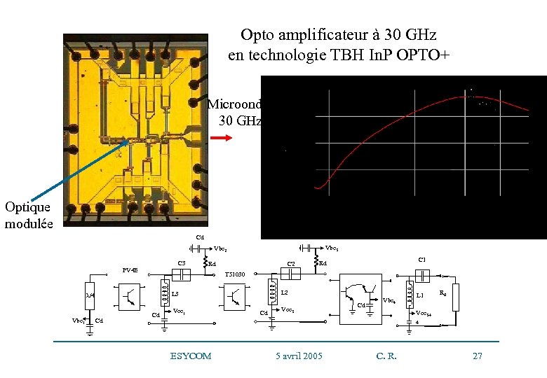 Opto amplificateur à 30 GHz en technologie TBH In. P OPTO+ Microondes 30 GHz Optique modulée Cd Cd Vbe 3 Vbe 2 C 3 PV 4 E L 2 L 3 Cd C 1 Rd T 51030 /4 Vbe 1 C 2 Rd Cd Vce 1 Cd Vce 3 Cd Vbe 4 L 1 R 0 Vce 3+ 4 ESYCOM 5 avril 2005 C. R. 27
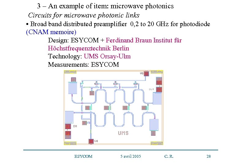 3 – An example of item: microwave photonics Circuits for microwave photonic links • Broad band distributed preamplifier 0, 2 to 20 GHz for photodiode (CNAM memoire) Design: ESYCOM + Ferdinand Braun Institut für Höchstfrequenztechnik Berlin Technology: UMS Orsay-Ulm Measurements: ESYCOM 5 avril 2005 C. R. 28
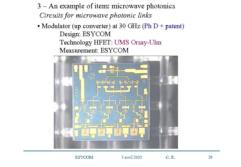 3 – An example of item: microwave photonics Circuits for microwave photonic links • Modulator (up converter) at 30 GHz (Ph D + patent) Design: ESYCOM Technology HFET: UMS Orsay-Ulm Measurement: ESYCOM 5 avril 2005 C. R. 29
 3 – An example of item: microwave photonics Circuits for microwave photonic links • Frequency tripler 12, 66 -38 GHz (Ph D) Design: ESYCOM HFET technology : OMMIC Limeil Brévanne Measurements: ESYCOM + Agilent Palo Alto • Chipset for transmitter and receiver of UWB signals (3, 6 -10, 7 GHz) (Ph D) Design: ESYCOM Technology: UMS Orsay-Ulm Measurements: ESYCOM + ENSTA Paris ESYCOM 5 avril 2005 C. R. 30
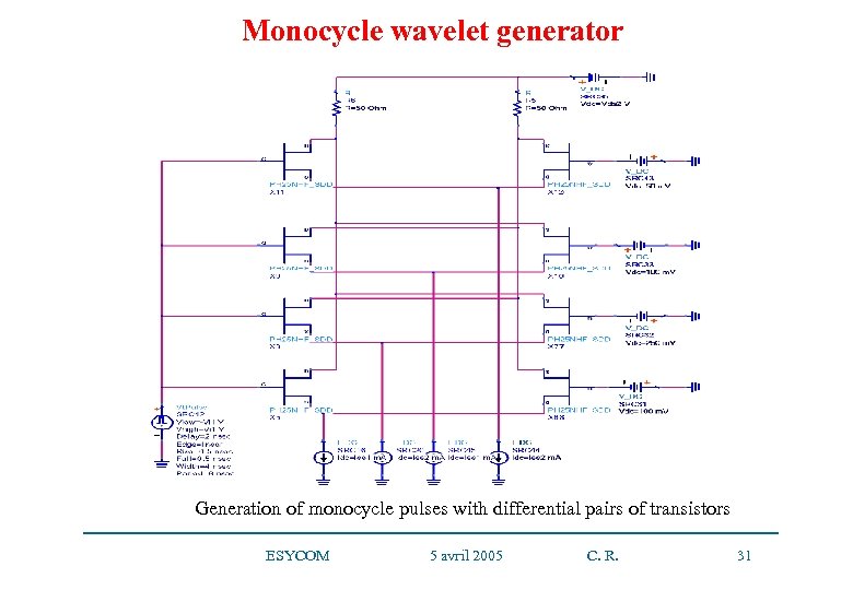 Monocycle wavelet generator Generation of monocycle pulses with differential pairs of transistors ESYCOM 5 avril 2005 C. R. 31
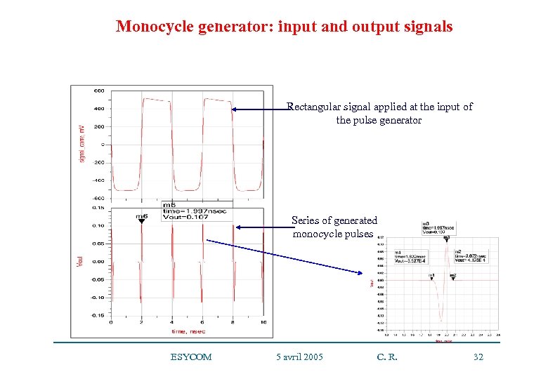 Monocycle generator: input and output signals Rectangular signal applied at the input of the pulse generator Series of generated monocycle pulses ESYCOM 5 avril 2005 C. R. 32
 3 – An example of item: microwave photonics Microwave photonic components • In. P/Ga. In. As heterojunction phototransistor (HPT) (Ph D) Numerical and physical simulations of semiconductor devices in finite differences : ESYCOM Measuremens: OPTO+ Marcoussis, LEST Brest, ESYCOM • New concepts (optoelectronic S parameters) for optoelectronic modelling of a HPT: ESYCOM 5 avril 2005 C. R. 33
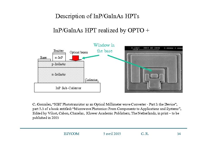 Description of In. P/Ga. In. As HPTs In. P/Ga. In. As HPT realized by OPTO + Emitter Base Optical beam Window in the base n-In. P p-In. Ga. As n-In. Ga. As Collector In. P Sub -Collector C. Gonzalez, “HBT Phototransistor as an Optical Millimeter wave Converter - Part I: the Device”, part 5. 3 of a book entitled: “Microwave Photonics: From Components to Applications and Systems”, Edited by Vilcot, Cabon, Chazelas, Kluwer Academic Publishers, The Netherlands, in print – to be published in 2003 ESYCOM 5 avril 2005 C. R. 34
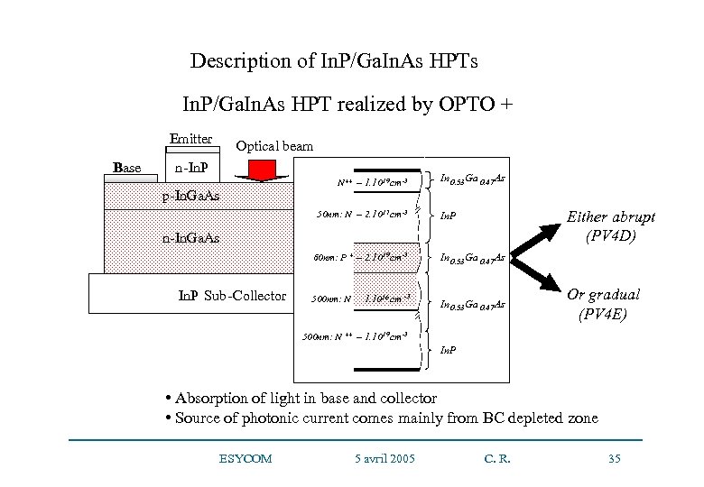 Description of In. P/Ga. In. As HPTs In. P/Ga. In. As HPT realized by OPTO + Emitter Base Optical beam n-In. P p-In. Ga. As N ++ – 1. 10 19 cm -3 50 nm: N – 2. 10 17 cm -3 In 0. 53 Ga 0. 47 As Either abrupt (PV 4 D) In. P n-In. Ga. As 60 nm: P Collector – 2. 10 + In. P Sub -Collector 19 cm -3 16 - -3 500 nm: N – 1. 1016 cm -3 In 0. 53 Ga 0. 47 As Or gradual (PV 4 E) In 0. 53 Ga 0. 47 As 500 nm: N ++ – 1. 10 19 cm -3 In. P • Absorption of light in base and collector • Source of photonic current comes mainly from BC depleted zone ESYCOM 5 avril 2005 C. R. 35
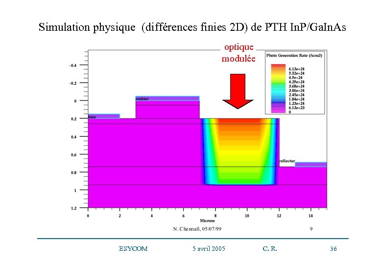 Simulation physique (différences finies 2 D) de PTH In. P/Ga. In. As optique modulée ESYCOM 5 avril 2005 C. R. 36
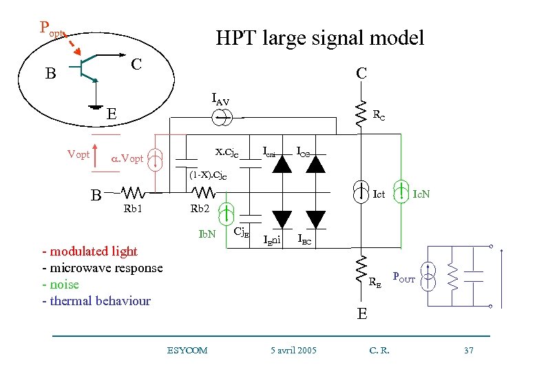 Popt HPT large signal model C B C IAV E Vopt RC X. Cj. C . Vopt Icni ICC (1 -X). Cj. C B Ict Rb 1 Rb 2 Ib. N - modulated light - microwave response - noise - thermal behaviour Ic. N Cj. E IEni IEC ESYCOM 5 avril 2005 RE POUT E C. R. 37
 3 – An example of item: microwave photonics Microwave photonic components • Si/Si. Ge phototransistor (Ph D) Physical simulation and design: ESYCOM Technology: Atmel Heilbronn through Université of Ulm Microwave measurements : IEF Orsay Optoelectronic measurements: ESYCOM • First world result for a Si/Si. Ge HPT • Comparison with other teams in the world (Germany, France, Israel, Taïwan, USA) in a workshop organised by ESYCOM in Budapest in Sept. 2003 in association with an IEEE Topical Meeting on Microwave Photonics • For a Si/Si. Ge HPT, a team of the University of Taïwan began with a MQW structure and recently switched to our solution. ESYCOM 5 avril 2005 C. R. 38
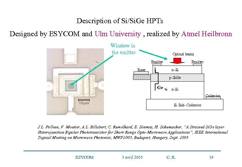 Description of Si/Si. Ge HPTs Designed by ESYCOM and Ulm University , realized by Atmel Heilbronn Window in the emitter Optical beam Emitter Base Emitter n-Si p-Si. Ge Ge % n-Si Collector Si Sub-Collector J. L. Polleux, F. Moutier, A. L. Billabert, C. Rumelhard, E. Sönmez, H. Schumacher, “A Strained Si. Ge layer Heterojunction Bipolar Phototransistor for Short-Range Opto-Microwave Applications”, IEEE International Topical Meeting on Microwave Photonics, MWP 2003, Budapest, Hungary, Sept. 2003 ESYCOM 5 avril 2005 C. R. 39
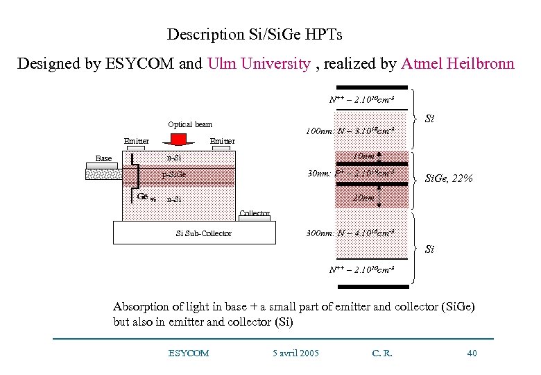 Description Si/Si. Ge HPTs Designed by ESYCOM and Ulm University , realized by Atmel Heilbronn N++ – 2. 1020 cm-3 Si Optical beam Emitter 100 nm: N – Emitter 10 nm n-Si Base 30 nm: P+ – 2. 1019 cm-3 p-Si. Ge Ge % 3. 1018 cm-3 Si. Ge, 22% 20 nm n-Si Collector Si Sub-Collector 300 nm: N – 4. 1016 cm-3 Si N++ – 2. 1020 cm-3 Absorption of light in base + a small part of emitter and collector (Si. Ge) but also in emitter and collector (Si) ESYCOM 5 avril 2005 C. R. 40
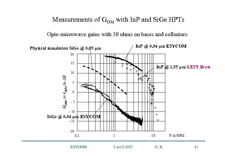 Measurements of GOM with In. P and Si. Ge HPTs Opto-microwave gains with 50 ohms on bases and collectors In. P @ 0. 94 µm ESYCOM Physical simulation Si. Ge @ 0. 85 µm 20 20 15 15 In. P @ 1. 55 µm LEST Brest 10 GOM or r. HPT in d. B 10 5 0 - 5 -5 - 10 -10 Si. Ge @ 0. 94 µm ESYCOM - 15 -20 - 20 10 8 0. 1 10 9 1 ESYCOM 5 avril 2005 10 10 10 C. R. F in GHz 41
 3 – An example of item: microwave photonics Microwave photonic components • Improving the frequency response of Si/Si. Ge PTH by a focalisation of optical absorption in the base by optimisation of optical wavelength (Ph D) Physical simulations : ESYCOM Future technology : Atmel Heilbronn through University of Ulm ESYCOM 5 avril 2005 C. R. 42
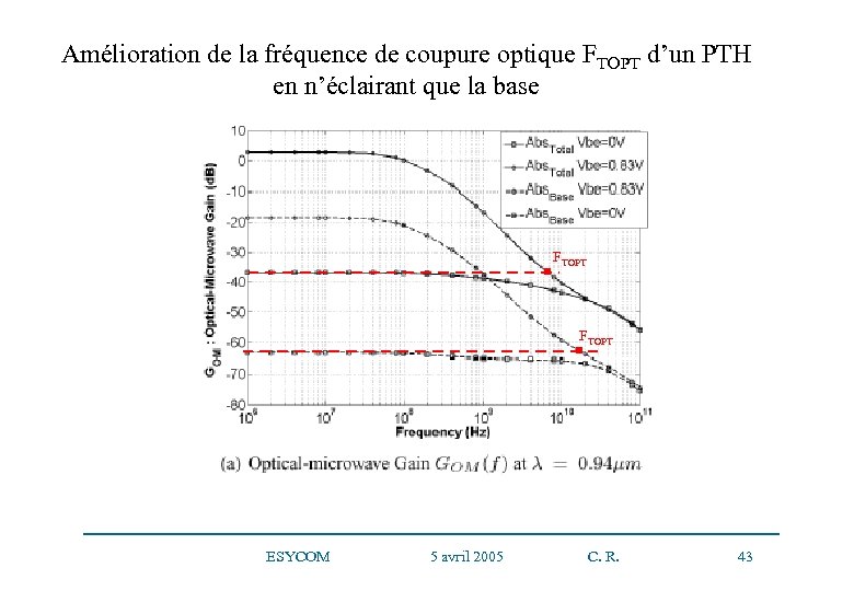 Amélioration de la fréquence de coupure optique FTOPT d’un PTH en n’éclairant que la base FTOPT ESYCOM 5 avril 2005 C. R. 43
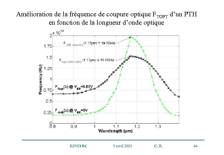 Amélioration de la fréquence de coupure optique FTOPT d’un PTH en fonction de la longueur d’onde optique ESYCOM 5 avril 2005 C. R. 44
 3 – An example of item: microwave photonics Microwave photonic components • Improving the responsivity of a Si/Si. Ge by insertion in a horizontal optical cavity constituted of adjustable Bragg reflectors (Ph D) Optimisation of the number of blades of the Bragg reflector to improve absorption: ESYCOM MEMS Si technology for Bragg reflectors: ESYCOM 5 avril 2005 C. R. 45
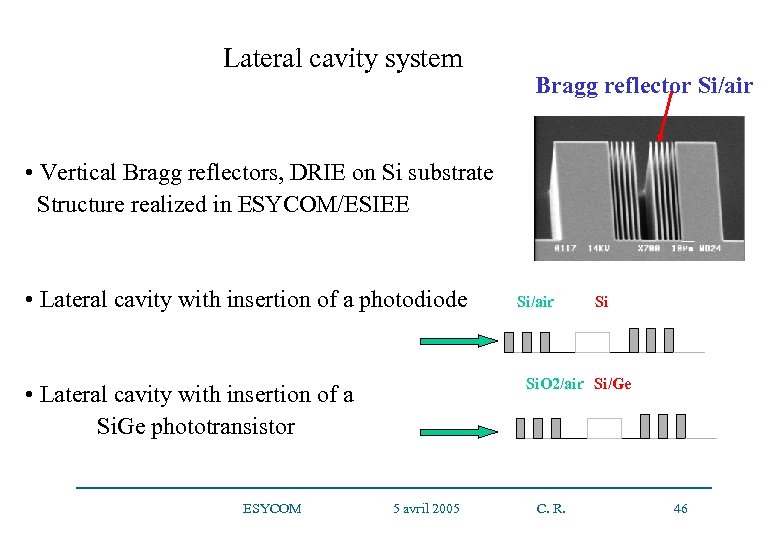 Lateral cavity system Bragg reflector Si/air • Vertical Bragg reflectors, DRIE on Si substrate Structure realized in ESYCOM/ESIEE • Lateral cavity with insertion of a photodiode • Lateral cavity with insertion of a Si. Ge phototransistor ESYCOM 5 avril 2005 Si/air Si Si. O 2/air Si/Ge C. R. 46
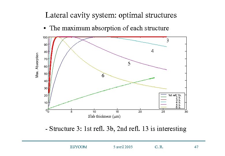 Lateral cavity system: optimal structures • The maximum absorption of each structure 100 3 Max. Absorption 90 4 80 70 5 60 50 6 40 30 Si slab thickness (µm) 1 st refl 1 b. 2 b. 3 b. 4 b. 5 b. 6 b. 20 10 0 0 5 10 15 20 25 30 Slab thickness (µm) - Structure 3: 1 st refl. 3 b, 2 nd refl. 13 is interesting ESYCOM 5 avril 2005 C. R. 47
 3 – An example of item: microwave photonics Microwave photonic components • Study of a phase shifter constituted of two coupled optical cavities realized with Bragg reflectors (Ph D) Design of adjustable micro-photonic circuit: ESYCOM + IEF Orsay Future realization with a MEMS technology on Si: ESYCOM 5 avril 2005 C. R. 48
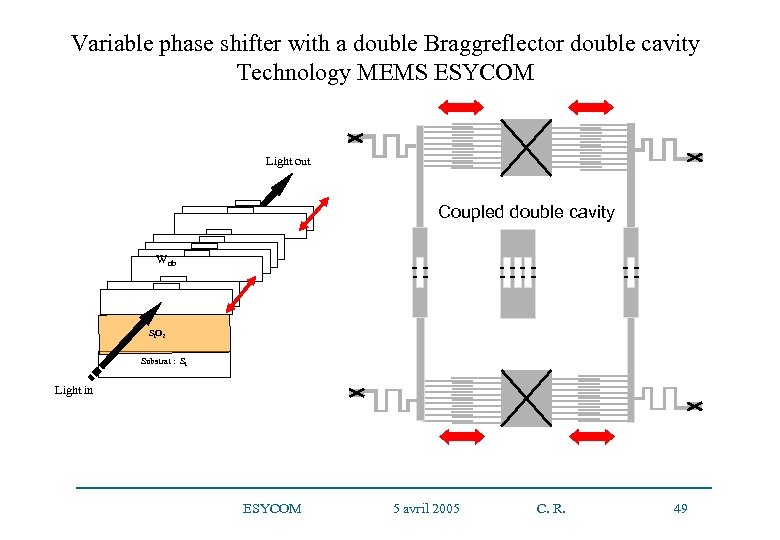 Variable phase shifter with a double Braggreflector double cavity Technology MEMS ESYCOM Light out Coupled double cavity Wrib Si. O 2 Substrat : Si Light in ESYCOM 5 avril 2005 C. R. 49
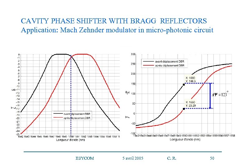 CAVITY PHASE SHIFTER WITH BRAGG REFLECTORS Application: Mach Zehnder modulator in micro-photonic circuit ESYCOM 5 avril 2005 C. R. 50
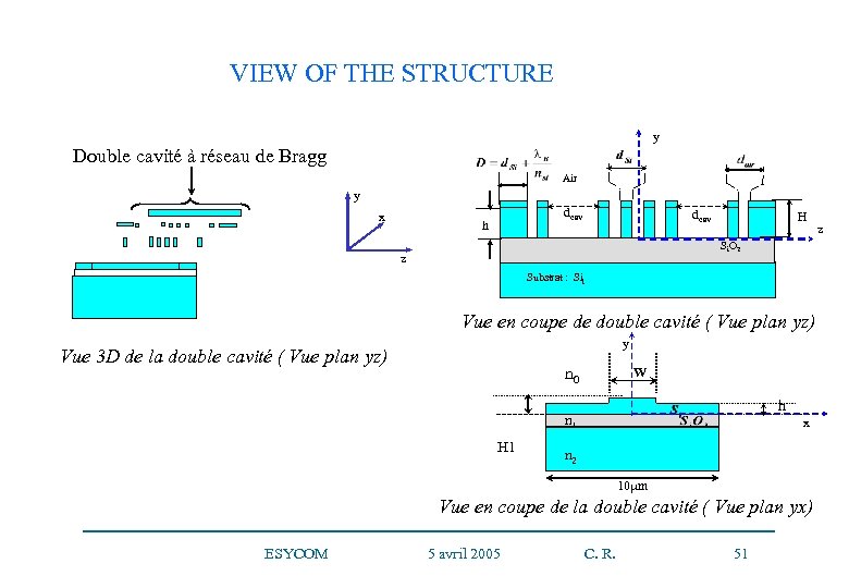 VIEW OF THE STRUCTURE y Double cavité à réseau de Bragg Air y x dcav h dcav H Si. O 2 z Substrat : Sii Vue en coupe de double cavité ( Vue plan yz) y Vue 3 D de la double cavité ( Vue plan yz) n 0 W h x n 1 H 1 x n 2 10 mm Vue en coupe de la double cavité ( Vue plan yx) ESYCOM 5 avril 2005 C. R. 51 z
 4 – Synthesis and prospects Microwave photonic item: • First realization of a Si/Si. Ge microwave HPT • Necessity to have an access to different technologies: Atmel Ulm, OPTO+ Marcoussis, OMMIC Limeil Brévanne, UMS Orsay-Ulm • Direct acces to ESIEE MEMS Si technology for micro-photonic circuits • Measurements realized in Brest, Orsay, Marne la Vallée and Paris ESYCOM: • Many contacts with other items of ESYCOM • Also contacts with other microwave photonics teams in Paris (Paris VI) ESYCOM 5 avril 2005 C. R. 52


