f688ad1284122460b013f96fd4a1704e.ppt
- Количество слайдов: 45
Encrypted Transaction with Triple DES Objective: To implement a secure credit card transaction using 3 DES encryption using Kerberos-style authentication. Team W 2 Yervant Dermenjian Taewan Kim Evan Mengstab Xiaochun Zhu (W 21) (W 22) (W 23) (W 24) Design Manager: Rebecca Miller Final Presentation April 28, 2004
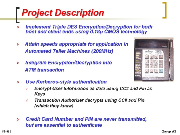
Project Description Ø Implement Triple DES Encryption/Decryption for both host and client ends using 0. 18μ CMOS technology Ø Attain speeds appropriate for application in Automated Teller Machines (200 MHz) Ø Integrate Encryption/Decryption into ATM transaction Ø Use Kerberos-style authentication ü ü Ø 18 -525 Encrypt User Information as data using CC# and Pin as Keys Transaction Authorizer decrypts using CC# and Pin (which they know) Credit Card Number and PIN are never transmitted, but are essential to authenticate Group W 2

Security In Making Purchases Ø Ø Identity theft is a growing problem Ø 18 -525 Point-of-sale terminals transmit your name, credit card number, and expiration dates ‘in the clear’ Credit and charge card fraud costs cardholders and issuers hundreds of millions of dollars each year Group W 2
Triple Data Encryption Standard Ø Difficult to decipher for large encryption keys Ø Symmetric Key Cipher – encryption & decryption use same key Ø Based on DES – a very trusted cipher Ø Master. Card requires all ATMs be 3 DES compliant by April 1, 2005 Ø Ø 18 -525 Accepted as the new standard for federal agencies in 1999 Finalist for the 2001 Advanced Encryption Standard Group W 2
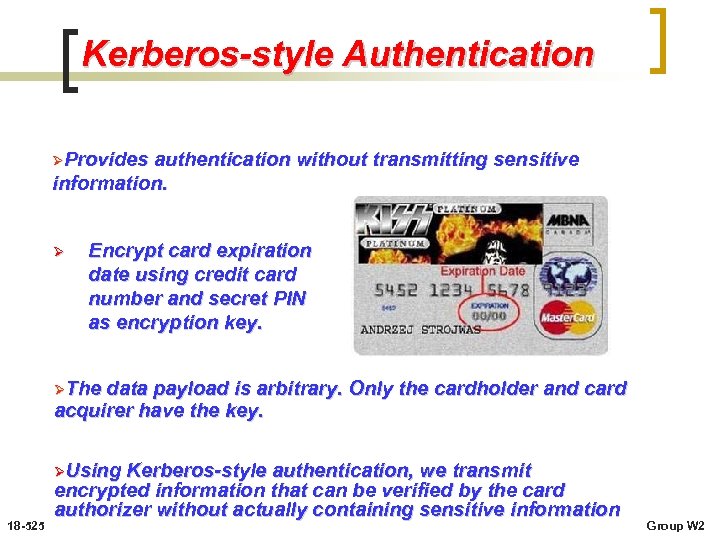
Kerberos-style Authentication ØProvides authentication without transmitting sensitive information. Ø Encrypt card expiration date using credit card number and secret PIN as encryption key. ØThe data payload is arbitrary. Only the cardholder and card acquirer have the key. ØUsing 18 -525 Kerberos-style authentication, we transmit encrypted information that can be verified by the card authorizer without actually containing sensitive information Group W 2
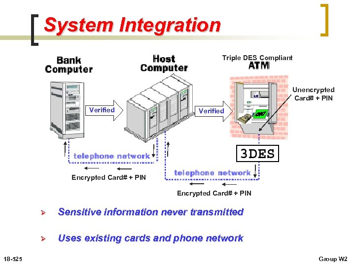
System Integration Triple DES Compliant Unencrypted Card# + PIN Verified Encrypted Card# + PIN Ø Ø 18 -525 Sensitive information never transmitted Uses existing cards and phone network Group W 2
How It Works Ø Ø Card company has CC# and PIN to decrypt packet Ø If expiration date matches, purchase is approved Ø 18 -525 Transmit: name, merchant, price, encrypted expiration date CC# and PIN are never transmitted, but essential to authenticate Group W 2
The 3 DES Algorithm Ø Overview ü ü Ø DES vs. 3 DES ü ü Ø 3 DES applies 3 stages of DES with a separate key for each stage Total key length in 3 DES is 56 bits x 3 keys = 168 bits Stages ü ü ü 18 -525 Block Cipher - acts on a 64 -bit block of plaintext Converts it into a 64 -bit block of cipher text using a 56 -bit key Specified in FIPS Pub 46 -3 Symmetric Key Cipher – encryption & decryption use same key Stage 1: Encrypt plaintext with Key 1 Stage 2: Decrypt cipher text from Stage 1 with Key 2 (produces new cipher text) Stage 2: Encrypt cipher text from Stage 2 with Key 3 Group W 2
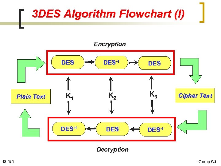
3 DES Algorithm Flowchart (I) Encryption DES K 1 K 2 K 3 DES-1 Plain Text DES-1 DES Cipher Text DES-1 Decryption 18 -525 Group W 2
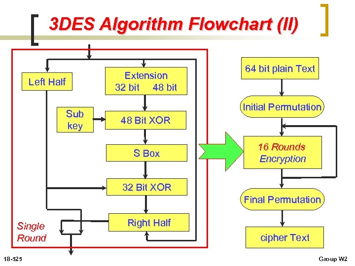
3 DES Algorithm Flowchart (II) Extension 32 bit 48 bit Left Half Sub key 64 bit plain Text Initial Permutation 48 Bit XOR S Box 16 Rounds Encryption 32 Bit XOR Final Permutation Single Round 18 -525 Right Half cipher Text Group W 2
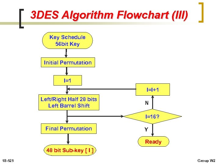
3 DES Algorithm Flowchart (III) Key Schedule 56 bit Key Initial Permutation I=1 I=I+1 Left/Right Half 28 bits Left Barrel Shift N I=16? Final Permutation Y Ready 48 bit Sub-key [ I ] 18 -525 Group W 2
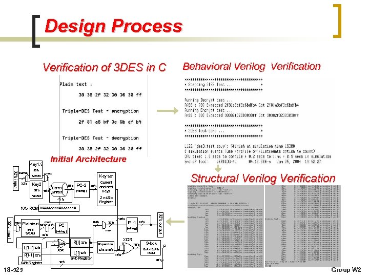
Design Process Verification of 3 DES in C Initial Architecture Key 1, 3 32’b input demux 32’b 56’b mux SRAM Key 2 56’b Barrel Shifter PC-2 56’b Current 48’b and next keys (wiring) 2 x 48’b Register 1’b Plaintext I: 0, 0, 1, 1, 1, 0 mux 64’b 32’b 64’b SRAM 48’b 32’b mux (wiring) IP -1 32’b (wiring) 32’b L[I-1] 32’b XOR R[I-1] 32’b 64’b Register 18 -525 64’b PC 32’b output 32’b input mux Structural Verilog Verification Key set SRAM 16’b ROM Behavioral Verilog Verification R[I] 32’b L[I] 32’b 64’b Register 32’b XOR Expansion 32’b 48’b S-box 8 x 4 x 16 x 4’b ROM P 48’b Group W 2
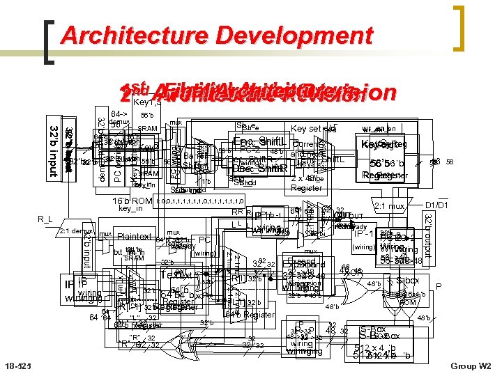
Architecture Development Initial Architecture Final Architecture 1 st Architecture Revision 2 nd Architecture Revision Key 1, 3 mux 56’b SRAM Text 2: 1 mux 32’b 64 64 64’b ’b’b XOR Register R[I-1] 32’b Register 32 “L” “L 32 32 ” 64’b Register “R ” 32 “R” “R ” 32 32 18 -525 2 x 48’b Sh_e Register 56 56 56 ’b 56’b ’b Register D 1/D 1 2: 1 mux 32 32 32 OUT OUT ready 48’b ready wiring 64’b 32’b-2 32’b IP -1 PC-2 -2 PC PC Wiring (wiring) Wiring mux 56 ->48 32 56 ->48 Expand 56 ->48 32 32 Expand 48 48 48 32 ->48 XOR 32 ->48 32 ->48 R[I] 32’b S-box Expansion wiring 48’b P wiring 64 R R R IP -1 -1 64 64 IP-1 IP L L L wiring 2: 1 mux 64’b 32’b PC ready (wiring) 32’b L[I-1] 32’b “L” Sh_d 2: 1 mux 64 64 Key. Reg Key. Sub Key. Reg 32’b output SRAM Current PC-2 48’b and next Enc_Shift. L Dec_Shift. R (wiring) keys Dec_Shift. R 56’b 2: 1 mux 32’b input txt_in 64’b txt_in IP IP IP wiring 64 Plaintext Enc_Shift. L wr_en I: 0, 0, 1, 1, 1, 0 R_L 2: 1 demux Key set e/d 2: 1 mux key_in Barrel Shifter 1’b Sub_rnd key_in 16’b ROM 2: 1 mux PC (wiring) Key Latch PC (wiring) demux 32 ’b Latch 32’b 32 ’b Latch 56’b 32 ’b Sh_e 2: 1 mux 56’b SRAM 64’b 56’b 32 ’b Latch 32’b 2: 132 ’b Latch Key 2 32 ’b input 32’b input 64 -> demux 56 L[I] 32’b 48’b 64’b Register 32’b P 32 32 32 8 x 4 x 16 x 4’b ROM 48’b 32 ->32 P P 48 ->32 32 wiring 32 48’b S-Box S-Box 512 x 4 ’b 512 x 4’b ’b Group W 2
Floorplan Evolution 18 -525 Group W 2
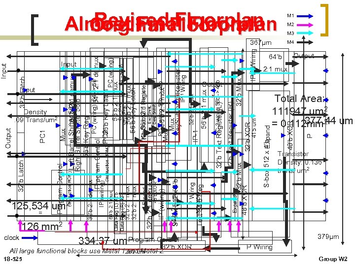
125, 534 um 2 = clock 18 -525 PC 1 Input Density. 09 Trans/um 2 32’b Latch Input . 126 mm 2 All large functional blocks use Metal 1269 um and Metal 2. 334. 37 um Program Control. XOR 32’b 64 -> 56 56’b 2: 1 mux 32’b 2: 1 mux PC-2 wiring 56 b 32’b Text Register (L) -> 48 b IP-1 IP Wiring Mux 56’b 2: 1 mux Mux Key. Sub 56’b-1 Register PC-2 wiring 56 b -> 48 b Enc_Shift. L Des_Shift. R Key. Sub 56’b Register IP 56’b 2: 1 mux 56’b Key Latch Enc_Shift. L Dec_Shift. L Output Expand S-box 512 x 4’b Expand 32’b Text Register (R) 32’b Mux 48’b XOR 32’b XOR IP-1 Wiring 415 um Text 32’b XOR 64’b Reg P Wiring 64’b 2: 1 mux S-box 512 x 4’b IP (wiring) 48’b XOR 32’b 2: 1 demux Expand 32’b 2: 1 mux Data Reg (R) 32’b (Instruction ROM) Mux Left Barrel Shifter 56’b demux 64’b 2: 1 Right Barrel Shifter 56’b Key Reg 32’b 2: 1 demux PC (wiring) 64’b 2: 1 demux 64 -> 56 Program Control IP (wiring) 56’b Key Latch (Instruction ROM) PC 2 64’b 2: 1 mux PC (wiring) 56’b 2: 1 mux Data Reg (L) 32’b Program Control 32’b Latch Output 64’b P 367μm Total Area: 111947 um 2 377. 44 = 0. 112 mm 2 um Transistor Density: 0. 136 trans/ um 2 48’b XOR Revised Floorplan Almost Final Floorplan Original Floorplan M 1 M 2 M 3 M 4 Output 2: 1 mux 379μm P Wiring Group W 2
Final Floorplan OUTPUT INPUT OUTPUT 18 -525 Group W 2
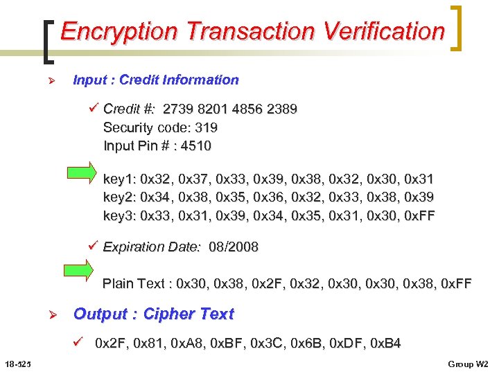
Encryption Transaction Verification Ø Input : Credit Information ü Credit #: 2739 8201 4856 2389 Security code: 319 Input Pin # : 4510 key 1: 0 x 32, 0 x 37, 0 x 33, 0 x 39, 0 x 38, 0 x 32, 0 x 30, 0 x 31 key 2: 0 x 34, 0 x 38, 0 x 35, 0 x 36, 0 x 32, 0 x 33, 0 x 38, 0 x 39 key 3: 0 x 33, 0 x 31, 0 x 39, 0 x 34, 0 x 35, 0 x 31, 0 x 30, 0 x. FF ü Expiration Date: 08/2008 Plain Text : 0 x 30, 0 x 38, 0 x 2 F, 0 x 32, 0 x 30, 0 x 38, 0 x. FF Ø Output : Cipher Text ü 0 x 2 F, 0 x 81, 0 x. A 8, 0 x. BF, 0 x 3 C, 0 x 6 B, 0 x. DF, 0 x. B 4 18 -525 Group W 2
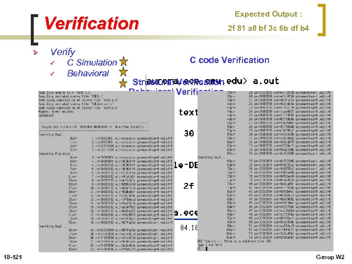
Expected Output : Verification Ø Verify ü ü ü 18 -525 C Simulation Behavioral Structural 2 f 81 a 8 bf 3 c 6 b df b 4 C code Verification Structural Verification Behavioral Verification Group W 2
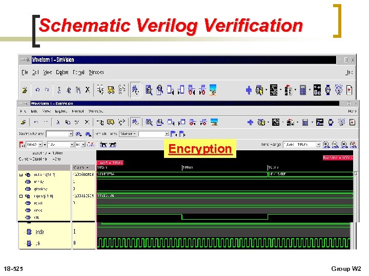
Schematic Verilog Verification Encryption 18 -525 Group W 2
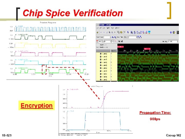
Chip Spice Verification Encryption Propagation Time: 908 ps 18 -525 Group W 2
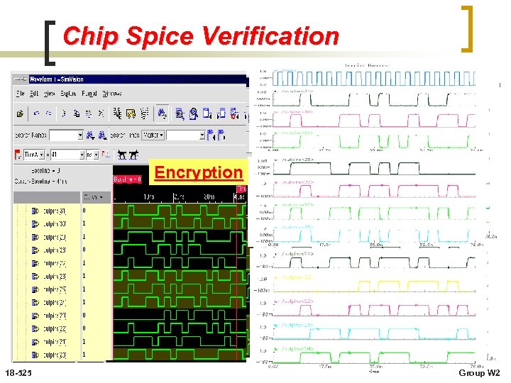
Chip Spice Verification Encryption 18 -525 Group W 2
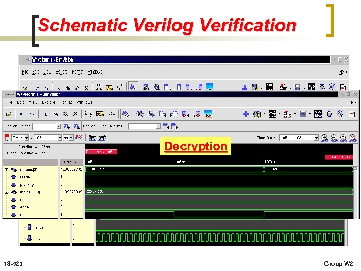
Schematic Verilog Verification Decryption 18 -525 Group W 2
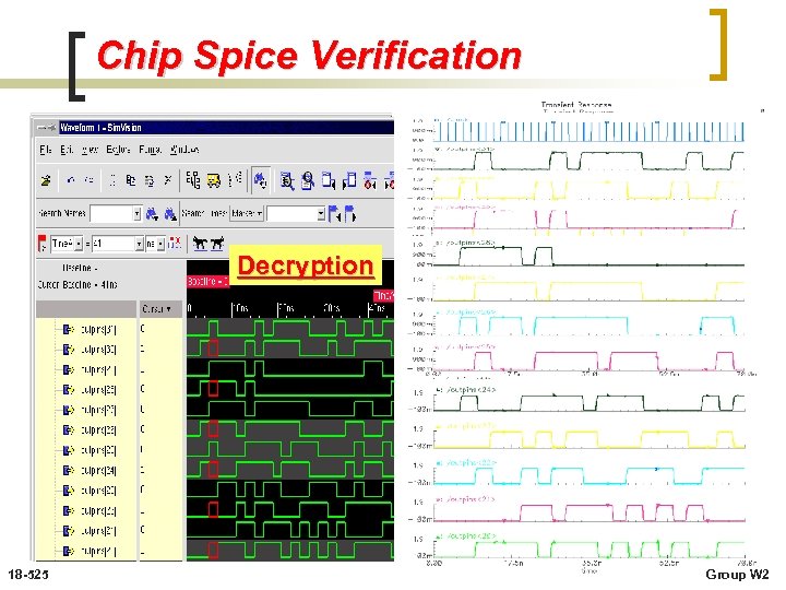
Chip Spice Verification Decryption 18 -525 Group W 2
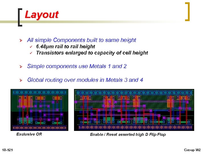
Layout Ø All simple Components built to same height ü ü 6. 48μm rail to rail height Transistors enlarged to capacity of cell height Ø Simple components use Metals 1 and 2 Ø Global routing over modules in Metals 3 and 4 Exclusive OR 18 -525 Enable / Reset asserted high D Flip Flop Group W 2
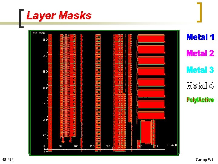
Layer Masks 18 -525 Group W 2
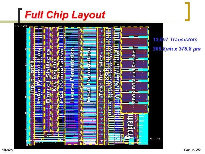
Full Chip Layout 13, 697 Transistors 366. 8μm x 378. 8 μm 18 -525 Group W 2
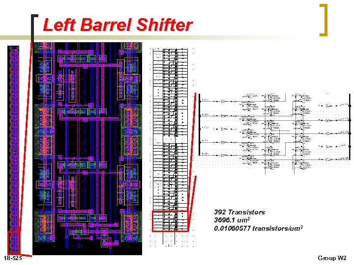
Left Barrel Shifter 392 Transistors 3696. 1 um 2 0. 01060577 transistors/um 2 18 -525 Group W 2
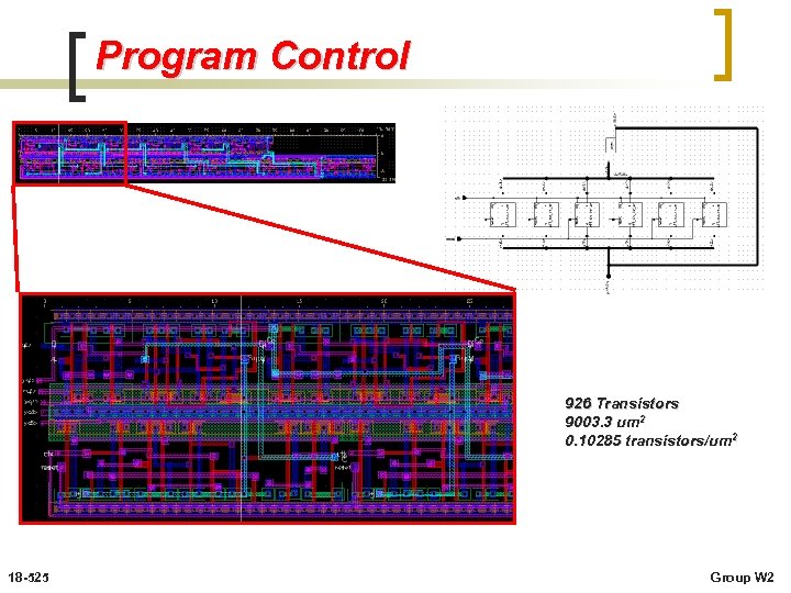
Program Control 926 Transistors 9003. 3 um 2 0. 10285 transistors/um 2 18 -525 Group W 2
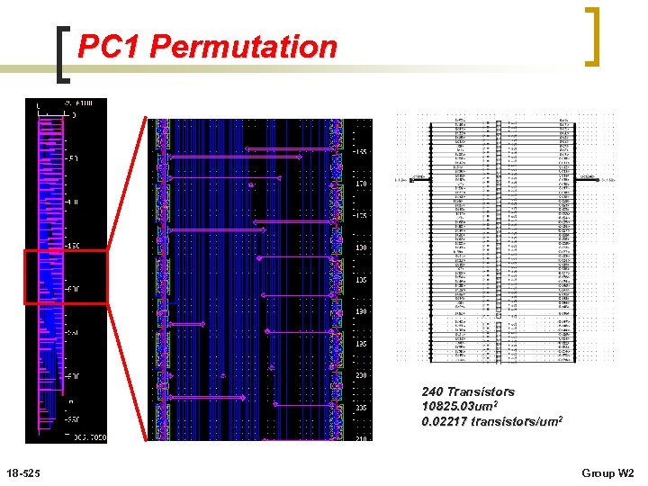
PC 1 Permutation 240 Transistors 10825. 03 um 2 0. 02217 transistors/um 2 18 -525 Group W 2
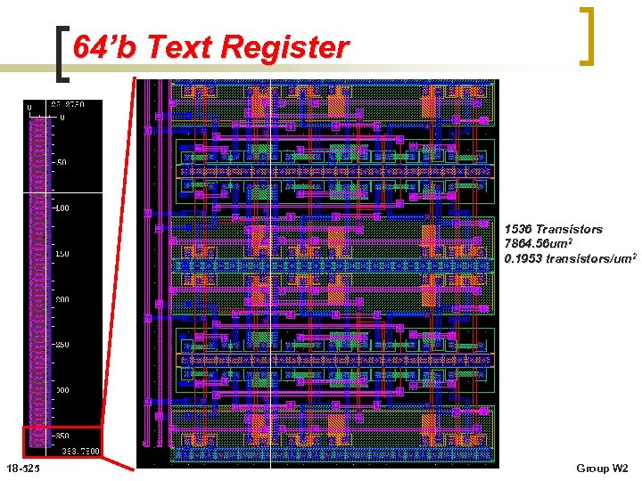
64’b Text Register 1536 Transistors 7864. 56 um 2 0. 1953 transistors/um 2 18 -525 Group W 2
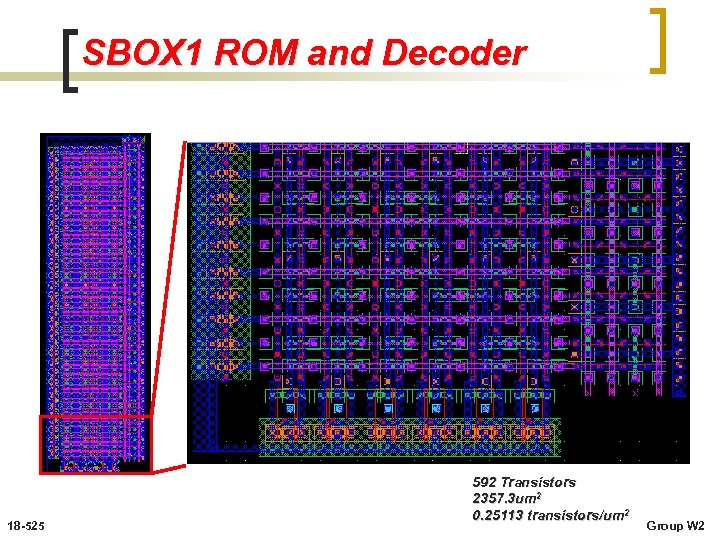
SBOX 1 ROM and Decoder 18 -525 592 Transistors 2357. 3 um 2 0. 25113 transistors/um 2 Group W 2
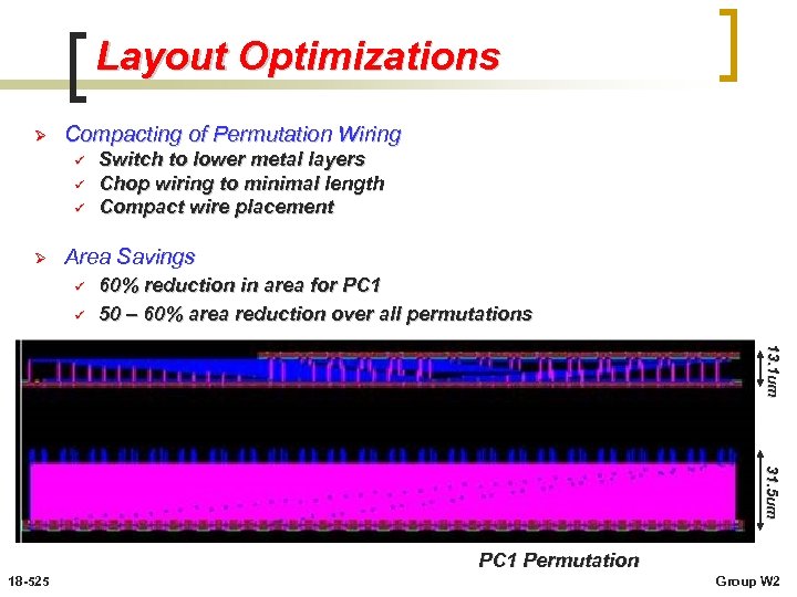
Layout Optimizations Ø Compacting of Permutation Wiring ü ü ü Ø Switch to lower metal layers Chop wiring to minimal length Compact wire placement Area Savings ü ü 60% reduction in area for PC 1 50 – 60% area reduction over all permutations 13. 1 um 31. 5 um PC 1 Permutation 18 -525 Group W 2
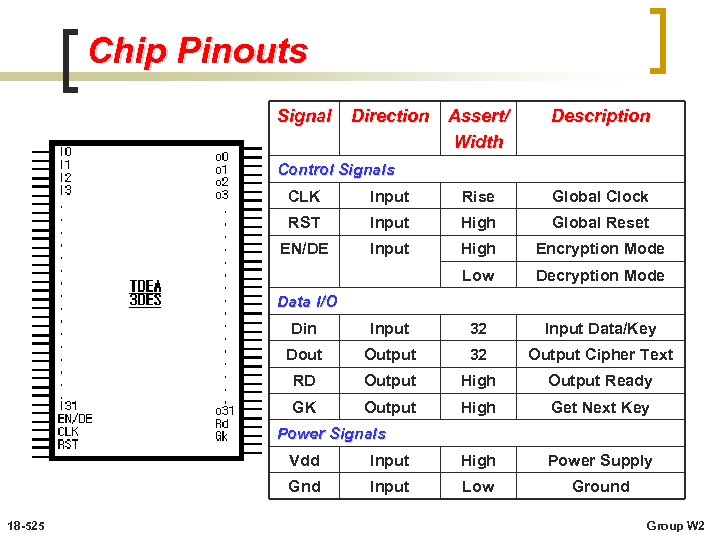
Chip Pinouts Signal Direction Assert/ Width Description Control Signals CLK Input Rise Global Clock RST Input High Global Reset EN/DE Input High Encryption Mode Low Decryption Mode Data I/O Din Input 32 Input Data/Key Dout Output 32 Output Cipher Text RD Output High Output Ready GK Output High Get Next Key Power Signals Vdd High Power Supply Gnd 18 -525 Input Low Ground Group W 2
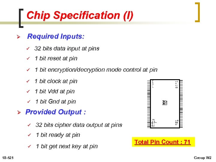
Chip Specification (I) Ø Required Inputs: ü ü 1 bit reset at pin ü 1 bit encryption/decryption mode control at pin ü 1 bit clock at pin ü 1 bit Vdd at pin ü Ø 32 bits data input at pins 1 bit Gnd at pin Provided Output : ü ü 1 bit ready at pin ü 18 -525 32 bits cipher data output at pins 1 bit get next key at pin Total Pin Count : 71 Group W 2
Chip Specifications (II) Ø Total Pin Count: 71 Ø Chip Size: 366. 8 μm x 378. 8 μm Ø Chip Area: 138943. 8 μm 2 Ø Chip Aspect Ratio: 1: 1. 03 Ø Transistor Count: 13, 697 (PMOS: 4, 324 NMOS: 9, 373) Ø Transistor Density: 0. 09847 transistors/μm 2 10. 155 μm 2/transistor 18 -525 Group W 2
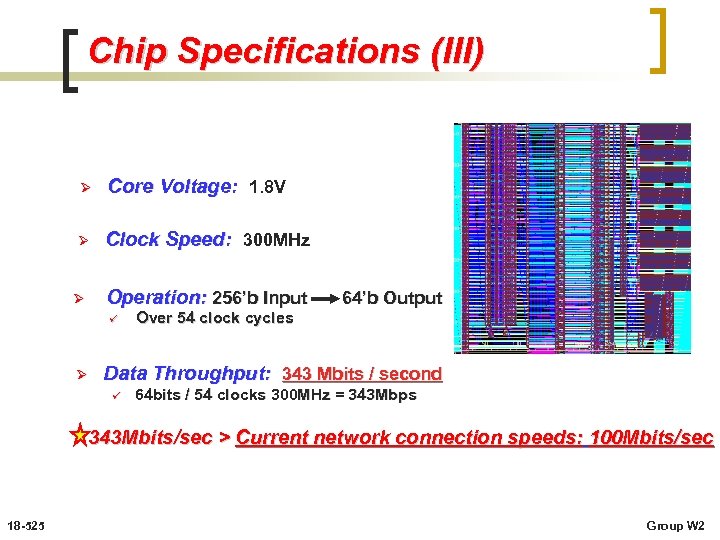
Chip Specifications (III) Ø Core Voltage: 1. 8 V Ø Clock Speed: 300 MHz Operation: 256’b Input Ø ü Ø 64’b Output Over 54 clock cycles Data Throughput: 343 Mbits / second ü 64 bits / 54 clocks 300 MHz = 343 Mbps 343 Mbits/sec > Current network connection speeds: 100 Mbits/sec 18 -525 Group W 2
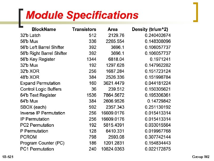
Module Specifications 18 -525 Group W 2
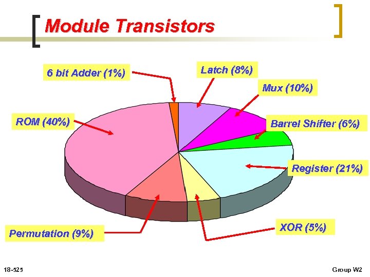
Module Transistors 6 bit Adder (1%) Latch (8%) Mux (10%) ROM (40%) Barrel Shifter (6%) Register (21%) Permutation (9%) 18 -525 XOR (5%) Group W 2
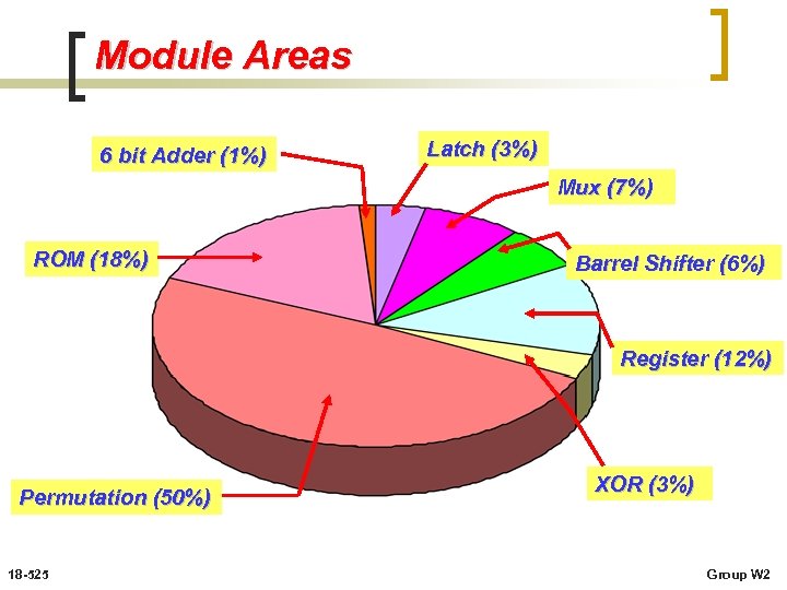
Module Areas 6 bit Adder (1%) Latch (3%) Mux (7%) ROM (18%) Barrel Shifter (6%) Register (12%) Permutation (50%) 18 -525 XOR (3%) Group W 2
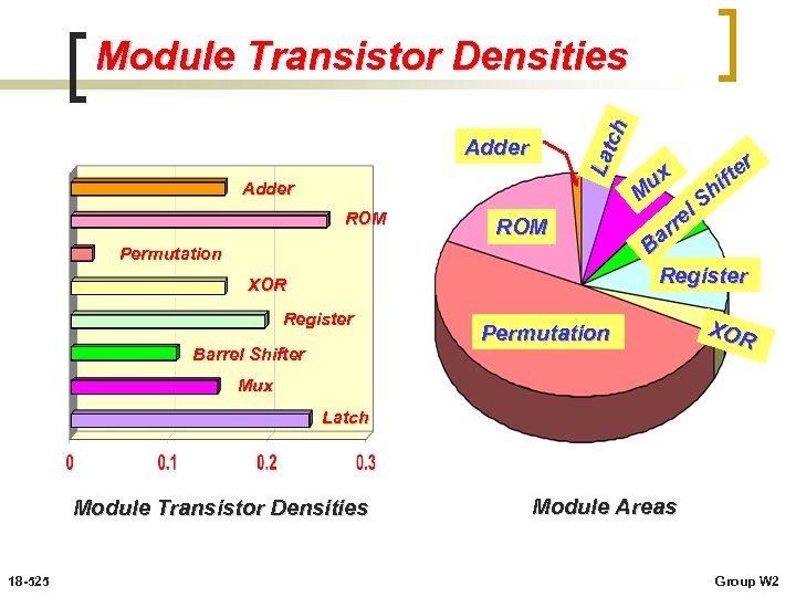
Lat ch Module Transistor Densities Adder ROM Permutation XOR Register Barrel Shifter r te f hi S el r ar B Register ux M Permutation XOR Mux Latch Module Transistor Densities 18 -525 Module Areas Group W 2
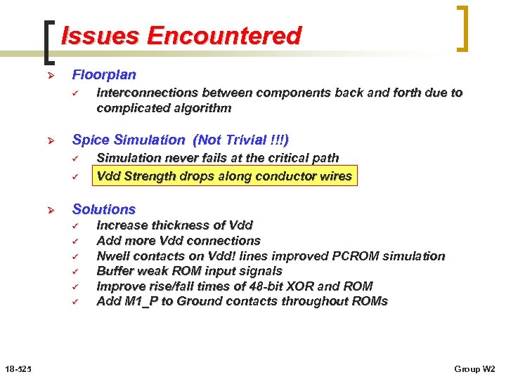
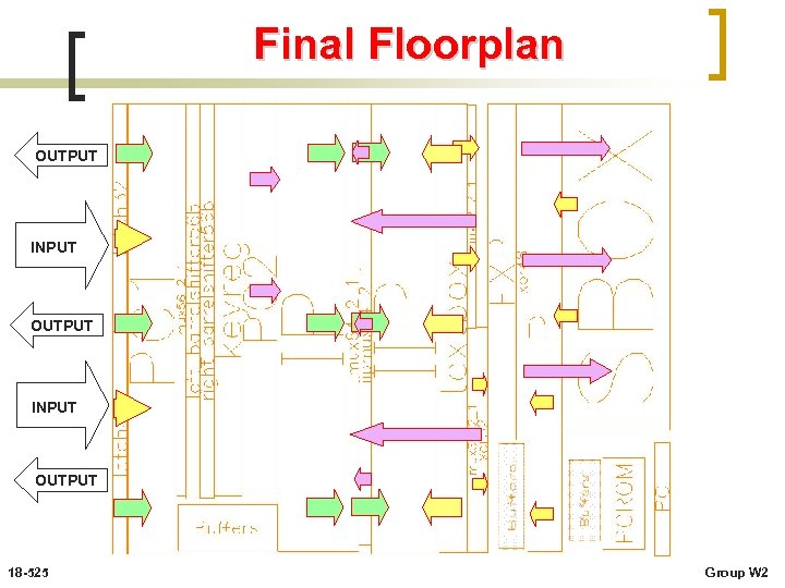
Issues Encountered Ø Floorplan ü Ø Spice Simulation (Not Trivial !!!) ü ü Ø Simulation never fails at the critical path Vdd Strength drops along conductor wires Solutions ü ü ü 18 -525 Interconnections between components back and forth due to complicated algorithm Increase thickness of Vdd Add more Vdd connections Nwell contacts on Vdd! lines improved PCROM simulation Buffer weak ROM input signals Improve rise/fall times of 48 -bit XOR and ROM Add M 1_P to Ground contacts throughout ROMs Group W 2
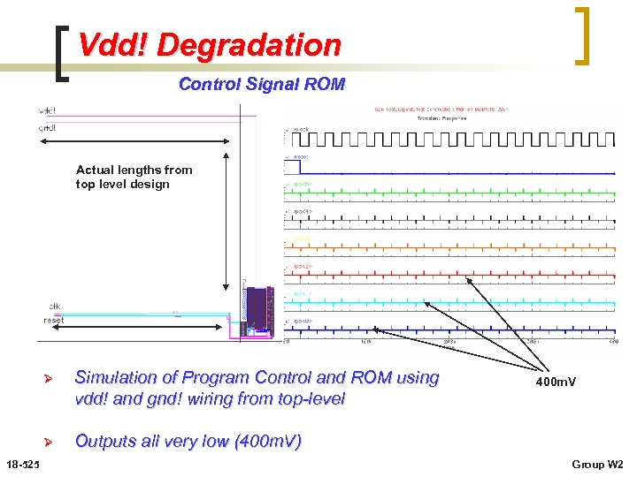
Vdd! Degradation Control Signal ROM Actual lengths from top level design Ø Ø 18 -525 Simulation of Program Control and ROM using vdd! and gnd! wiring from top-level Outputs all very low (400 m. V) 400 m. V Group W 2
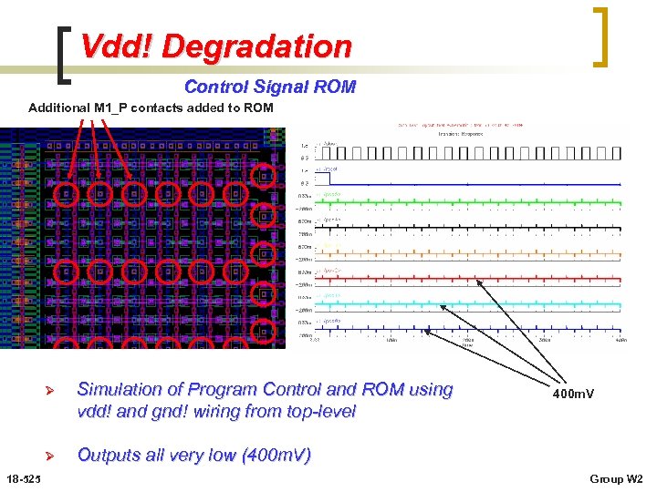
Vdd! Degradation Control Signal ROM Additional M 1_P contacts added to ROM Ø Ø 18 -525 Simulation of Program Control and ROM using vdd! and gnd! wiring from top-level Outputs all very low (400 m. V) 400 m. V Group W 2
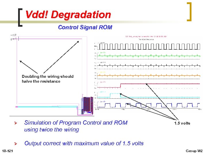
Vdd! Degradation Control Signal ROM Doubling the wiring should halve the resistance Ø Ø 18 -525 Simulation of Program Control and ROM using twice the wiring Output correct with maximum value of 1. 5 volts Group W 2
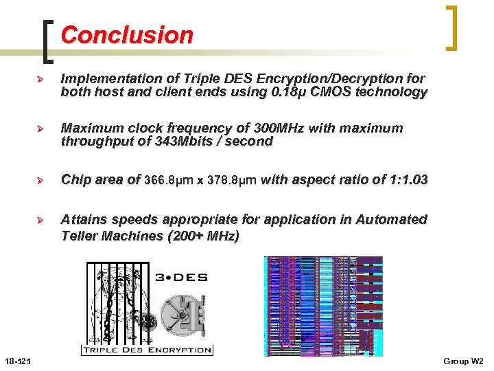
Conclusion Ø Ø Maximum clock frequency of 300 MHz with maximum throughput of 343 Mbits / second Ø Chip area of 366. 8μm x 378. 8μm with aspect ratio of 1: 1. 03 Ø 18 -525 Implementation of Triple DES Encryption/Decryption for both host and client ends using 0. 18μ CMOS technology Attains speeds appropriate for application in Automated Teller Machines (200+ MHz) Group W 2
f688ad1284122460b013f96fd4a1704e.ppt