Reviews.pptx
- Количество слайдов: 58

Embedded Systems Review Xu, Guangping xugp 2008@aliyun. com Tianjin University of Tech.

Part 1. BASICS
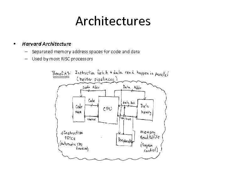
Architectures • Harvard Architecture – Separated memory address spaces for code and data – Used by most RISC processors
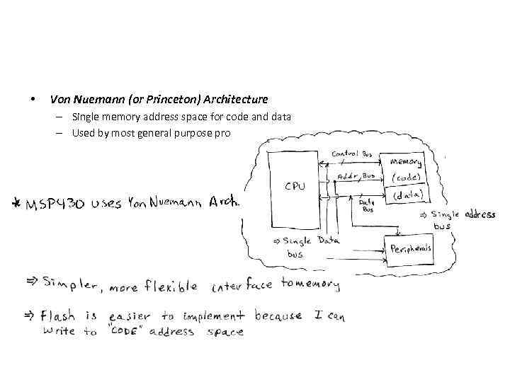
• Von Nuemann (or Princeton) Architecture – Single memory address space for code and data – Used by most general purpose processors
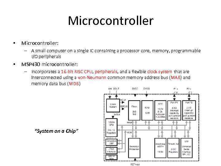
Microcontroller • Microcontroller: – A small computer on a single IC containing a processor core, memory, programmable I/O peripherals • MSP 430 microcontroller: – Incorporates a 16‐bit RISC CPU, peripherals, and a flexible clock system that are interconnected using a von‐Neumann common memory address bus (MAB) and memory data bus (MDB) “System on a Chip”
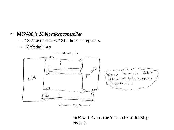
• MSP 430 is 16 bit microcontroller – 16 bit word size => 16 bit internal registers – 16 bit data bus RISC with 27 instructions and 7 addressing modes
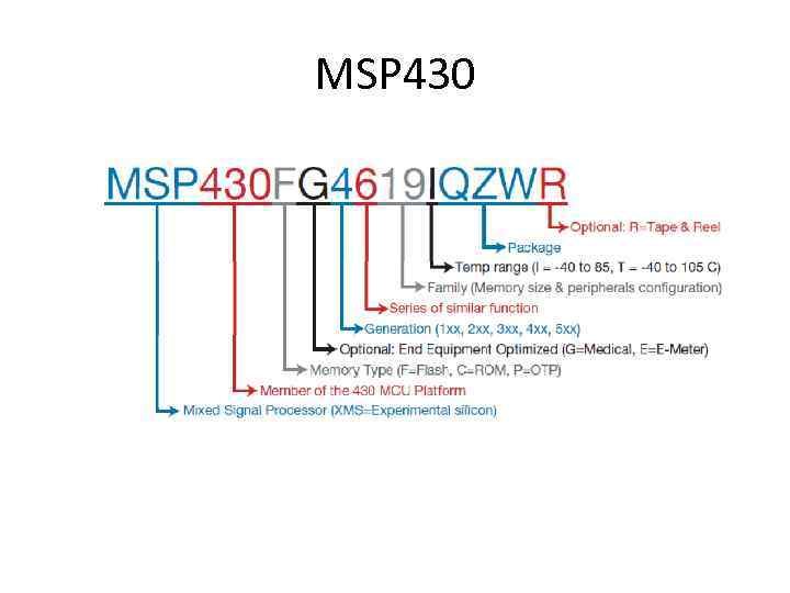
MSP 430
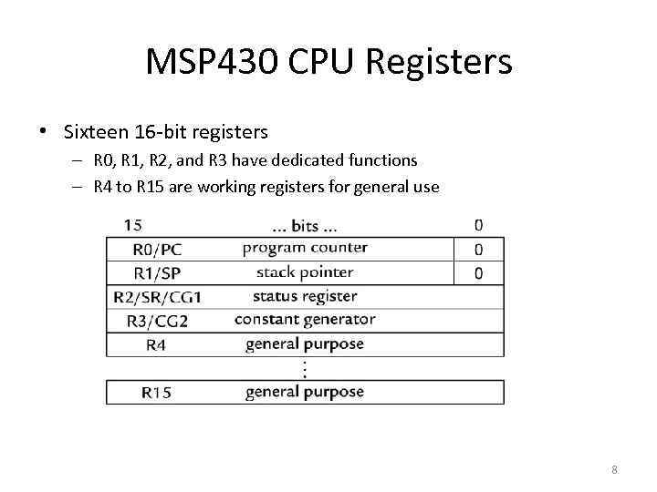
MSP 430 CPU Registers • Sixteen 16‐bit registers – R 0, R 1, R 2, and R 3 have dedicated functions – R 4 to R 15 are working registers for general use 8
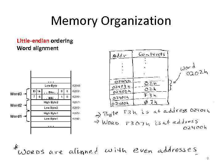
Memory Organization Little-endian ordering Word alignment Aligned words: The address of a word is the address of the byte with the lower address, which is even. 9
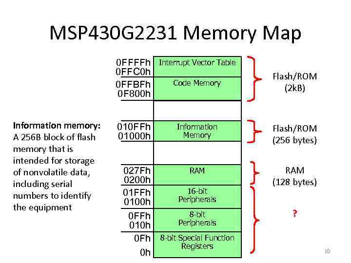
MSP 430 G 2231 Memory Map 0 FFFFh 0 FFC 0 h 0 FFBFh 0 F 800 h Information memory: A 256 B block of flash memory that is intended for storage of nonvolatile data, including serial numbers to identify the equipment Interrupt Vector Table Code Memory Flash/ROM (2 k. B) 010 FFh 01000 h Information Memory Flash/ROM (256 bytes) RAM (128 bytes) 027 Fh 0200 h 01 FFh 0100 h 0 FFh 010 h 0 Fh 0 h 16 -bit Peripherals 8 -bit Special Function Registers ? 10
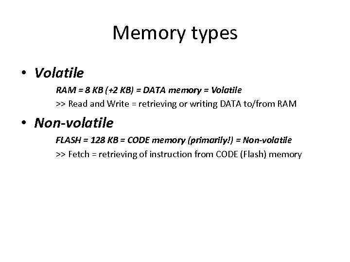
Memory types • Volatile RAM = 8 KB (+2 KB) = DATA memory = Volatile >> Read and Write = retrieving or writing DATA to/from RAM • Non-volatile FLASH = 128 KB = CODE memory (primarily!) = Non-volatile >> Fetch = retrieving of instruction from CODE (Flash) memory

Part 2. GPIO
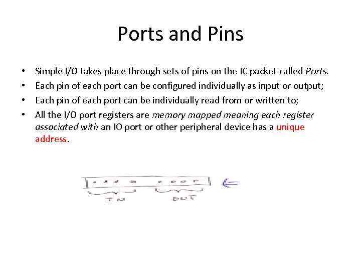
Ports and Pins • • Simple I/O takes place through sets of pins on the IC packet called Ports. Each pin of each port can be configured individually as input or output; Each pin of each port can be individually read from or written to; All the I/O port registers are memory mapped meaning each register associated with an IO port or other peripheral device has a unique address.
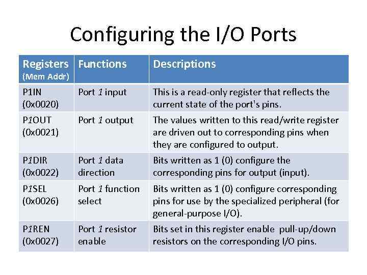
Configuring the I/O Ports Registers Functions Descriptions P 1 IN (0 x 0020) Port 1 input This is a read‐only register that reflects the current state of the port's pins. P 1 OUT (0 x 0021) Port 1 output The values written to this read/write register are driven out to corresponding pins when they are configured to output. P 1 DIR (0 x 0022) Port 1 data direction Bits written as 1 (0) configure the corresponding pins for output (input). P 1 SEL (0 x 0026) Port 1 function select Bits written as 1 (0) configure corresponding pins for use by the specialized peripheral (for general‐purpose I/O). P 1 REN (0 x 0027) Port 1 resistor enable Bits set in this register enable pull‐up/down resistors on the corresponding I/O pins. (Mem Addr)
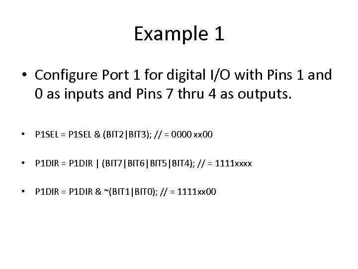
Example 1 • Configure Port 1 for digital I/O with Pins 1 and 0 as inputs and Pins 7 thru 4 as outputs. • P 1 SEL = P 1 SEL & (BIT 2|BIT 3); // = 0000 xx 00 • P 1 DIR = P 1 DIR | (BIT 7|BIT 6|BIT 5|BIT 4); // = 1111 xxxx • P 1 DIR = P 1 DIR & ~(BIT 1|BIT 0); // = 1111 xx 00
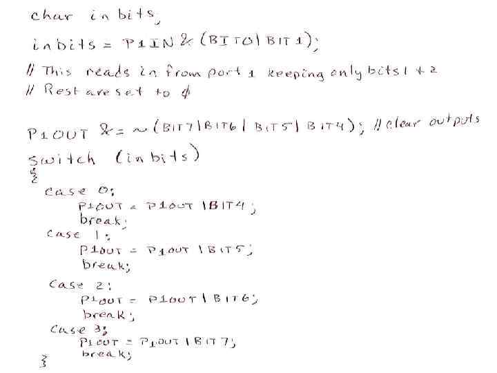
Example 2 • Read in from properly configured Port 1 Pins 1 and 0 and place a 1 on the outputs Pins 7~4 that correspond to the binary code 0~3.
Part 3. PROGRAMMING MODES
Two programming modes • Polling – It needs to regularly query the input status and react as appropriate. +: easy to implement and debug ‐: processor intensive if event is rare, you waste a lot of time checking processor can’t go into low power (slow or stopped) modes
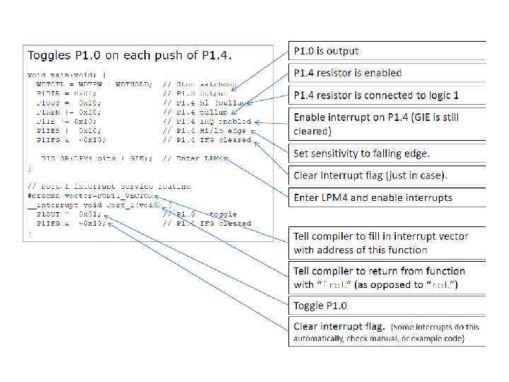
Two programming modes • Interrupts – The processor is “interrupted” by an event and responses it. +: very efficient time‐wise: no time wasted looking for an event that hasn’t occurred. +: very efficient energy‐wise: processor can be asleep most of the time. ‐: can be hard to debug
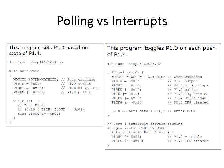
Polling vs Interrupts
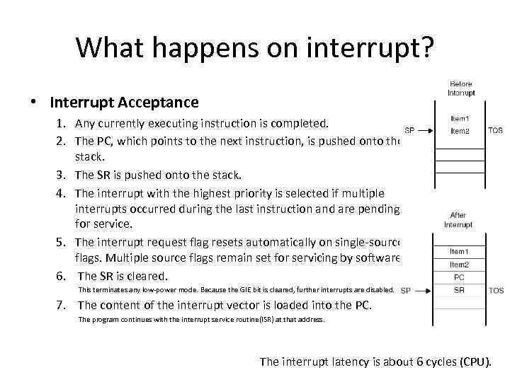
What happens on interrupt? • Interrupt Acceptance 1. Any currently executing instruction is completed. 2. The PC, which points to the next instruction, is pushed onto the stack. 3. The SR is pushed onto the stack. 4. The interrupt with the highest priority is selected if multiple interrupts occurred during the last instruction and are pending for service. 5. The interrupt request flag resets automatically on single‐source flags. Multiple source flags remain set for servicing by software. 6. The SR is cleared. This terminates any low‐power mode. Because the GIE bit is cleared, further interrupts are disabled. 7. The content of the interrupt vector is loaded into the PC. The program continues with the interrupt service routine(ISR) at that address. The interrupt latency is about 6 cycles (CPU).
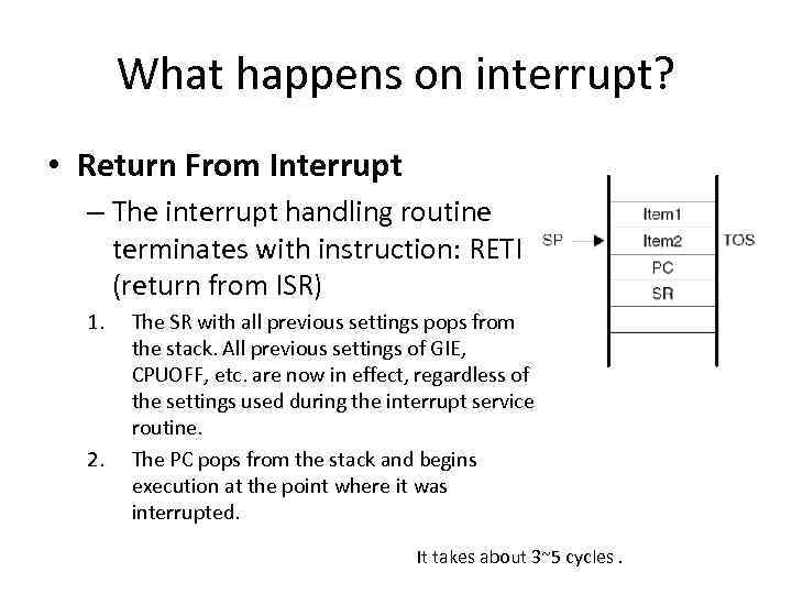
What happens on interrupt? • Return From Interrupt – The interrupt handling routine terminates with instruction: RETI (return from ISR) 1. 2. The SR with all previous settings pops from the stack. All previous settings of GIE, CPUOFF, etc. are now in effect, regardless of the settings used during the interrupt service routine. The PC pops from the stack and begins execution at the point where it was interrupted. It takes about 3~5 cycles.
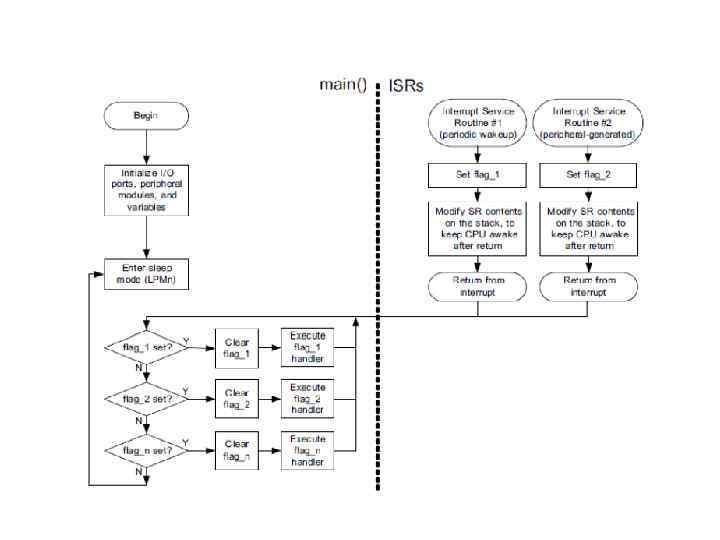
Keep ISR’s short! • It is important to keep interrupt service routines short. – Since interrupts are disable globally during an ISR, you might miss something important. • If you need to do a lot of processing, have the ISR set a flag, and have main routine act on it.
Part 4. CLOCK SYSTEMS
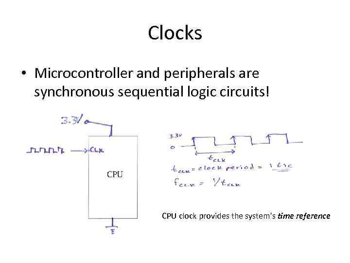
Clocks • Microcontroller and peripherals are synchronous sequential logic circuits! CPU clock provides the system's time reference
Requirements and Supplies • Two kinds of clocks often needed: – A fast clock to drive CPU, which can be started and stopped rapidly (lots of power used) but need not be particularly accurate. – A slow clock that runs continuously to monitor real time, which must use little power and be accurate. • Different clock sources also have different characteristics – Crystal: • accurate and stable (w. r. t. temperature or time); expensive, delicate, drawing large current, external component, longer time to start up/stabilize – Resistor and capacitor (RC): • cheap, quick to start, integrated within MCU and sleep with CPU; poor accuracy and stability
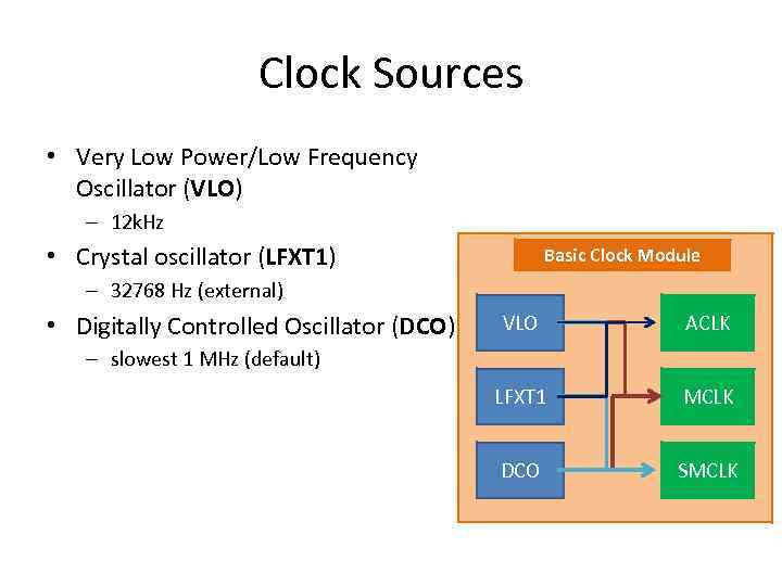
Clock Sources • Very Low Power/Low Frequency Oscillator (VLO) – 12 k. Hz • Crystal oscillator (LFXT 1) Basic Clock Module – 32768 Hz (external) • Digitally Controlled Oscillator (DCO) VLO ACLK LFXT 1 MCLK DCO SMCLK – slowest 1 MHz (default) 30
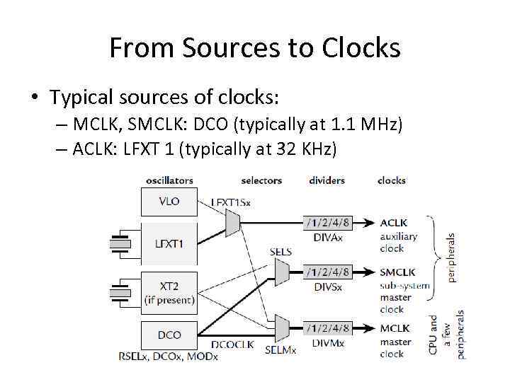
From Sources to Clocks • Typical sources of clocks: – MCLK, SMCLK: DCO (typically at 1. 1 MHz) – ACLK: LFXT 1 (typically at 32 KHz)
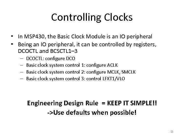
Controlling Clocks • In MSP 430, the Basic Clock Module is an IO peripheral • Being an IO peripheral, it can be controlled by registers, DCOCTL and BCSCTL 1– 3 – – DCOCTL: configure DCO Basic clock system control 1: configure ACLK Basic clock system control 2: configure MCLK, SMCLK Basic clock system control 3: control LFXT 1/VLO Engineering Design Rule = KEEP IT SIMPLE!! ->Use defaults when possible! 32 32

Part 5. TIMER
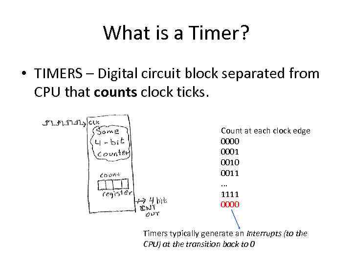
What is a Timer? • TIMERS – Digital circuit block separated from CPU that counts clock ticks. Count at each clock edge 0000 0001 0010 0011. . . 1111 0000 Timers typically generate an Interrupts (to the CPU) at the transition back to 0
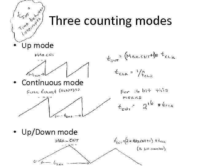
Three counting modes • Up mode • Continuous mode • Up/Down mode
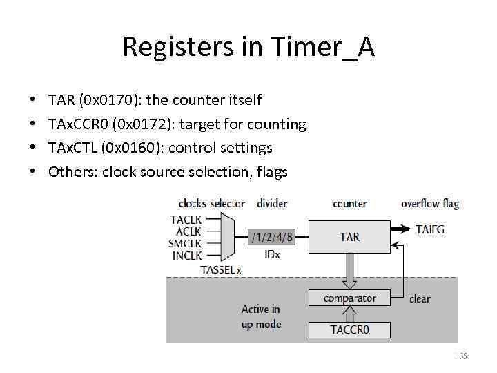
Registers in Timer_A • • TAR (0 x 0170): the counter itself TAx. CCR 0 (0 x 0172): target for counting TAx. CTL (0 x 0160): control settings Others: clock source selection, flags 36 36
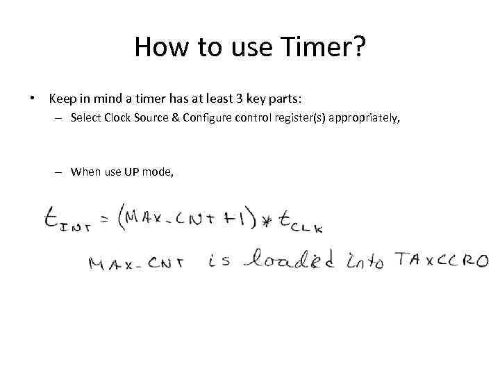
How to use Timer? • Keep in mind a timer has at least 3 key parts: – Select Clock Source & Configure control register(s) appropriately, – When use UP mode,
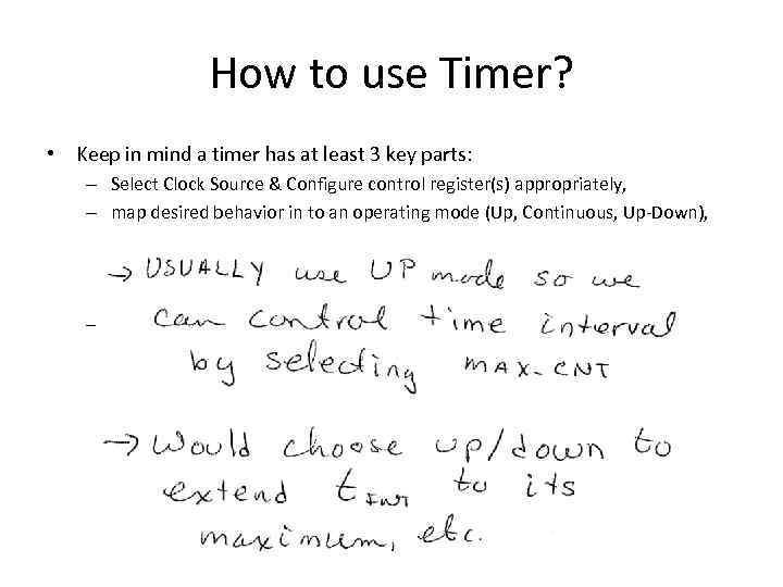
How to use Timer? • Keep in mind a timer has at least 3 key parts: – Select Clock Source & Configure control register(s) appropriately, – map desired behavior in to an operating mode (Up, Continuous, Up‐Down), – Write Interrupt Service Routines (ISR) and enable interrupts.
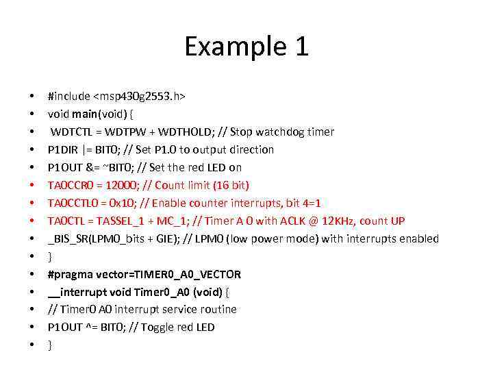
Example 1 • • • • #include <msp 430 g 2553. h> void main(void) { WDTCTL = WDTPW + WDTHOLD; // Stop watchdog timer P 1 DIR |= BIT 0; // Set P 1. 0 to output direction P 1 OUT &= ~BIT 0; // Set the red LED on TA 0 CCR 0 = 12000; // Count limit (16 bit) TA 0 CCTL 0 = 0 x 10; // Enable counter interrupts, bit 4=1 TA 0 CTL = TASSEL_1 + MC_1; // Timer A 0 with ACLK @ 12 KHz, count UP _BIS_SR(LPM 0_bits + GIE); // LPM 0 (low power mode) with interrupts enabled } #pragma vector=TIMER 0_A 0_VECTOR __interrupt void Timer 0_A 0 (void) { // Timer 0 A 0 interrupt service routine P 1 OUT ^= BIT 0; // Toggle red LED }
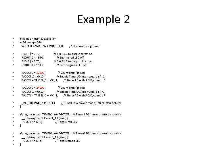
Example 2 • • • #include <msp 430 g 2553. h> void main(void) { WDTCTL = WDTPW + WDTHOLD; // Stop watchdog timer • • P 1 DIR |= BIT 0; // Set P 1. 0 to output direction P 1 OUT &= ~BIT 0; // Set the red LED off P 1 DIR |= BIT 6; // Set P 1. 6 to output direction P 1 OUT &= ~BIT 6; // Set the green LED off • • • TA 0 CCR 0 = 12000; // Count limit (16 bit) TA 0 CCTL 0 = 0 x 10; // Enable Timer A 0 interrupts, bit 4=1 TA 0 CTL = TASSEL_1 + MC_1; // Timer A 0 with ACLK, count UP • • • TA 1 CCR 0 = 24000; // Count limit (16 bit) TA 1 CCTL 0 = 0 x 10; // Enable Timer A 1 interrupts, bit 4=1 TA 1 CTL = TASSEL_1 + MC_1; // Timer A 1 with ACLK, count UP • • _BIS_SR(LPM 0_bits + GIE); // LPM 0 (low power mode) interrupts enabled } • • #pragma vector=TIMER 1_A 0_VECTOR // Timer 1 A 0 interrupt service routine __interrupt void Timer 1_A 0 (void) { P 1 OUT ^= BIT 0; // Toggle red LED } • • #pragma vector=TIMER 0_A 0_VECTOR // Timer 0 A 0 interrupt service routine __interrupt void Timer 0_A 0 (void) { P 1 OUT ^= BIT 6; // Toggle green LED }
Detailed Example • Implement a stop watch that measures seconds and hundredths of seconds using Timer A 0.

1. How will we measure the passage of 0. 01 seconds?
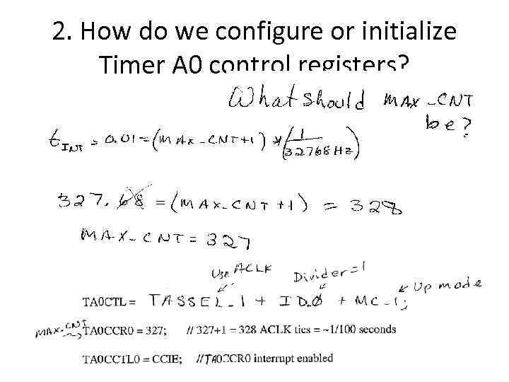
2. How do we configure or initialize Timer A 0 control registers?
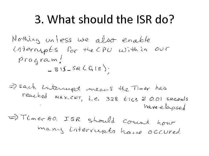
3. What should the ISR do?
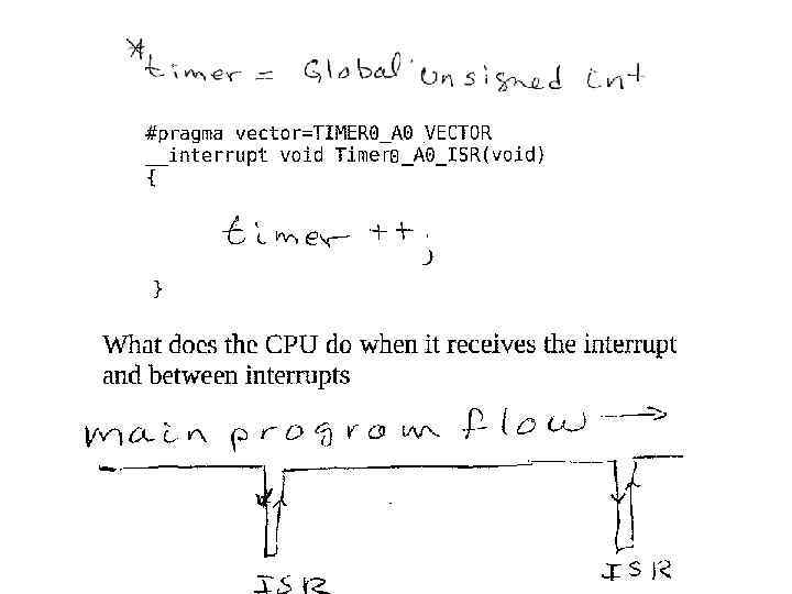

Part 6. LOWER POWER MODES
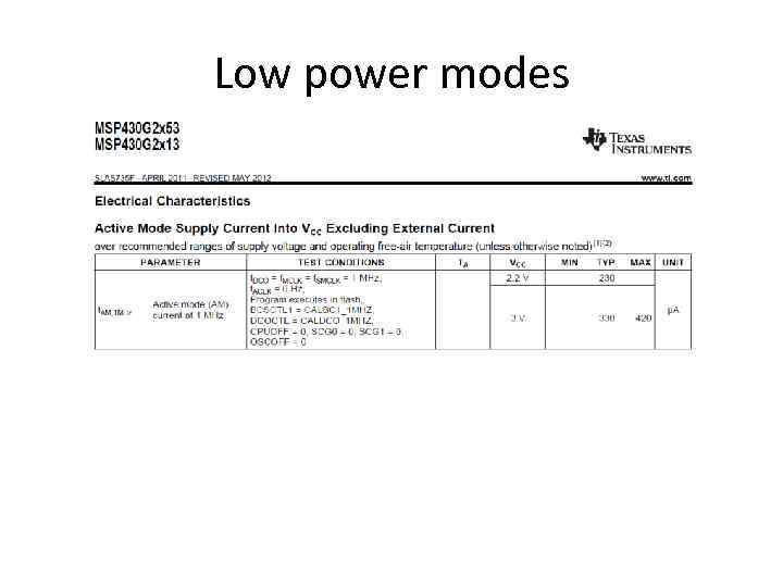
Low power modes
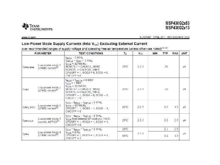

Energy Savings • Alkaline AAA Batteries – Rated as 1100 m. A/hr
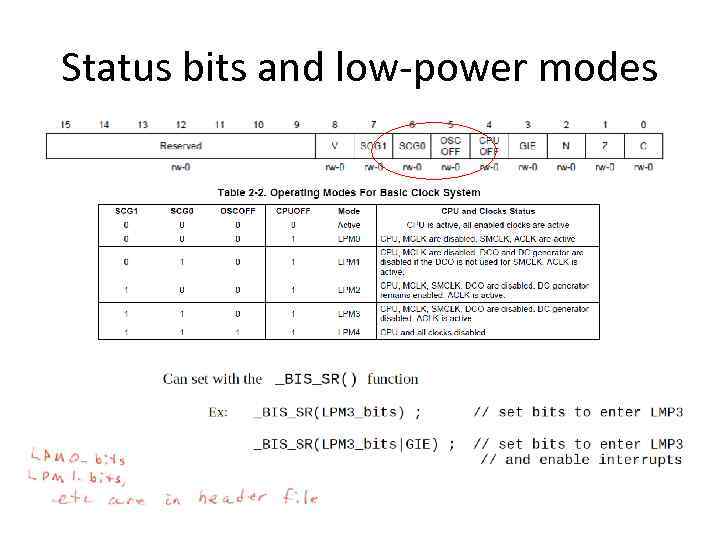
Status bits and low‐power modes
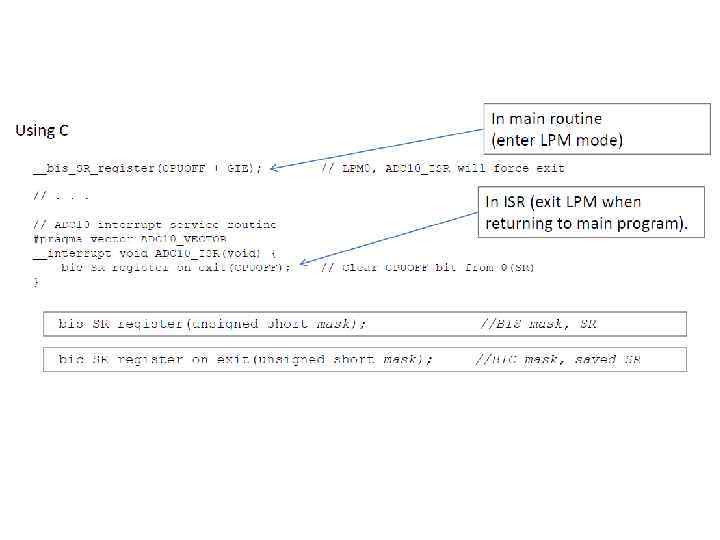
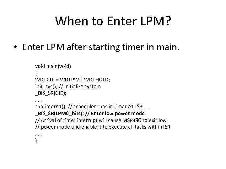
When to Enter LPM? • Enter LPM after starting timer in main. void main(void) { WDTCTL = WDTPW | WDTHOLD; init_sys(); // initialize system _BIS_SR(GIE); . . . runtimer. A 1(); // scheduler runs in timer A 1 ISR. . . _BIS_SR(LPM 0_bits); // Enter low power mode // Arrival of timer interrupt will cause MSP 430 to exit low // power mode and enable it to execute all tasks within ISR. . . }
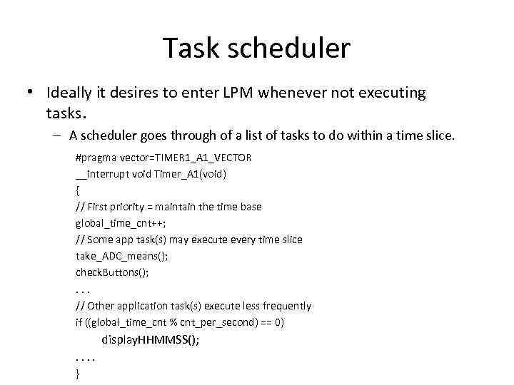
Task scheduler • Ideally it desires to enter LPM whenever not executing tasks. – A scheduler goes through of a list of tasks to do within a time slice. #pragma vector=TIMER 1_A 1_VECTOR __interrupt void Timer_A 1(void) { // First priority = maintain the time base global_time_cnt++; // Some app task(s) may execute every time slice take_ADC_means(); check. Buttons(); . . . // Other application task(s) execute less frequently if ((global_time_cnt % cnt_per_second) == 0) display. HHMMSS(); . . }
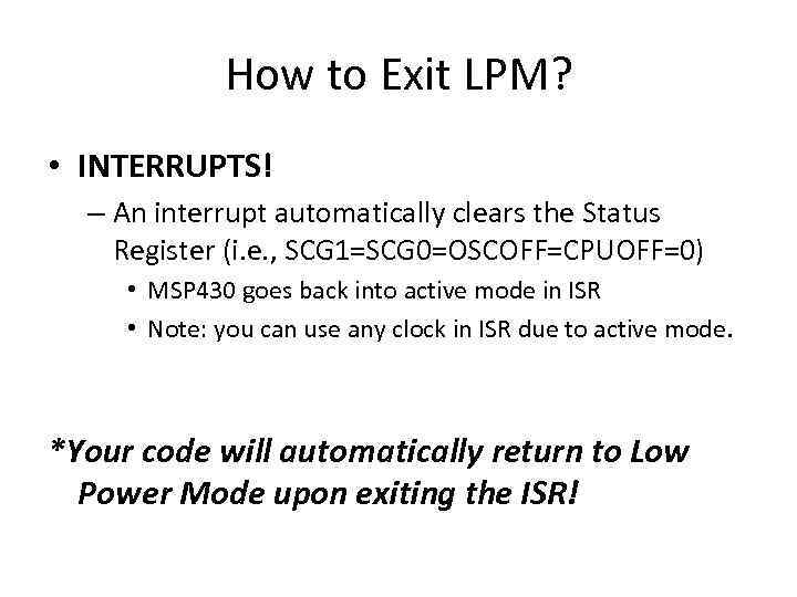
How to Exit LPM? • INTERRUPTS! – An interrupt automatically clears the Status Register (i. e. , SCG 1=SCG 0=OSCOFF=CPUOFF=0) • MSP 430 goes back into active mode in ISR • Note: you can use any clock in ISR due to active mode. *Your code will automatically return to Low Power Mode upon exiting the ISR!
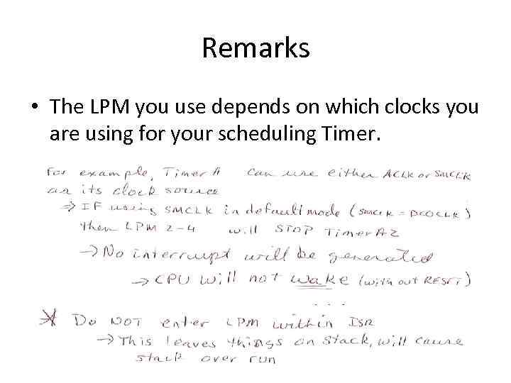
Remarks • The LPM you use depends on which clocks you are using for your scheduling Timer.

ADC

COMMUNICATION

Part VI. WATCH DOGS
Reviews.pptx