b847eccdd9df9a107c4583b87a9273c9.ppt
- Количество слайдов: 31
 Electronics for the Liquid Scintillator OA Detector Option Alfons Weber Feb 2004 with help from: ANL, Cambridge, FNAL, Harvard, RAL, UMN
 Jan 2004 2 System Overview n Physics Specifications n n n APDs FE chip n n Measurements (Leon) Readout Architecture n n light level, noise Analogue or digital pipeline DAQ system Timing System R&D for the next year
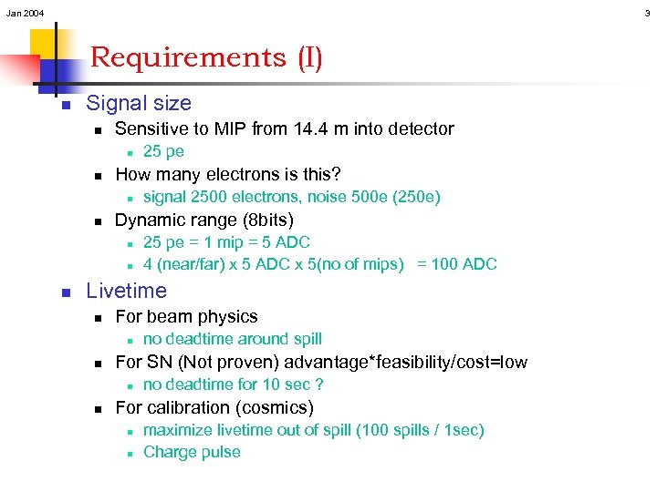 Jan 2004 3 Requirements (I) n Signal size n Sensitive to MIP from 14. 4 m into detector n n How many electrons is this? n n signal 2500 electrons, noise 500 e (250 e) Dynamic range (8 bits) n n n 25 pe = 1 mip = 5 ADC 4 (near/far) x 5 ADC x 5(no of mips) = 100 ADC Livetime n For beam physics n n For SN (Not proven) advantage*feasibility/cost=low n n no deadtime around spill no deadtime for 10 sec ? For calibration (cosmics) n n maximize livetime out of spill (100 spills / 1 sec) Charge pulse
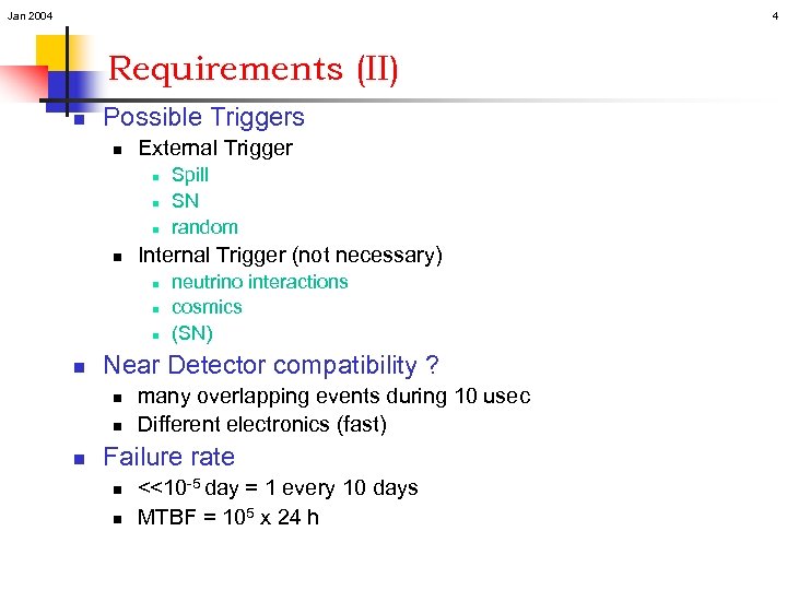 Jan 2004 4 Requirements (II) n Possible Triggers n External Trigger n n Internal Trigger (not necessary) n n neutrino interactions cosmics (SN) Near Detector compatibility ? n n n Spill SN random many overlapping events during 10 usec Different electronics (fast) Failure rate n n <<10 -5 day = 1 every 10 days MTBF = 105 x 24 h
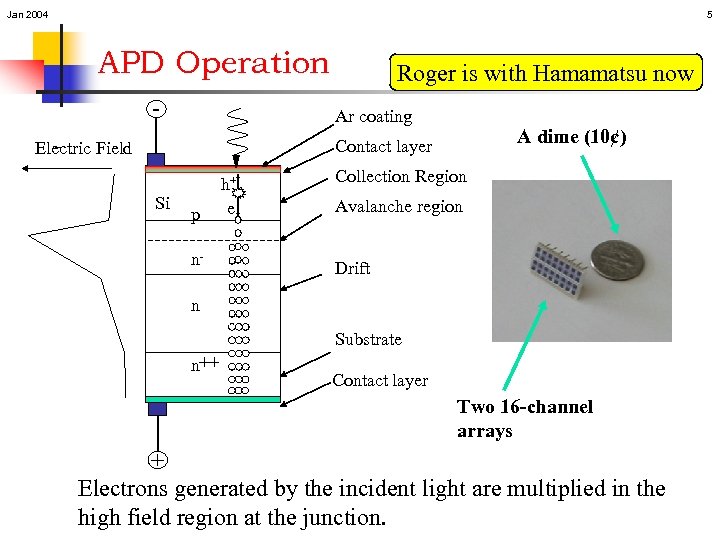 Jan 2004 5 APD Operation - Roger is with Hamamatsu now Ar coating A dime (10¢) Contact layer Electric Field Si p n- h+ e Collection Region Avalanche region Drift n Substrate n++ Contact layer Two 16 -channel arrays + Electrons generated by the incident light are multiplied in the high field region at the junction.
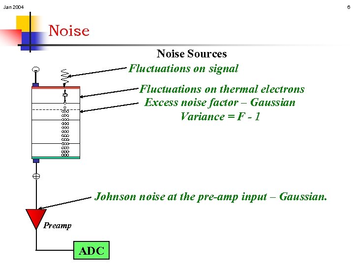 Jan 2004 6 Noise Sources Fluctuations on signal - Fluctuations on thermal electrons Excess noise factor – Gaussian Variance = F - 1 + Johnson noise at the pre-amp input – Gaussian. Preamp ADC
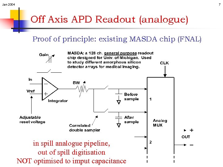 Jan 2004 7 Off Axis APD Readout (analogue) Proof of principle: existing MASDA chip (FNAL) in spill analogue pipeline, out of spill digitisation NOT optimised to imput capacitance
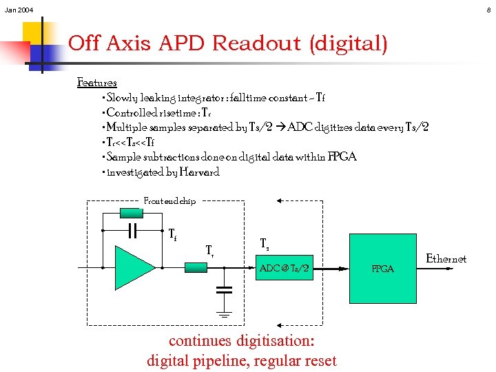 Jan 2004 8 Off Axis APD Readout (digital) Features • Slowly leaking integrator : falltime constant - Tf • Controlled risetime : Tr • Multiple samples separated by Ts/2 ADC digitizes data every Ts/2 • Tr<
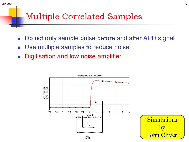 Jan 2004 9 Multiple Correlated Samples n n n Do not only sample pulse before and after APD signal Use multiple samples to reduce noise Digitisation and low noise amplifier Ts 3 Ts Simulations by John Oliver
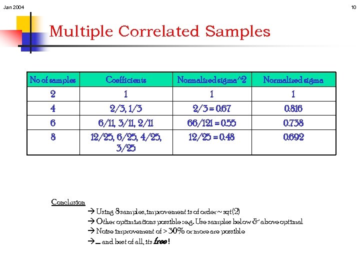 Jan 2004 10 Multiple Correlated Samples No of samples Coefficients Normalized sigma^2 Normalized sigma 2 1 1 1 4 2/3, 1/3 2/3 = 0. 67 0. 816 6 6/11, 3/11, 2/11 66/121 = 0. 55 0. 738 8 12/25, 6/25, 4/25, 3/25 12/25 = 0. 48 0. 692 Conclusion Using 8 samples, improvement is of order ~ sqt(2) Other optimizations possible : e. g. Use samples below & above optimal Noise improvement of > 30% or more are possible …. . and best of all, its free !
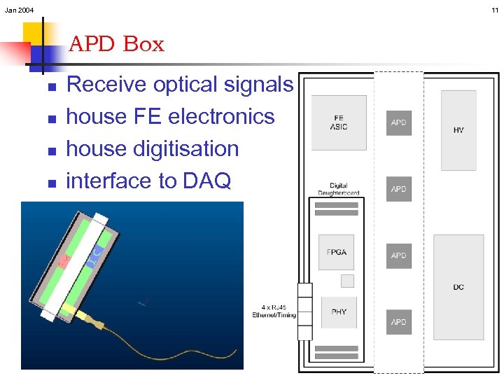 Jan 2004 11 APD Box n n Receive optical signals house FE electronics house digitisation interface to DAQ
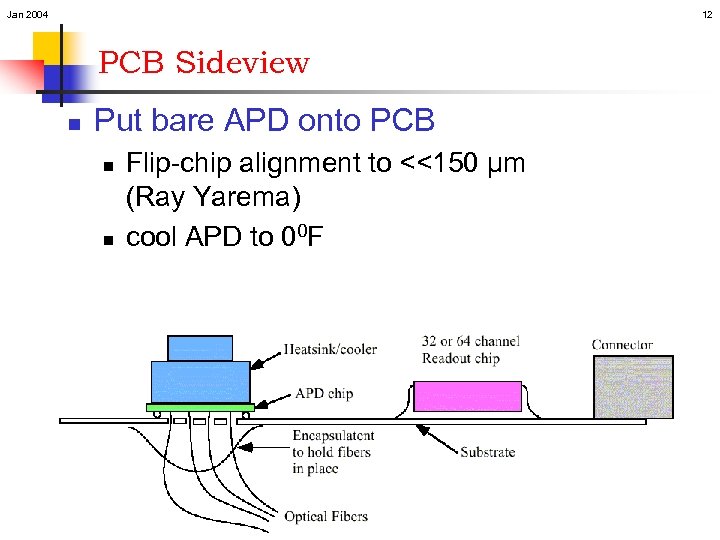 Jan 2004 12 PCB Sideview n Put bare APD onto PCB n n Flip-chip alignment to <<150 μm (Ray Yarema) cool APD to 00 F
 Jan 2004 13 APD Box (II) n n n Difficult! Needs dedicated electro-mechanical engineering (FNAL, UMN) To be considered: n n n optical & digital & LV connections light tight condensation noise insulation (external & digital) heat load from cooled APDs …
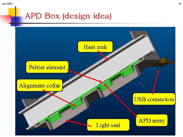 Jan 2004 14 APD Box (design idea) Heat sink Peltier element Alignment collar USB connection Light seal APD array
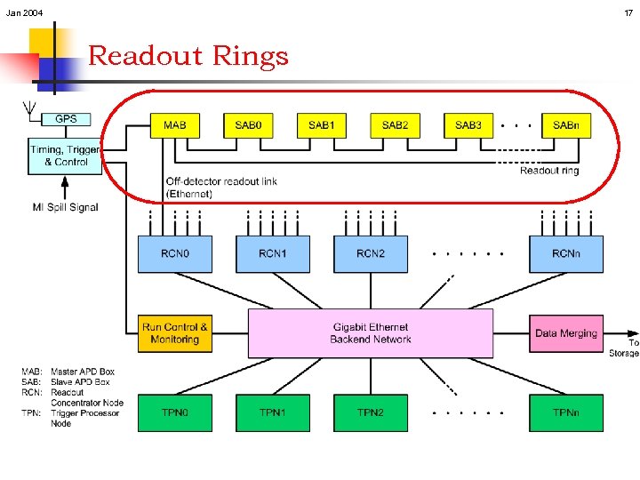
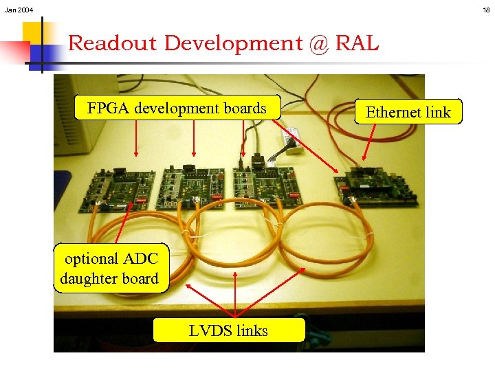
 Jan 2004 15 DAQ System (RAL) n n Readout/DAQ is cost sensitive item Want: n n n n n Low cost per channel Scalable, flexible system Minimise off-detector links (major cost item) Use standard technology where possible Future upgrade paths considered Aggregate data from multiple APD boxes (96) Use (Gbit) Ethernet for off-detector links Total throughput scales with increased links COTS technology for DAQ backend
 Jan 2004 16 Input constraints n 10, 000 APD boxes n n 64 channels / box (2 scintillator modules) 8 Byte/channel @ 2 MHz n n n Continuous sampling, but ZERO suppressed Assume spill = 20 µs Data rate n n n Noise: 10 -3 x 2 MHz x 8 Byte, Signal: 0 Hz 1 MB/s per APD box = 10 GB/s total raw data rate 20 bytes per spill per APD box 200 k. Bytes per spill 100 Hz readout rate = 20 MB/s total rate
 Jan 2004 17 Readout Rings
 Jan 2004 18 Readout Development @ RAL FPGA development boards optional ADC daughter board LVDS links Ethernet link
 Jan 2004 Readout Concentrator Node PC with several network cards 19
 Jan 2004 DAQ Backend PC with Gigabit Ethernet 20
 Jan 2004 21 Clock & Timing System n n FE needs timing to be synchronised across the detector FE may need accurate spill signal n n in time: analogue pipeline not to late: digital pipeline Need to get spill signal from FNAL to OA site Need to distribute clock around the detector.
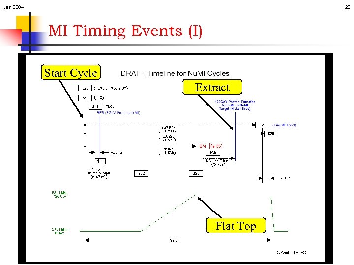 Jan 2004 22 MI Timing Events (I) Start Cycle Extract Flat Top
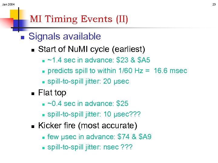 Jan 2004 23 MI Timing Events (II) n Signals available n Start of Nu. MI cycle (earliest) n n Flat top n n n ~1. 4 sec in advance: $23 & $A 5 predicts spill to within 1/60 Hz = 16. 6 msec spill-to-spill jitter: 20 µsec ~0. 4 sec in advance: $25 spill-to-spill jitter: 10 µsec? ? ? Kicker fire (most accurate) n n few µsec in advance: $74 & $A 9 spill-to-spill jitter: nsec ? ? ?
 Jan 2004 24 Signal Transmission n Conventional HEP timing signal distribution at OA site But: How do we get the spill signal to the detector? Options: n n n Internet (slow, ~0. 5 sec latency ? ) Phone line (fast, msec latency) Dedicated radio transmitter (fast)
 Jan 2004 25 R&D Plans for FY 04. n Objectives: n Demonstrate readout of 14. 5 m long strip with cooled APD. n n n Design and cost APD readout box n n Build ~ 5 readout boxes with un-optimized Mazda chip and packaged APD’s – analog store Build 1 prototype readout box with digital store. Design for manufacturability. Thermal, optical and electrical. Refine system cost estimate. DAQ specification.
 Jan 2004 26 R&D in 2004 - Deliverables n Readout Modules for readout of 14. 4 m tubes. n n n Engineering and Design. n n n analogue pipeline (MASDA) digital pipeline Gbit Ethernet on FPGA Clock & Timing system APD box Power distribution system Detailed system cost estimate.
 Jan 2004 27
 Jan 2004 28 APD Box Functions (SAB) n Slave and Master APD Box n n n Receive clock/spill signal Digitise/timestamp APD signals Sparcify data (zero suppression) Transmit data for “spill” on request All implemented in FPGA (firmware) Master APD Box only n n n Receive clock/ctrl signals from timing system Re-transmit clock/ctrl on SAB ring Read out SAB via ring n n n SABs are daisy-chained Ring architecture: each SAB can be accessed on either leg Redundancy: save against single SAB failure Encapsulate data and transmit it to Readout Concentration Node 95 SAB are read out by one MAB (8 planes)
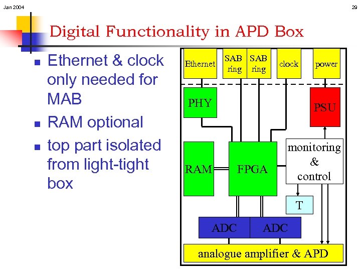 Jan 2004 29 Digital Functionality in APD Box n n n Ethernet & clock only needed for MAB RAM optional top part isolated from light-tight box Ethernet SAB ring clock PHY RAM power PSU FPGA monitoring & control T ADC analogue amplifier & APD
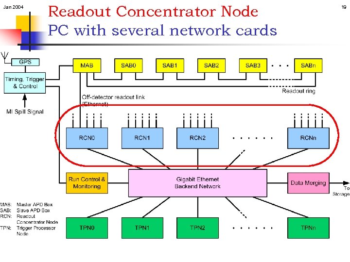
 Jan 2004 30 Readout Concentrator Node (RCN) n RCN is a standard PC n n In Spill mode: n n with several network cards Receive data from several 4 -16 MABs over Ethernet, i. e. 8 RCNs needed Traffic shaping and buffering Transmit data to Trigger Processing Nodes Also in self-triggering mode (only): n n Receive trigger primitives/Make L 1 trigger decision Broadcast trigger time to MABs & other RCN Receive data for trigger time More RCNs possible
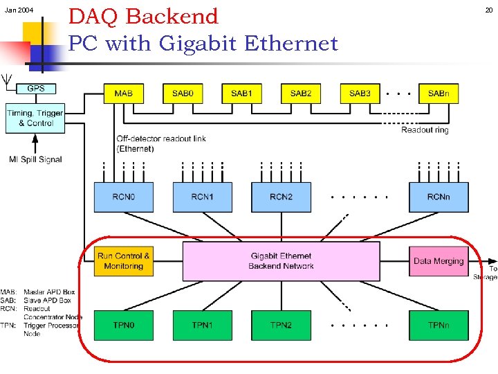
 Jan 2004 31 Trigger Farm / Data Merging n One Master RCN n n coordinating transfer of data to trigger farm Trigger Processing Nodes (TPNs) n n All detector data together for the first time Run S/W trigger algorithm(s) to identify events n n n Cosmics Beam events ? ? ? Data Merging node takes data from TPNs for storage Can easily take many spill triggers / sec


