

b7cfba95f9176dd0992ad8fc8d23a863.ppt
- Количество слайдов: 95
 Electronic Presentation Guide 18 th International Conference on VLSI Design Conference Kolkata, 2005 05/18/01 V 4. 3
 The vision: Ambient Inteligence Devices as Appliances On-Body Ad-hoc Sensor Adaptive Wireless In-Home • Power efficiency is one cornerstone of ambient intelligence • Flexibility and adaptability are another
 The AMI processing Bestiary • The work-horse – Powers the fixed base network machines – Power W Performance GB/s • The hummingbird – Powers the wireless base network interfaces – Power m. W Performance MB/s • The butterfly – The sensor network hardware – Power µW Performance KB/s
") Workhorse: Itanium® II Processor • • l l L 3 CACHE (1. 5/3 MB) Released at 733 MHz and 800 MHz, now 1 GHz Three level caching system 25 million transistors in the CPU and 300 million in the cache (0. 18µm) 421 mm 2 die size The CPU running at full load draws ~130 Watts The clock signals and logic total to approx 84% of the total power usage. Leakage power: approx. 2%. Power delivery: Vdd=1. 5 V, P=130 W, P=Vdd. I (!!)
Workhorse: Itanium® II Processor • • l l L 3 CACHE (1. 5/3 MB) Released at 733 MHz and 800 MHz, now 1 GHz Three level caching system 25 million transistors in the CPU and 300 million in the cache (0. 18µm) 421 mm 2 die size The CPU running at full load draws ~130 Watts The clock signals and logic total to approx 84% of the total power usage. Leakage power: approx. 2%. Power delivery: Vdd=1. 5 V, P=130 W, P=Vdd. I (!!)
 Hummingbird: TMS 320 vc 5471 • • C 540 • • ARM 7 • Core Vdd=1. 8 V, I/O Vdd=3. 3 V Power (f. ARM=50 MHz, f. DSP=100 MHz) = 291 m. W – Core 126 m. W – I/O 165 m. W 2 K 16 -bit 2 -ported DSPARM sh-mem interface 72 K for DSP, 16 KB for ARM DMA, UART, IRDA, Ethernet…
 Pad to Photodiode CCR Vdd Pad GND Power-on Reset Pad/ LFSR 300µm Charge Pump Butterfly: Berkeley’s Daft Dust 360µm • 63 mm 3 • Circuits: 0. 25 µm CMOS – digital circuits underneath ground pad – metal shields to prevent photogenerated carriers • Power consumption ~50µW (? )
 The Energy-Flexibility Tradeoff 1000 10 1 Dedicated") Energy Efficiency MOPS/m. W (or MIPS/m. W) The Energy-Flexibility Tradeoff 1000 10 1 Dedicated HW Reconfigurable Processor/Logic ASIPs DSPs Programmable solutions When? Always! Where? Everywhere! 10 -80 MOPS/m. W 2 V DSP: 3 MOPS/m. W Embedded Processors 0. 4 MIPS/m. W 0. 1 Flexibility (Coverage)
Energy Efficiency MOPS/m. W (or MIPS/m. W) The Energy-Flexibility Tradeoff 1000 10 1 Dedicated HW Reconfigurable Processor/Logic ASIPs DSPs Programmable solutions When? Always! Where? Everywhere! 10 -80 MOPS/m. W 2 V DSP: 3 MOPS/m. W Embedded Processors 0. 4 MIPS/m. W 0. 1 Flexibility (Coverage)
 Dynamic Energy Consumption Vdd Vin Vout CL Energy/transition = CL * VDD 2 * P 0 1
 Leakage Energy Vout OFF Gate leakage Drain junction leakage Sub-threshold current Independent of switching
 Leakage Current Mechanisms I 1 p-n junction reverse bias current I 7 I 8 Polysilicon Gate oxide Source Drain n+ n+ I 2 I 3 I 6 I 5 I 4 p substrate Bulk (Body) I 1 I 2 weak inversion (subthreshold) I 3 DIBL I 4 GIDL I 5 punchthrough I 6 narrow width effect I 7 gate oxide tunneling I 8 hot carrier injection
 10000 1000 transition from NMOS to CMOS") Power is a Limiter 100000 Power (Watts) 10000 1000 transition from NMOS to CMOS 18 KW 5 KW 1. 5 KW 500 W Pentium® P 6 286 486 10 8086 386 8080 8008 8085 1 4004 100 0. 1 1974 1978 1985 1992 2000 2004 2008 Power delivery and dissipation will be prohibitive ! Source: Borkar, De Intel
Power is a Limiter 100000 Power (Watts) 10000 1000 transition from NMOS to CMOS 18 KW 5 KW 1. 5 KW 500 W Pentium® P 6 286 486 10 8086 386 8080 8008 8085 1 4004 100 0. 1 1974 1978 1985 1992 2000 2004 2008 Power delivery and dissipation will be prohibitive ! Source: Borkar, De Intel
 10000 Rocket 1000 Nuclear") Power Density will Increase Sun’s Surface Power Density (W/cm 2) 10000 Rocket 1000 Nuclear Reactor 100 10 Nozzle 8086 Hot Plate P 6 8008 Pentium® 8085 4004 286 386 486 8080 1 1970 1980 1990 2000 2010 Power densities too high to keep junctions at low temps Source: Borkar, De Intel
Power Density will Increase Sun’s Surface Power Density (W/cm 2) 10000 Rocket 1000 Nuclear Reactor 100 10 Nozzle 8086 Hot Plate P 6 8008 Pentium® 8085 4004 286 386 486 8080 1 1970 1980 1990 2000 2010 Power densities too high to keep junctions at low temps Source: Borkar, De Intel
 180") Source-Drain Leakage Power Year 1999 2002 2005 2008 2011 2014 Feature size (nm) 180 130 100 70 50 35 Logic trans/Chip (M) 15 60 235 925 3, 650 14, 400 Power supply Vdd (V) 1. 8 1. 5 1. 2 0. 9 0. 7 0. 6 Threshold VT (V) 0. 5 0. 4 0. 35 0. 3 0. 25 Drain leakage increases as VT decreases to meet frequency demands leading to excessive leakage power. Drain Leakage Power 100, 000 Ioff (na/nm) 50 nm 10, 000 70 nm 100 nm 1, 000 130 nm 180 nm 10 30 40 50 60 70 Temp (C) 80 90 100 50% 40% 1. 7 KW 30% 20% 8 KW 400 W 12 W 88 W 10% 0% 2000 2002 2004 2006 2008 Source: Borkar, De Intel
Source-Drain Leakage Power Year 1999 2002 2005 2008 2011 2014 Feature size (nm) 180 130 100 70 50 35 Logic trans/Chip (M) 15 60 235 925 3, 650 14, 400 Power supply Vdd (V) 1. 8 1. 5 1. 2 0. 9 0. 7 0. 6 Threshold VT (V) 0. 5 0. 4 0. 35 0. 3 0. 25 Drain leakage increases as VT decreases to meet frequency demands leading to excessive leakage power. Drain Leakage Power 100, 000 Ioff (na/nm) 50 nm 10, 000 70 nm 100 nm 1, 000 130 nm 180 nm 10 30 40 50 60 70 Temp (C) 80 90 100 50% 40% 1. 7 KW 30% 20% 8 KW 400 W 12 W 88 W 10% 0% 2000 2002 2004 2006 2008 Source: Borkar, De Intel
 CMOS Energy and Power E = CL VDD 2 P 0 1 + tsc VDD Ipeak P 0/1 1/0 + VDD Ileak/f f = P * fclock P= CL VDD 2 f + tsc. VDD Ipeak f Dynamic power (~80% today and decreasing relatively) Short-circuit power (~5% today and decreasing absolutely) + VDD Ileak Leakage power (~15% today and increasing)
 of a 4 -way") Where Does the Power Go? n Power profile (dynamic power) of a 4 -way superscalar microprocessor n Bottom line: power needs to be reduced across-the-board
Where Does the Power Go? n Power profile (dynamic power) of a 4 -way superscalar microprocessor n Bottom line: power needs to be reduced across-the-board
 Power versus Energy Power is height of curve Watts Lower power design could simply be slower Approach 1 Approach 2 Watts time Energy is area under curve Two approaches require the same energy Approach 1 Approach 2 time
 = Pav * tp = (CLVDD 2)/2 §") PDP and EDP Power-delay product (PDP) = Pav * tp = (CLVDD 2)/2 § PDP is the average energy consumed per switching event (EDP) = PDP * tp = Pav * tp 2 § EDP is the average energy consumed multiplied by the computation time required § takes into account that one can trade increased delay for lower energy/operation (e. g. , via supply voltage scaling that increases delay, but decreases energy consumption) 15 Energy-Delay (normalized) Energy-delay product energy-delay 10 energy 5 0 0. 5 delay 1 1. 5 VDD (V) 2 2. 5
PDP and EDP Power-delay product (PDP) = Pav * tp = (CLVDD 2)/2 § PDP is the average energy consumed per switching event (EDP) = PDP * tp = Pav * tp 2 § EDP is the average energy consumed multiplied by the computation time required § takes into account that one can trade increased delay for lower energy/operation (e. g. , via supply voltage scaling that increases delay, but decreases energy consumption) 15 Energy-Delay (normalized) Energy-delay product energy-delay 10 energy 5 0 0. 5 delay 1 1. 5 VDD (V) 2 2. 5
=I(t)V(t) Average power T-1 TPdt Peak power Max. T(P) PERFORMANCE Latency") Cost metrics POWER P(t)=I(t)V(t) Average power T-1 TPdt Peak power Max. T(P) PERFORMANCE Latency vs. throughput Worst Case vs. Average Case ~T-1 Never considered in isolation Performance constraints Compound Cost metric Min{P} S. t. T
Cost metrics POWER P(t)=I(t)V(t) Average power T-1 TPdt Peak power Max. T(P) PERFORMANCE Latency vs. throughput Worst Case vs. Average Case ~T-1 Never considered in isolation Performance constraints Compound Cost metric Min{P} S. t. T
 Computational tile • An IC is a small tile of silicon which performs computation a computational tile • Computational tiles are programmable – Webster: Program=“a sequence of coded instructions that can be inserted into a mechanism” • Computational tiles burn power • Once programmed, computational tiles produce performance
 Dual-Mode CT model Off Tile On • The tile operates in two states – ON: executes a task (N inst/sec), burns power POn – OFF: functionally idle, burns power Poff • Power minimization = minimize number of executed instruction = maximize slack t The shortest executing program achieves minimum power
 Is Dual-Mode CT realistic? • Many simple microcontrollers – Power consumption is roughly independend from the executed instruction – Negligible time (given low fclk) to transition from active to sleep and vice-versa • E. g. 8 -bit microcontroller EM 6680 (Swatch) – Pactive=6µW (@1. 5 V, 32 KHz), Psleep=0. 5µW Power minimization: minimize the expected number of executed instructions
 Implementing shutdown • Dynamic power should be eliminated – Main technique: clock gating • Static power should be eliminated – Various techniques: • Sleep input vector assignment • Supply cutoff • Threshold control
 Clock Gating Most popular method for power reduction of clock signals and functional units R Functional e unit g clock disable
 Gated Clock Distribution If the paths are perfectly balanced, clock skew is zero Can insert clock gating at multiple levels in clock tree Can shut off entire subtree if all gating conditions are satisfied Clock disable clock H-Tree Clock Network gated clock
 Higher recovery overhead Clock Gating Levels • Fine-grain – E. g. , portions of the pipeline register are disabled depending on whether the information they hold is used in the next stages • Medium-grain – E. g. , disable cache precharging during cache miss • Coarse-grain – E. g. , eliminate switching of the clock’s main driver
 Example: clock gating in ARM cores
 Reducing Leakage • Static power in “off-state” is a serious concern in nanometer technologies • Techniques tradeoff leakage reduction for ease of recovery from shutdown – Most of the techniques have non-negligible recovery cost – Dual-mode CT model does not hold!
 I. Input Vector Control • Transistor Stack Effect: the leakage reduction effect in a transistor stack when more than one transistor is turned off. • Leakage is dependent on Vds, Vgs and Vt D 01 10 G S
 II. Adapting Threshold Voltage • Increasing the Threshold Voltage – In Dynamic Threshold MOS (DTMOS), the body and gate of each transistor are tied together such that whenever the device is off, low leakage is achieved while when the device is on, higher current drives are possible. – The Standby Power Reduction (SPR) or Variable Threshold CMOS (VTCMOS) technique raises VTH during standby mode by making the substrate voltage either higher than Vdd (P devices) or lower than ground (N devices).
 • Sub-threshold current as a function of the body") II. Body Bias Control (BBC) • Sub-threshold current as a function of the body bias voltage
II. Body Bias Control (BBC) • Sub-threshold current as a function of the body bias voltage
 Body Bias Control • Power overhead is incurred for charging substrate when entering sleep mode • Required response time can be obtained by tuning charge-pump driving current and frequency.
 III. Supply Gating • Gating the Power Supply – The power supply is shut down so that idle units do not consume leakage power – This can be done using “sleep” transistors (MTCMOS). • If there is intention to provide support for Dynamic Voltage Scaling (DVS): – Switching regulators – On-chip voltage generators (PLL)
 Power Supply Gating - Global • The performance penalty is represented by the time required by the PLL to reacquire lock • Value of tacq is 400 ns, for the base PLL design.
 Power Supply Gating - Local • The buffer design used is commonly found in Voltage Down Converters (VDCs) for memory chip applications. – Driver is sized to meet the corresponding unit's average current requirements during normal operation. Vdd Added Circuitry driver Vin enable Vout Vbias gnd
 Summary of Schemes Leakage Reduction% Performance Penalty Area Overhead % Dynamic Power Overhead Intended Granularity IVC 75. 8 < 1 clk cycle 3. 84 Very Low Fine Med. BBC 64. 1 <150 ns 35. 26 Low Med. Large PSG -loc 100 179. 3 ns 6. 78 Moderate Med. PSG -glo 100 < 400 ns 92. 38 Very High Large Method
 Multi-Mode CT model Off • • Very slow Max speed The tile operates in S states – Spanning the power performance tradeoff – Variable fclk and, optionally, variable Vdd (better!) Power minimization t 1. Minimize number of executed instruction = maximize slack The shortest executing program achieves minimum power
 Is Multi-Mode CT realistic? • Variable speed microcontrollers – Power consumption is roughly independend from the executed instruction – Negligible time (given low fclk) to transition from one fclk to another (tricky but doable… if fclk is not super-fast) • Key issue: time resolution of mode transitions – Maximum d. V/dt during voltage transitions is limited What is different w. r. t. performance optimization?
 Power=Performance optimization for Multi-mode CTs • Always push for maximum slack even when performance bound is met – Slack is good for power recovery • Accept extra computation if you can increase average slack – Run time detection of fast computations Prob Slowdown region! f 1 f 2 f 3 f 4 f 5 f 6 Exec time
 Introduction to DVS
 Variable-voltage processors • Discrete VS – 3 to 4 voltages – More frequencies • Transition penalties – milliseconds – Dominated by supply voltage transient From Intel’s Web Site
 Exploiting Variable Supply • Supply voltage can be dynamically changed during system operation – Cubic power savings – Circuit slowdown • Just-in-time computation – Stretch execution time up to the max tolerable Power Fixed voltage + Shutdown Variable voltage Available time
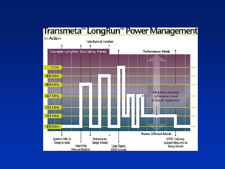
 Variable-supply Architectures • High-efficiency adjustable DC-DC converter • Adjustable synchronization – Variable-frequency clock generator [Chandrakasan 96] – Self-timed circuits [Nielsen 94] • Example: Power-pro architecture [Ishiara 98], Crusoe embedded processor [Transmeta 00] Prog ROM Dec Power Manager CPU Data RAM DC-DC & VCO Vdd CLK
") Basic problem formulation • Given a task, with known WCET and deadline d Vdd(S) – Find the optimal voltage for the processor that runs it WCET sl (minimize energy without violating d) Vmax d VT ST=(WCET+sl)/WCET 1 l ST is the “stretching factor” ST S
Basic problem formulation • Given a task, with known WCET and deadline d Vdd(S) – Find the optimal voltage for the processor that runs it WCET sl (minimize energy without violating d) Vmax d VT ST=(WCET+sl)/WCET 1 l ST is the “stretching factor” ST S
 resolution • Frequency interpolation Task Energy – Given a") Accounting for limited (f, Vdd) resolution • Frequency interpolation Task Energy – Given a task with N operations – Compute optimum (fideal, Vdd, ideal) – Find the two closest available frequencies The task executes all its N cycles at V 1: E = NEV 1 • f. L
Accounting for limited (f, Vdd) resolution • Frequency interpolation Task Energy – Given a task with N operations – Compute optimum (fideal, Vdd, ideal) – Find the two closest available frequencies The task executes all its N cycles at V 1: E = NEV 1 • f. L
 DVS l Many problems with RT DVS in practice n No task") Non-RT (interactive) DVS l Many problems with RT DVS in practice n No task characterization No C, no D n Dynamic task sets n Unknown dependencies n Not even a clear definition of task – l E. g. MP 3 play is a single application In most cases, RT DVS is simply not a realistic formulation
Non-RT (interactive) DVS l Many problems with RT DVS in practice n No task characterization No C, no D n Dynamic task sets n Unknown dependencies n Not even a clear definition of task – l E. g. MP 3 play is a single application In most cases, RT DVS is simply not a realistic formulation
 Non-RT DVS: design issues • When to take speed setting decisions – Slotted time (interval schedulers) vs. taskbased vs. event triggered • How to compute workload – Processor utilization is a good metric? • How to estimate performance constraints? • What speed is the right one?
![A basic approach [Grunwald 01] Experiments on PDA l Interval scheduler l PM decisions](https://present5.com/presentation/b7cfba95f9176dd0992ad8fc8d23a863/image-48.jpg "A basic approach [Grunwald 01] Experiments on PDA l Interval scheduler l PM decisions") A basic approach [Grunwald 01] Experiments on PDA l Interval scheduler l PM decisions at fixed time intervals l Predict utilization l Set frequency l
A basic approach [Grunwald 01] Experiments on PDA l Interval scheduler l PM decisions at fixed time intervals l Predict utilization l Set frequency l
 Details • Measure utilization U by looking at cycles spent in idle process during time quantum (usually 0 or 100%) – Weighted average AVGN: Wt=(NWt-1+Ut-1)/(N+1) – Sliding window average – PAST (only previous frame) • Adjust CLK speed to maximize utilization: – PEG (min-max), ONE, DOUBLE – With or without hysteresis Clock speed Speed setting decisions every RT clock interrupt (10 ms time quantum) – Overhead in execution time only 0. 6% CPU load • time
 AVS
AVS
 AVS II
 AVS
AVS
 AVS
AVS
 Modifying applications • Idea: two samples are buffered and their work loads are averaged – Averaged workload is then used as the effective workload to drive the power supply • A pingpong buffering scheme – Data samples In +2, In +3 are being buffered while In, In +1 are being processed.
 Impact of buffering
 if A > 0 then Flong(A) else Fshort(A) Compiler inserts") Compilers can help! A=foo() if A > 0 then Flong(A) else Fshort(A) Compiler inserts voltage switching points based on control/dataflow analysis CKPT A<=0 A>0 T=K/f f 2=50 MHz f 1=100 MHz
Compilers can help! A=foo() if A > 0 then Flong(A) else Fshort(A) Compiler inserts voltage switching points based on control/dataflow analysis CKPT A<=0 A>0 T=K/f f 2=50 MHz f 1=100 MHz
 Multi-Mode CT model with overhead • The tile operates in S states – Variable fclk and, optionally, variable Vdd (better!) – Delay and power overhead for state transitions • Power minimization t 1. Maximize slack 2. Chose best state considering transition overhead
 The origins: multiple sleep states Example: STRONGARM SA 1100 400 m. W • RUN: operational • IDLE: a sw routine may stop the CPU when not in use, while monitoring interrupts • SLEEP: Shutdown of on -chip activity RUN 10 us 90 us 160 ms 10 us 90 us IDLE SLEEP 50 m. W 160 u. W
 Low Power DRAMs • Conventional DRAMs refresh all rows with a fixed single time interval – read/write stalled while refreshing – refresh period -> tref – DRAM power = k * (#read/writes + #ref) • We have to worry about optimizing refresh operations
 – add a valid bit to each") Optimizing Refresh • Selective refresh architecture (SRA) – add a valid bit to each memory row, and only refresh rows with valid bit set – reduces refresh 5% to 80% • Variable refresh architecture (VRA) – data retention time of each cell is different – add a refresh period table and refresh counter to each row and refresh with the appropriate period to each row – reduces refresh about 75% [Ohsawa, 1995]
Optimizing Refresh • Selective refresh architecture (SRA) – add a valid bit to each memory row, and only refresh rows with valid bit set – reduces refresh 5% to 80% • Variable refresh architecture (VRA) – data retention time of each cell is different – add a refresh period table and refresh counter to each row and refresh with the appropriate period to each row – reduces refresh about 75% [Ohsawa, 1995]
 Cached DRAM • Integrates a cache on a DRAM chip that optimizes cost/performance/energy • Relies on the fact that SRAM accesses are faster then DRAM accesses • Different from traditional on-processor caches because of the width of transfer
 Banked DRAM Architecture CPU + Caches 0 N Bank N-1 2 N Bank 2 N-1 3 N 3 N-1 Bank 4 N-1
 DRAM Operating Modes 3. 75 n. J Active 2 cycles 30 cycles Standby Napping 0. 83 n. J 0. 32 n. J 9000 cycles Power-Down 0. 005 n. J
 • High bandwidth (>1. 5 GB/sec) • Each RDRAM module can") Rambus DRAM (RDRAM) • High bandwidth (>1. 5 GB/sec) • Each RDRAM module can be activated/deactivated independently • Read/write can occur only in the active mode • Three low-power operating modes: – Standby, Nap, Power-Down – In general, the lowest power modes have the longest operational latencies (e. g. , the relative power levels of power -down and standby states have a ratio of about 1: 100, and the relative access latencies to read data have a ratio of about 5000: 1) – Both high speed and low power operating modes serving the needs of both line-operated and portable products
Rambus DRAM (RDRAM) • High bandwidth (>1. 5 GB/sec) • Each RDRAM module can be activated/deactivated independently • Read/write can occur only in the active mode • Three low-power operating modes: – Standby, Nap, Power-Down – In general, the lowest power modes have the longest operational latencies (e. g. , the relative power levels of power -down and standby states have a ratio of about 1: 100, and the relative access latencies to read data have a ratio of about 5000: 1) – Both high speed and low power operating modes serving the needs of both line-operated and portable products
 Power Blocks disabled Mode Standby COL muxes disabled Napping COL and") Rambus DRAM (RDRAM) Power Blocks disabled Mode Standby COL muxes disabled Napping COL and ROW muxes disabled Power-Down COL and ROW muxes and clock synchronization disabled
Rambus DRAM (RDRAM) Power Blocks disabled Mode Standby COL muxes disabled Napping COL and ROW muxes disabled Power-Down COL and ROW muxes and clock synchronization disabled
 The opportunity Reduce power according to workloads device states shut down busy idle working power states wake up Tsd Tbs Tsd: shutdown delay Tbs: time before shutdown sleeping Twu working Tbw Twu: wakeup delay Tbw: time before wakeup Shutdown only during long idle time
? Predicting the future!") The challenge Is an idle period long enough for shutdown (Tbe)? Predicting the future!
The challenge Is an idle period long enough for shutdown (Tbe)? Predicting the future!
![Adaptive Stochastic Models Sliding Window (SW) [Chung DATE 99] B I ………. . .](https://present5.com/presentation/b7cfba95f9176dd0992ad8fc8d23a863/image-68.jpg "Adaptive Stochastic Models Sliding Window (SW) [Chung DATE 99] B I ………. . .") Adaptive Stochastic Models Sliding Window (SW) [Chung DATE 99] B I ………. . . B B I I B B B time Interpolating pre-computed optimization tables to determine power states using sliding windows to adapt for non-stationarity
Adaptive Stochastic Models Sliding Window (SW) [Chung DATE 99] B I ………. . . B B I I B B B time Interpolating pre-computed optimization tables to determine power states using sliding windows to adapt for non-stationarity
 Performance of predictors P : average power Nsd: number of shutdowns Nwd : wrong shutdowns (actually waste energy) [Yung D&T 2001]
 Can I do better than that? Improve workload information Application-aware DPM!
 OS-based DPM user requesters OS scheduler program DPM API power manager Interaction with scheduler device
 Interaction with OS • Concurrent processes – Created, executed, and terminated – Have different device utilization – Generate requests only when running (occupy CPU) • Power manager is notified when processes change state • Processes ask for “service levels” to the PM
 Can I do better than that? Application-level DPM Shaping the workload!
 Task Scheduling Rearrange task execution to cluster similar utilization and idle periods t 1 t 2 t 3 1 2 1 1 idle 1 2 1 T 1 2 2 3 time idle 2 3 3 2 3 idle T: time quantum
![Compilers can help! i = 1; while i <= N { read chunk[i] of](https://present5.com/presentation/b7cfba95f9176dd0992ad8fc8d23a863/image-75.jpg "Compilers can help! i = 1; while i <= N { read chunk[i] of") Compilers can help! i = 1; while i <= N { read chunk[i] of file; compute on chunk[i]; i = i+1; } Code transformation clusters disk accesses available = how_much_memory(); numchunks = available/sizeof(chunks); compute_time = appfunc(numchunks); i = 1; while i <= N { read chunk[i…i+numchunks] of file; next_R(compute_time); compute on chunk[i…i+numchunks]; i = i+numchunks; }
Compilers can help! i = 1; while i <= N { read chunk[i] of file; compute on chunk[i]; i = i+1; } Code transformation clusters disk accesses available = how_much_memory(); numchunks = available/sizeof(chunks); compute_time = appfunc(numchunks); i = 1; while i <= N { read chunk[i…i+numchunks] of file; next_R(compute_time); compute on chunk[i…i+numchunks]; i = i+numchunks; }
 CPU Disk CPU idle active Disk active") Impact on workload An Unmodified Application (UM) CPU Disk CPU idle active Disk active idle Transformed Application: Better clustering & opportunity for latency Elimination by early re-activation
Impact on workload An Unmodified Application (UM) CPU Disk CPU idle active Disk active idle Transformed Application: Better clustering & opportunity for latency Elimination by early re-activation
 Leakage Energy Management E 1, P 1 IALU 0 IALU 1 MULT FPALU BR LD/ST Apply run-time leakage control
 Compiler-Directed Leakage Mgmt. • Input vector control can benefit when El/Ed 1 / [ k – r - r (k-1) ] where k is the slack duration in cycles r is the leakage energy reduction “factor” E l = p Ed
 Multiple Tiles: the Tileboard model • System is viewed as a set of tiles – Tiles can be heterogeneous (e. g. CPU & Memory) – Modes can be different (e. g. no DVS for DRAMS) • Now, the problems gets really complicated
") Morphable memory system • Memory hierarchy can adapt to worload – Statically (compiler controlled) – Dynamically (OS controlled) – Sinergistically • Can be applied to multiple memory levels – Low levels: cache vs. scratchpad – High levels: DRAM shutdown PE B 1 B 2 B 3 L 1 B 2 L 2 B 1 B 2 L 3
Morphable memory system • Memory hierarchy can adapt to worload – Statically (compiler controlled) – Dynamically (OS controlled) – Sinergistically • Can be applied to multiple memory levels – Low levels: cache vs. scratchpad – High levels: DRAM shutdown PE B 1 B 2 B 3 L 1 B 2 L 2 B 1 B 2 L 3
 So. C Architecture evolution IO IO IO COPR NOC SOCBUS CPU MEM MEM NOC MEM • From single-master CPU to MPSo. C • From bus-based interconnect to No. C • Emphasize reuse, flexibility A distributed system on a single chip!
 Constant Variable Throughput/Latency Design Time Active Logic design (Dynamic) Trans") Power Design Space (Processor) Constant Variable Throughput/Latency Design Time Active Logic design (Dynamic) Trans sizing [C V 2 f] Sleep Mode Multiple VDD’s Standby (Leakage) [V Ioff] Run Time DFS Clock gating DVS DTM Stack effect Sleep trans Multiple VT’s Multi-VDD Multiple tox’s Variable VT Input control Variable VT
Power Design Space (Processor) Constant Variable Throughput/Latency Design Time Active Logic design (Dynamic) Trans sizing [C V 2 f] Sleep Mode Multiple VDD’s Standby (Leakage) [V Ioff] Run Time DFS Clock gating DVS DTM Stack effect Sleep trans Multiple VT’s Multi-VDD Multiple tox’s Variable VT Input control Variable VT
 SRAMs Active Partitioned caches (Dynamic) Way prediction [C V 2") Power Design Space (Memory) SRAMs Active Partitioned caches (Dynamic) Way prediction [C V 2 f] Filter caches Standby Higher VT’s (Leakage) Gated-GND or VDD [V Ioff] Drowsy caches e. DRAMS Mode control Gated-VDD
Power Design Space (Memory) SRAMs Active Partitioned caches (Dynamic) Way prediction [C V 2 f] Filter caches Standby Higher VT’s (Leakage) Gated-GND or VDD [V Ioff] Drowsy caches e. DRAMS Mode control Gated-VDD
 Shared Bus Crossbar DVS Signal encoding Active (Dynamic) [C V") Power Design Space (Interconnect) Shared Bus Crossbar DVS Signal encoding Active (Dynamic) [C V 2 f] Differential signaling Signal encoding Bus multiplexing Logic design Code compression Layout Error coding Standby (Leakage) [V Ioff] Drowsy buffers Variable VT No. C Gated-VDD DLS Routing alg’s Current vs. voltage mode Routing alg’s CV mode
Power Design Space (Interconnect) Shared Bus Crossbar DVS Signal encoding Active (Dynamic) [C V 2 f] Differential signaling Signal encoding Bus multiplexing Logic design Code compression Layout Error coding Standby (Leakage) [V Ioff] Drowsy buffers Variable VT No. C Gated-VDD DLS Routing alg’s Current vs. voltage mode Routing alg’s CV mode
 – Analysis step reveals low register") Power optimization • Compile-time control (no HW monitors) – Analysis step reveals low register pressure insert partial shutdown RF instruction – If non-critical FP operation scale down Vdd for the FPUs – If FPU soon needed pre-wakeup (hide latency) • Run-time control (requires HW probes) – Limit speculation if branch prediction inaccurate (partially disable IQ) – Disable execution units if unused • Sinergistic strategies are possible – Compiler “hints”, OS decides
Power optimization • Compile-time control (no HW monitors) – Analysis step reveals low register pressure insert partial shutdown RF instruction – If non-critical FP operation scale down Vdd for the FPUs – If FPU soon needed pre-wakeup (hide latency) • Run-time control (requires HW probes) – Limit speculation if branch prediction inaccurate (partially disable IQ) – Disable execution units if unused • Sinergistic strategies are possible – Compiler “hints”, OS decides
 Dynamically manageable CPU Integer IQ bpred voltage and frequency Fetch Memory fetch queue fetch decode IU rename dispatch LSQ Integer reg file L 2 Unified L 1 Dcache Cache voltage and frequency L 1 Icache voltage and frequency High-performance processor divided in many controllable tiles Floating Pt FPQ voltage and frequency FPU flt pt reg file
 Energy Savings and Performance Cost
 Highly controllable tiles • Multiple voltage distribution grids • Multiple clocks – No global reference • Multiple thresholds – Leakage control NOC • Dynamically adjustable – Clock frequencies – Device thresholds – Voltage supplies [IBM ICCAD 02] NOC Vdd 1 Vdd 2 Vdd 3
 Voltage island DPM • Decisions on speed, power supply, shutdown mode can be taken on a voltage-island basis – A local power manager controls mode of operations • Transition costs are reduced, but not nullified – Transitions have a penalty – Useless transitions should be avoided • Island granularity cannot be arbitrarily low – Design-time clustering – Accounting for inter-island communication overhead
 Centralized DPM • Single power manager for the entire SOC • Advantages – Global system knowledge – Similar to “traditional” DPM NO C • Disadvantages – Information collection bottleneck – Command distribution bottleneck – Policy complexity explosion Viable as a transition solution: not scalable NO C
 Distributed DPM • A power manager for each component • Advantages – Highly scalable – No communication overhead NO C • Disadvantages – Lacks of global information NO C – Poor workload knowledge – Doesn’t exploit high bandwidth on-chip communication channels Viable and scalable, but not very aggressive
 Message-passing DPM • Distributed PMs send messages on the NOC • Advantages – Scalable with the No. C – Complexity is tunable – Has global workload info NO C • Disadvantages – More hardware overhead than distributed – Added traffic (and power) for messages Viable and scalable, but not explored yet
 Many degrees of freedom. . . Putting it all together Infrastructure work!
 Busy/Idle process info Performance PM commands scheduling” suggestions”") Closed-loop control Power Workload System (plant) Busy/Idle process info Performance PM commands scheduling” suggestions” Power manager (controller) • Stabilizes the system • Reduces sensitivity to “modeling noise” • Challenge: high quality power/performance sampling
Closed-loop control Power Workload System (plant) Busy/Idle process info Performance PM commands scheduling” suggestions” Power manager (controller) • Stabilizes the system • Reduces sensitivity to “modeling noise” • Challenge: high quality power/performance sampling
 Conclusion • DPM is a rich research field – We have finally broken the ice: many techniques are showing promise – IC technology is coming this way • The reinassance? – We need infrastructure – We need convincing paths to market