b8b69475f2051199d6432b394bacba1a.ppt
- Количество слайдов: 60
 ELE 22 MIC Lectures 14 & 15 • RS 232 Line Drivers • Charge Pumps • Noise – Earth Loops, – Null Modems, Isolators, Modems • RS 485 Networking • Designing a microprocessor: – Chip Select Logic – Timing diagrams
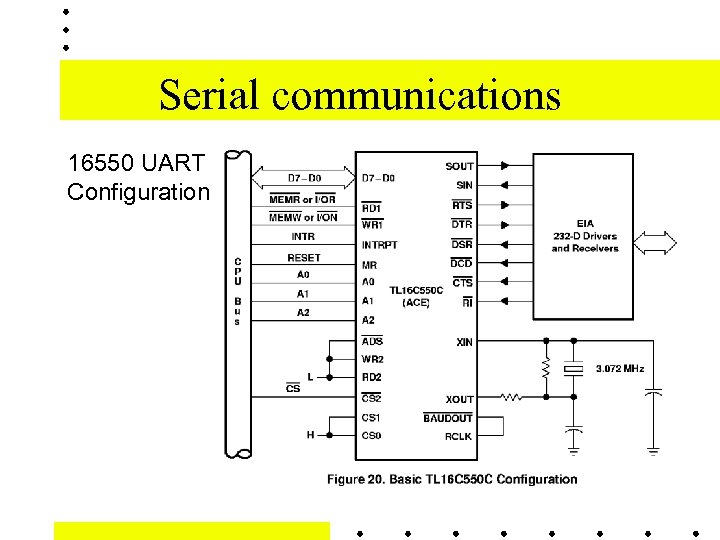 Serial communications 16550 UART Configuration
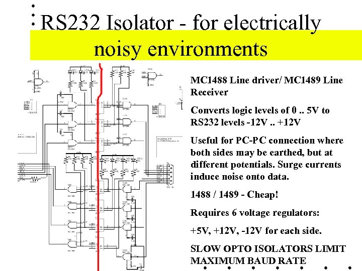 RS 232 Isolator - for electrically noisy environments MC 1488 Line driver/ MC 1489 Line Receiver Converts logic levels of 0. . 5 V to RS 232 levels -12 V. . +12 V Useful for PC-PC connection where both sides may be earthed, but at different potentials. Surge currents induce noise onto data. 1488 / 1489 - Cheap! Requires 6 voltage regulators: +5 V, +12 V, -12 V for each side. SLOW OPTO ISOLATORS LIMIT MAXIMUM BAUD RATE
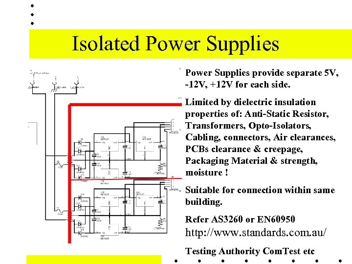 Isolated Power Supplies provide separate 5 V, -12 V, +12 V for each side. Limited by dielectric insulation properties of: Anti-Static Resistor, Transformers, Opto-Isolators, Cabling, connectors, Air clearances, PCBs clearance & creepage, Packaging Material & strength, moisture ! Suitable for connection within same building. Refer AS 3260 or EN 60950 http: //www. standards. com. au/ Testing Authority Com. Test etc
 MAX 232 • The MAX 232 contains two EIA 232 (RS 232) Transmitters & two Receivers in one package. • The MAX 232 has better noise immunity and zap and latch-up protection.
 MAX 232 • The MAX 232 contains both a Voltage Doubler and a Voltage Inverter • Voltage is Doubled via Charge Pump – A capacitor (C 1) is charged across the supply rails. – Then the charged capacitor is level shifted to the higher supply rail – The Charged capacitor transfers its charge into an output filter capacitor (C 2) – Process repeats at a very high rate pumping charge onto the output filter capacitor.
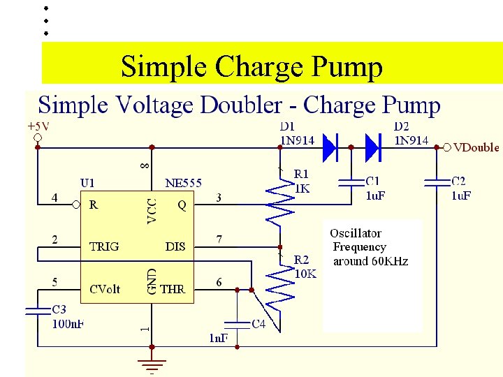 Simple Charge Pump
 Charge Pump • VDouble = (2 * 5 V) - (2 x 1 N 914 Vdrop) = 10 - 0. 8 V = 9. 2 V • This doubler shows the principle behind the concept. • In the MAX 232 the charge is transferred via FETs and so less voltage is lost. • A similar arrangement can be imagined for the voltage inverter.
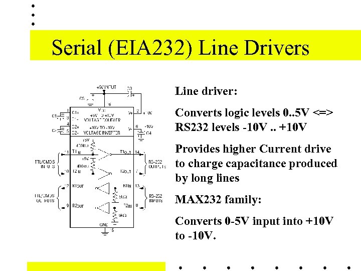 Serial (EIA 232) Line Drivers Line driver: Converts logic levels 0. . 5 V <=> RS 232 levels -10 V. . +10 V Provides higher Current drive to charge capacitance produced by long lines MAX 232 family: Converts 0 -5 V input into +10 V to -10 V.
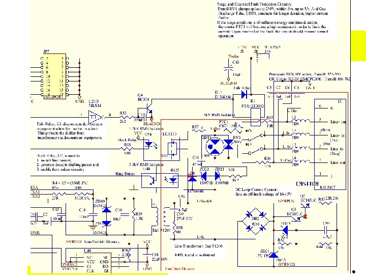
 Modem: Modulator Demodulator • For longer distances where different buildings are interconnected via telephone system wiring. • Leased Line Modems don’t require line voltage • PABX/PSTN lines require current limited line voltage • Distance - 10 kms - determined by cable losses & noise. • Phone Line connected Equipment requires ATick, C-Tick, & safety approvals
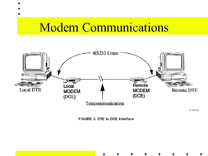 Modem Communications
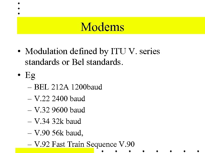 Modems • Modulation defined by ITU V. series standards or Bel standards. • Eg – BEL 212 A 1200 baud – V. 22 2400 baud – V. 32 9600 baud – V. 34 32 k baud – V. 90 56 k baud, – V. 92 Fast Train Sequence V. 90
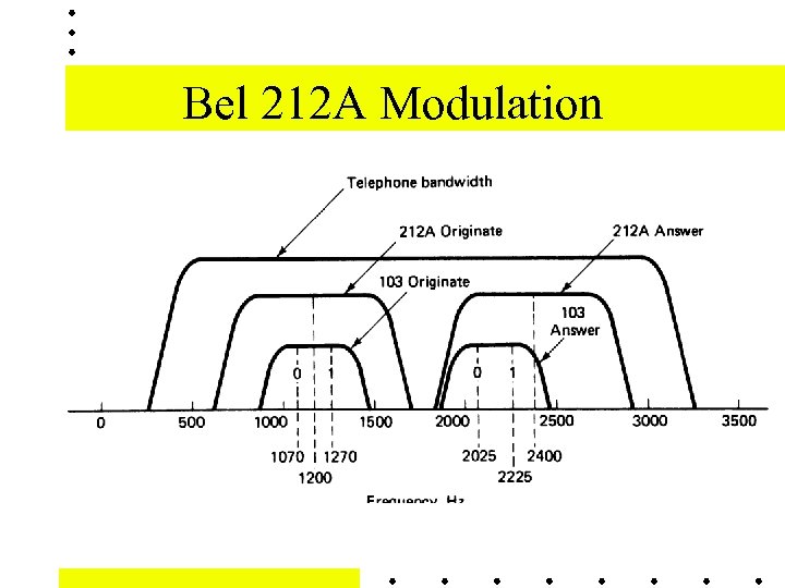 Bel 212 A Modulation
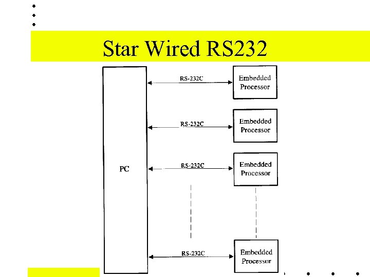 Star Wired RS 232
 2 C I Bus • Popular for peripheral interfacing • Two Wire (plus GND) bi-directional interface • 0 & 5 V logic levels • Suitable for short distance communication
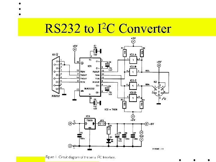 RS 232 to 2 C I Converter
 EIA/TIA/RS-485 (1) • Standard for differential multi-point data transmission • Popular over many years. • Up to 32 devices can communicate on a common RS 485 bus. • Can support multi-master configuration
 EIA RS-485 (2) • Line terminated at both ends into resistor equal to the characteristic impedance of cable (Typically 120 ohms). • Higher noise immunity than RS 232 - +/- 7 volts ground difference potential- rugged. • Tolerant of voltages -7 V. . +12 V and short circuits - In case of data packet collisions
 EIA RS-485 (3) • High speed - up to 10 Mbps (distance < 13 metres ) • Maximum cable run 1. 3 km @ 100 kbps. • Bus uses 2 -wire shielded cable. • Cheaper than RS 232 star-wiring • Trade-off speed vs power consumption of line driver
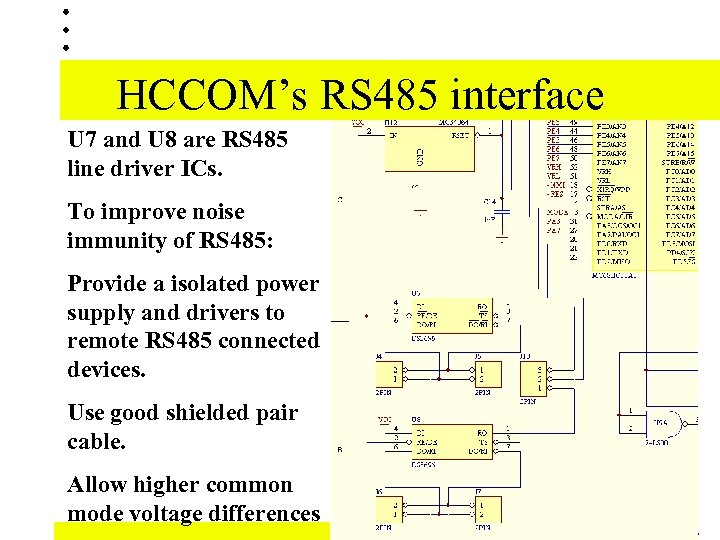 HCCOM’s RS 485 interface U 7 and U 8 are RS 485 line driver ICs. To improve noise immunity of RS 485: Provide a isolated power supply and drivers to remote RS 485 connected devices. Use good shielded pair cable. Allow higher common mode voltage differences
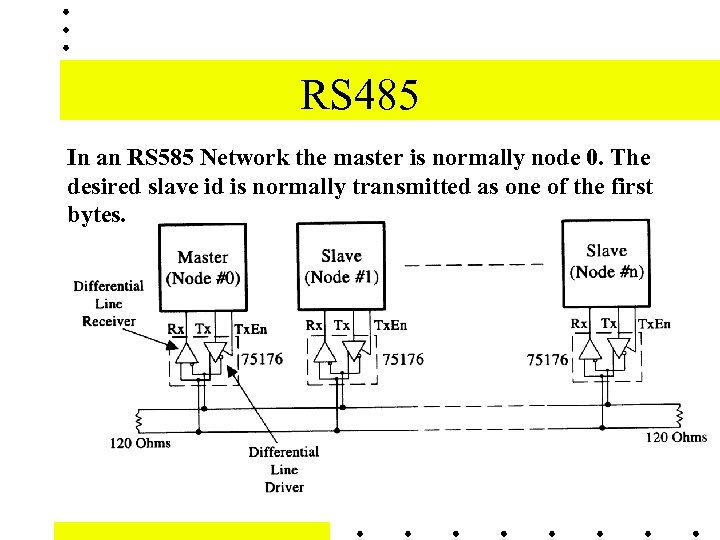 RS 485 In an RS 585 Network the master is normally node 0. The desired slave id is normally transmitted as one of the first bytes.
 RS 485 After sending its data the Master disables its drivers and waits for the Slave’s response. All receivers must listen to the traffic to determine what is being sent to which master/slave.
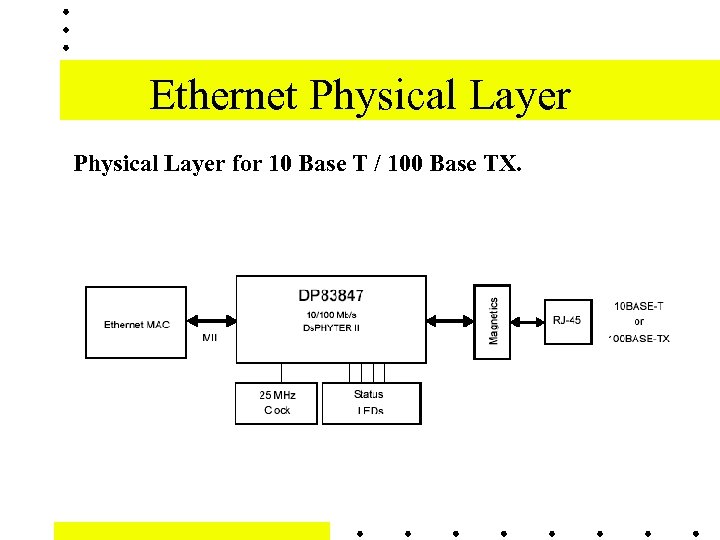 Ethernet Physical Layer for 10 Base T / 100 Base TX.
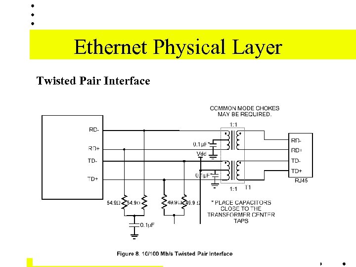 Ethernet Physical Layer Twisted Pair Interface
 Designing a 68 HC 11 based computer • Memory space considerations • We are going to outline a step-by-step procedure, using a practical example, for the design of a 68 HC 11 based computer. • We will be focusing on memory space considerations only in this lecture. So, the computer we will be designing may or may not work.
 Designing a 68 HC 11 based computer • This is because we have omitted the crucial timing considerations which is the topic for the next lecture. • It is only when both memory space interface and signal timing considerations are correctly taken into account in our design then we shall have some chance of getting a working computer system.
 Designing a 68 HC 11 based computer • The company you are working for is building a "radio teletype " for use as a message receiver at Mawson Base in Antarctica. • Digital status messages are received from remote weather stations. The incoming radio telemetry is decoded into ASCII by the radio receiver unit which then passes the data over a serial link to your system.
 Designing a 68 HC 11 based computer • Your system takes the ASCII codes received serially and asses them to a parallel printer. You have been given the task of writing the software that will control the system. • The interface to the printer consists of 8 data lines, one active-low BUSY line and one active-low STROBE.
 Designing a 68 HC 11 based computer • Operation of the printerface works as follows. The processor checks the status of the BUSY input line from the printer and waits until it is high (Printer not-busy). • The processor then places data on the printer's data lines and sends the STROBE output line low, then returns it high. This tells the Printer that new data is available for it.
 Designing a 68 HC 11 based computer • The radio receiver sends serial data to your system at 1200 bps, with 8 data bus, one stop bit and no parity bit. • The PIA lies at addresses $6000 to $6003 and the ACIA lies at addresses $7000 and $7001 in your memory space. • The ACIA has a serial clock running at 19. 2 k. Hz
 Designing a 68 HC 11 based computer • 1. Write initialisation routines to configure the ACIA appropriately. It is desirable to have the ACIA generate an interrupt when new data is received. • 2. Write intialisation routines to configure port B of the PIA as the data lines for the printer and bit 0 of port A as the BUSY line.
 Designing a 68 HC 11 based computer • In this system. We only want an interrupt generated when the ACIA receives data. so interrupts should be disabled on the PIA. The status of the BUSY line should be checked under software control, but the STROBE# may be generated using one of the PIA s output control lines. The STROBE# line should go low when data is written to port B.
 Designing a 68 HC 11 based computer • 3. Write an Interrupt Service Routine (ISR) that will read data from the ACIA when a character is received and send this to to the printer via the PIA. Your ISR should read data from the ACIA, check the status of the printer by examining bit 0 of PIA port A) and then send the data by storing it to port B of the PIA.
 Design Specification (1) • Always start with a few questions, like: • 1. – What is it comprised of ? – What is it for ? • Usually the answers are provided by the design specifications. – Here, a 68 HC 11 is the brain of the system. We also have a MC 6821 PIA and a MC 6850 ACIA for handling the system I/O.
 Design Specification (2) • 2. What does the system do ? – Receive data with the ACIA and Print data with the PIA on a printer. • 3. How do we attach the PIA and the ACIA to the 68 HC 11 ? – Available alternatives : • Port ? • Memory mapped ?
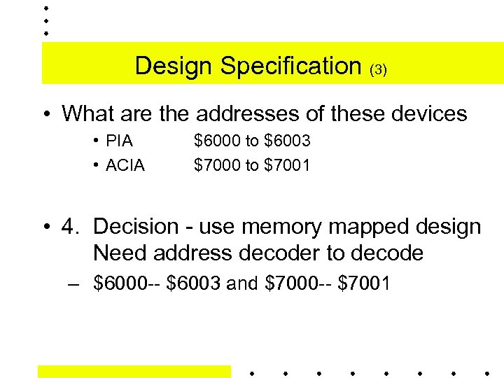 Design Specification (3) • What are the addresses of these devices • PIA • ACIA $6000 to $6003 $7000 to $7001 • 4. Decision - use memory mapped design Need address decoder to decode – $6000 -- $6003 and $7000 -- $7001
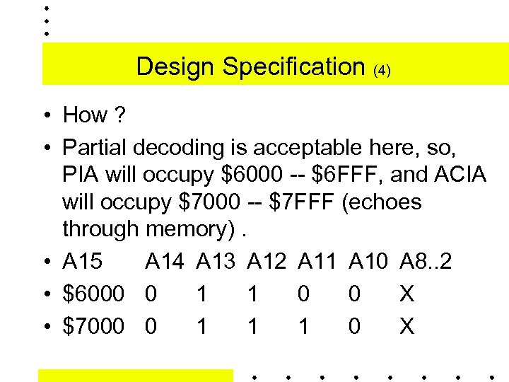 Design Specification (4) • How ? • Partial decoding is acceptable here, so, PIA will occupy $6000 -- $6 FFF, and ACIA will occupy $7000 -- $7 FFF (echoes through memory). • A 15 A 14 A 13 A 12 A 11 A 10 A 8. . 2 • $6000 0 1 1 0 0 X • $7000 0 1 1 1 0 X
 Design Specification (5) • Assuming the chip-select (CS) lines for both the PIA and the ACIA are active low, we can use the following address decoder: • 5. Whenever an external device is attached to the 68 HC 11, we need to initialise it.
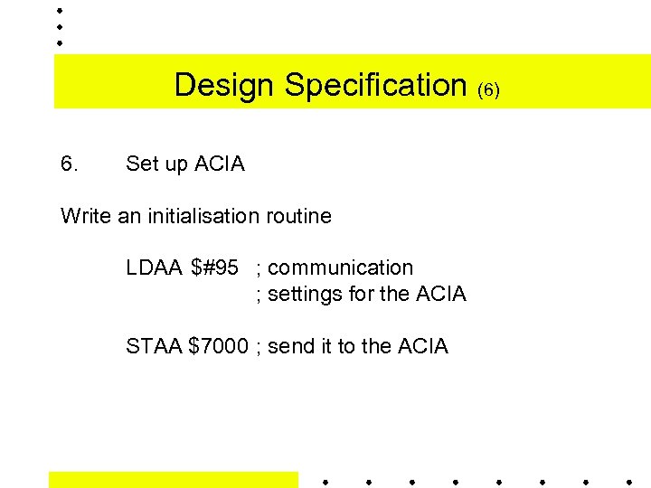 Design Specification (6) 6. Set up ACIA Write an initialisation routine LDAA $#95 ; communication ; settings for the ACIA STAA $7000 ; send it to the ACIA
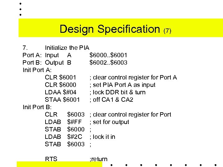 Design Specification (7) 7. Initialize the PIA Port A: Input A $6000. . $6001 Port B: Output B $6002. . $6003 Init Port A: CLR $6001 ; clear control register for Port A CLR $6000 ; set PIA Port A as input LDAA $#04 ; lock DDR bit & turn STAA $6001 ; off CA 1 & CA 2 Init Port B: CLR $6003 ; clear control register for Port LDAB $#FF ; set for output STAB $6000 ; LDAB $#2 C ; lock it in STAB $6003 ; RTS ; return
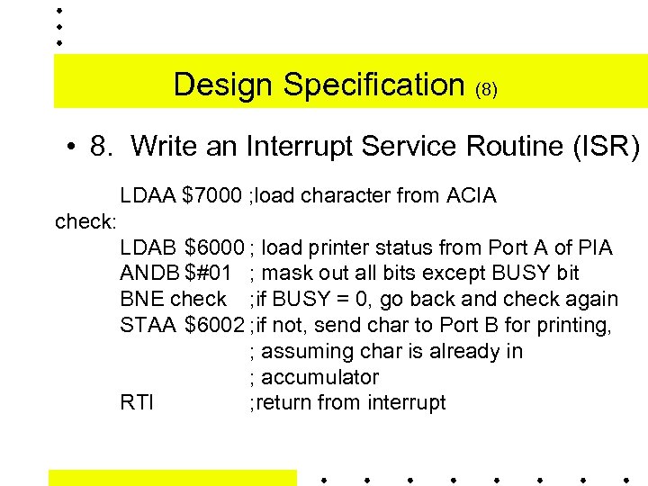 Design Specification (8) • 8. Write an Interrupt Service Routine (ISR) LDAA $7000 ; load character from ACIA check: LDAB $6000 ; load printer status from Port A of PIA ANDB $#01 ; mask out all bits except BUSY bit BNE check ; if BUSY = 0, go back and check again STAA $6002 ; if not, send char to Port B for printing, ; assuming char is already in ; accumulator RTI ; return from interrupt
 Design Specification (9) • 9. Environmental Considerations: – Air Conditioned ? – Inside / Outside? – Environmental extremes ? • • Temperature / Sunlight Humidity / Condensation - Drain Holes Iceing / Soot / Smoke Vibration / Stress relief
 Analog to Digital Converter • Analog to Digital Converter section of 68 HC 11 • Requires 32 E-clock cycles to complete a conversion • 8 -bit successive approximation converter. • Uses Charge re-distribution for manufacturability reasons. • As it is based upon capacitance it automatically includes Sample & Hold functionality
 Analog to Digital Converter • Analog switches are used to provide ADC internal capacitor switching and input multiplexor selection switching. • Uses internal charge pump -> 7 to 8 V – Provides high gate voltages to operate analog switches - guarantees low impedance. – must be enabled (disabled at reset) – A/D Power Up (ADPU) control bit – after starting charge pump, must delay 100 us before
 Analog to Digital Converter • Uses clock sources - must be selected • Four channels are converted in sequence with the results provided in registers
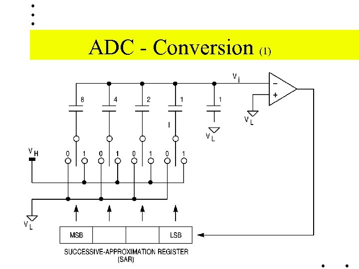
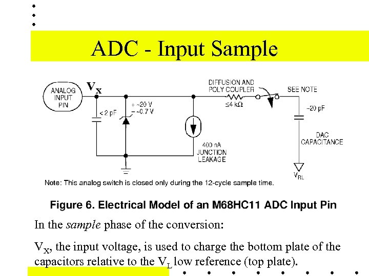 ADC - Input Sample VX In the sample phase of the conversion: VX, the input voltage, is used to charge the bottom plate of the capacitors relative to the VL low reference (top plate).
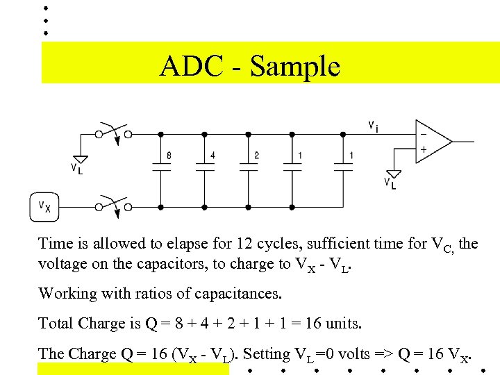 ADC - Sample Time is allowed to elapse for 12 cycles, sufficient time for VC, the voltage on the capacitors, to charge to VX - VL. Working with ratios of capacitances. Total Charge is Q = 8 + 4 + 2 + 1 = 16 units. The Charge Q = 16 (VX - VL). Setting VL =0 volts => Q = 16 VX.
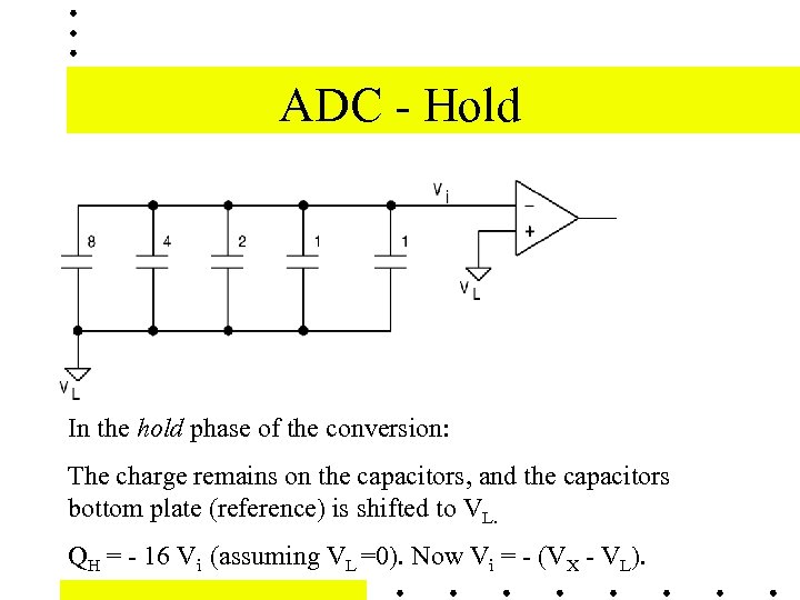 ADC - Hold In the hold phase of the conversion: The charge remains on the capacitors, and the capacitors bottom plate (reference) is shifted to VL. QH = - 16 Vi (assuming VL =0). Now Vi = - (VX - VL).
 ADC - Conversion (1)
 ADC - Conversion (2) In the Successive Approximation phase of the conversion: The voltage on the capacitors, is re-distributed between the 1 unit capacitor, and the VH reference voltage. The ratio of capacitance determines Vi = (VH/VL) CSEL/C 1. The resulting comparator input voltage is set reflects the input Resistive losses and timing are ignored to simplify analysis.
 ADC - Conversion (3) Starting with the 8 unit capacitor (MSB), it is switched VH. The charge is Q = 8 (VH - Vi) + 8 (VL - Vi). Q = 8 VH - 16 Vi assuming Vi = 0. The ratio of capacitance determines Vi = (VH/VL) CSAR/C 1. The resulting comparator input voltage is set reflects the input ratio. If the VX < 8/16 (VH - VL) then Vi > VL and the comparator will output a 1. C 8 is set to VH, and a 1 is saved in the MSB of the Successive Approximation register (SAR). Conversely if VX > 8/16 (VH - VL) then the comparator will output a 0. C 8 is set to VL, And a 0 is saved in the MSB of the Successive Approximation register.
 ADC - Conversion (4) Next the 4 unit capacitor (MSB), the capacitor is switched VH. The resulting comparator input voltage is set reflects the input ratio. And the SAR will save the value of the next most significant bit. The ADC continues through the rest of the bits until all capacitors have been set and the SAR holds the value of the conversion. Upon conversion completion: VX = (VH - VL) x (SAR / 256)
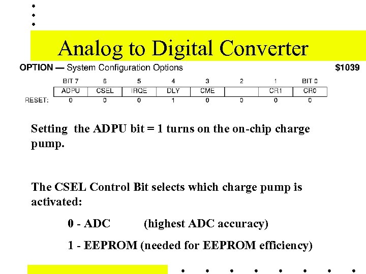 Analog to Digital Converter Setting the ADPU bit = 1 turns on the on-chip charge pump. The CSEL Control Bit selects which charge pump is activated: 0 - ADC (highest ADC accuracy) 1 - EEPROM (needed for EEPROM efficiency)
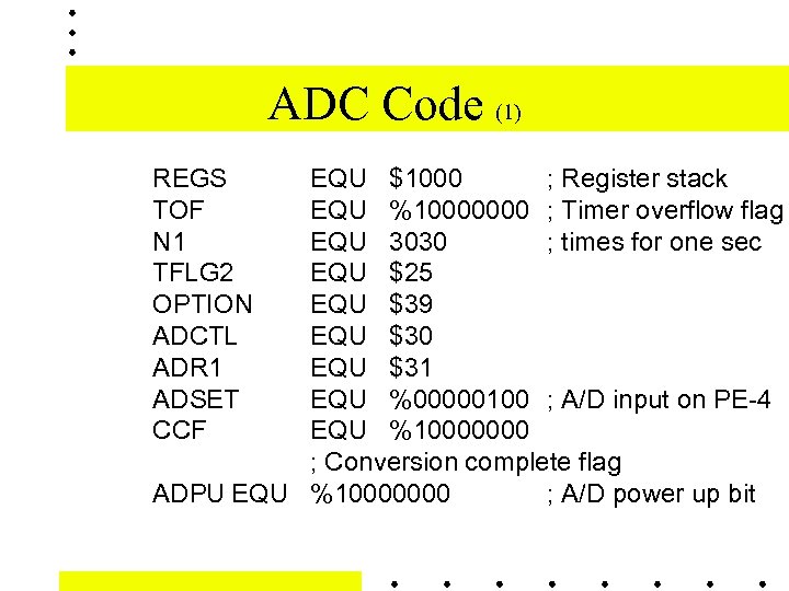 ADC Code (1) REGS TOF N 1 TFLG 2 OPTION ADCTL ADR 1 ADSET CCF EQU $1000 ; Register stack EQU %10000000 ; Timer overflow flag EQU 3030 ; times for one sec EQU $25 EQU $39 EQU $30 EQU $31 EQU %00000100 ; A/D input on PE-4 EQU %10000000 ; Conversion complete flag ADPU EQU %10000000 ; A/D power up bit
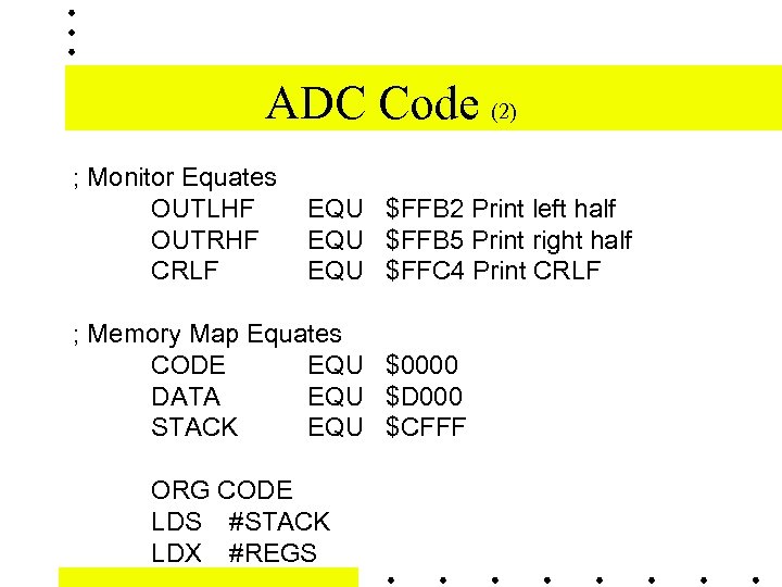 ADC Code (2) ; Monitor Equates OUTLHF OUTRHF CRLF EQU $FFB 2 Print left half EQU $FFB 5 Print right half EQU $FFC 4 Print CRLF ; Memory Map Equates CODE EQU $0000 DATA EQU $D 000 STACK EQU $CFFF ORG CODE LDS #STACK LDX #REGS
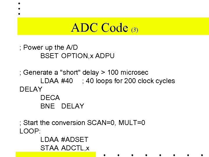 ADC Code (3) ; Power up the A/D BSET OPTION, x ADPU ; Generate a "short" delay > 100 microsec LDAA #40 ; 40 loops for 200 clock cycles DELAY DECA BNE DELAY ; Start the conversion SCAN=0, MULT=0 LOOP: LDAA #ADSET STAA ADCTL, x
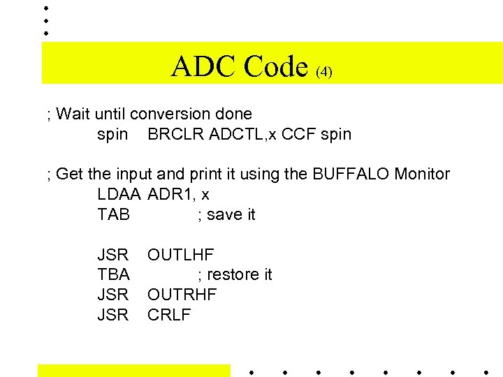 ADC Code (4) ; Wait until conversion done spin BRCLR ADCTL, x CCF spin ; Get the input and print it using the BUFFALO Monitor LDAA ADR 1, x TAB ; save it JSR TBA JSR OUTLHF ; restore it OUTRHF CRLF
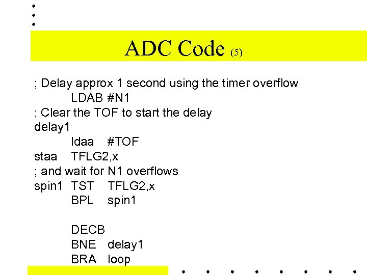 ADC Code (5) ; Delay approx 1 second using the timer overflow LDAB #N 1 ; Clear the TOF to start the delay 1 ldaa #TOF staa TFLG 2, x ; and wait for N 1 overflows spin 1 TST TFLG 2, x BPL spin 1 DECB BNE delay 1 BRA loop
 Acknowledgments • RS 485 diagrams from Embedded Systems Building Blocks - Complete Ready to Use Modules in C - Jean Labrosse, CMP Books, ISBN 087930 -604 -1. – For a complete ROMable micro-kernel see “Micro. C/OS-II The Real-Time Kernel” by Jean Labrosse, CMP Books, ISBN 0 -87930 -543 -6 http: //ucosii. com/ – Also discussed in Embedded Systems Programming Magazine. http: //www. embedded. com/mag. htm • Modulation Frequency Diagram – “Interfacing Sensors to the IBM PC”, Willis Tompkins/John Webster • I 2 C Interface to RS 232 (010045) – Elektor Electronics magazine, July/August 2001 Ingo Gerlach • National Semiconductor device data sheets & application notes: – DP 83847 - DP 83847. PDF – AN 979 The practical Limits of RS 485,


