d6c4abd72129207d69b7b6e23c9387eb.ppt
- Количество слайдов: 51
 Efficient Asynchronous Protocol Converters for Two-Phase Delay. Insensitive Global Communication Amitava Mitra Intel Corp. , Bangalore, India William F. Mc. Laughlin Columbia University, Electrical Engineering Steven M. Nowick Columbia University, Computer Science
 Outline ã Motivation and Contribution l System-on-Chip: Concepts and Trends l Asynchronous Signaling Styles l Target Asynchronous SOC Architecture l Contribution ã Proposed System Architecture ã Experimental Results ã Extensions: Other Signaling Styles ã Conclusions and Future Work 2
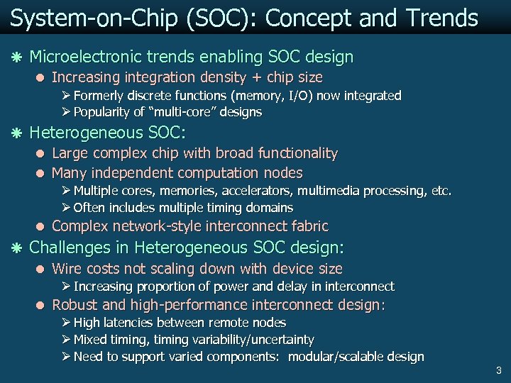 System-on-Chip (SOC): Concept and Trends ã Microelectronic trends enabling SOC design l Increasing integration density + chip size Ø Formerly discrete functions (memory, I/O) now integrated Ø Popularity of “multi-core” designs ã Heterogeneous SOC: l Large complex chip with broad functionality l Many independent computation nodes Ø Multiple cores, memories, accelerators, multimedia processing, etc. Ø Often includes multiple timing domains l Complex network-style interconnect fabric ã Challenges in Heterogeneous SOC design: l Wire costs not scaling down with device size Ø Increasing proportion of power and delay in interconnect l Robust and high-performance interconnect design: Ø High latencies between remote nodes Ø Mixed timing, timing variability/uncertainty Ø Need to support varied components: modular/scalable design 3
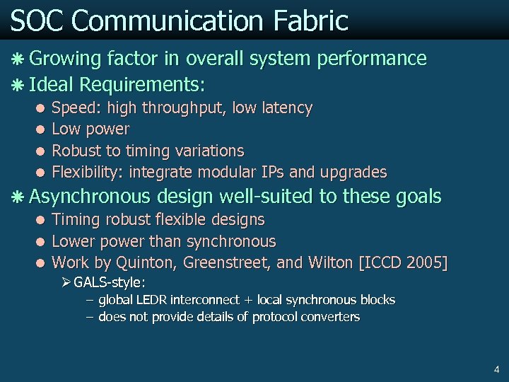 SOC Communication Fabric ã Growing factor in overall system performance ã Ideal Requirements: l Speed: high throughput, low latency l Low power l Robust to timing variations l Flexibility: integrate modular IPs and upgrades ã Asynchronous design well-suited to these goals l Timing robust flexible designs l Lower power than synchronous l Work by Quinton, Greenstreet, and Wilton [ICCD 2005] Ø GALS-style: – global LEDR interconnect + local synchronous blocks – does not provide details of protocol converters 4
 Asynchronous for SOC Communication ã Advantages of asynchronous global communication l Delay-insensitive (DI) encoding Ø Removes timing constraints on global routing l No clock signals to route across chip Ø Significant power advantage l Can support both async + sync computation Ø Delay-insensitive async logic combats growing variability concerns Ø GALS style: Globally-Asynchronous Locally-Synchronous ã Several popular async signaling protocols l Dual rail four-phase, LEDR, 1 -of-4, bundled data, others l No single protocol ideal for both logic and communication 5
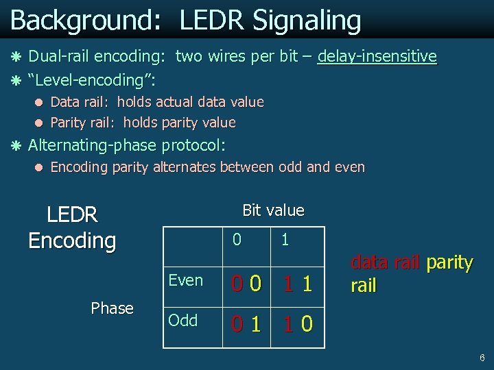 Background: LEDR Signaling ã Dual-rail encoding: two wires per bit – delay-insensitive ã “Level-encoding”: l Data rail: holds actual data value l Parity rail: holds parity value ã Alternating-phase protocol: l Encoding parity alternates between odd and even Bit value LEDR Encoding 0 1 Even Phase 00 11 Odd data rail parity rail 01 10 6
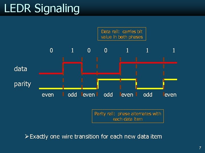 LEDR Signaling Data rail: carries bit value in both phases 0 1 0 0 1 1 even odd 1 data parity even odd even Parity rail: phase alternates with each data item Ø Exactly one wire transition for each new data item 7
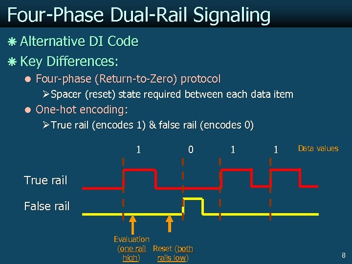 Four-Phase Dual-Rail Signaling ã Alternative DI Code ã Key Differences: l Four-phase (Return-to-Zero) protocol Ø Spacer (reset) state required between each data item l One-hot encoding: Ø True rail (encodes 1) & false rail (encodes 0) 1 0 1 1 Data values True rail False rail Evaluation (one rail Reset (both high) rails low) 8
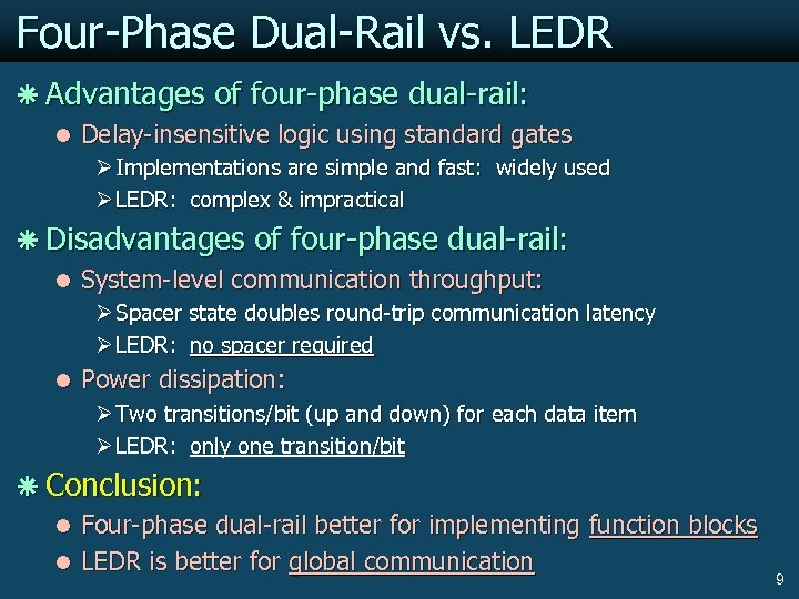 Four-Phase Dual-Rail vs. LEDR ã Advantages of four-phase dual-rail: l Delay-insensitive logic using standard gates Ø Implementations are simple and fast: widely used Ø LEDR: complex & impractical ã Disadvantages of four-phase dual-rail: l System-level communication throughput: Ø Spacer state doubles round-trip communication latency Ø LEDR: no spacer required l Power dissipation: Ø Two transitions/bit (up and down) for each data item Ø LEDR: only one transition/bit ã Conclusion: l Four-phase dual-rail better for implementing function blocks l LEDR is better for global communication 9
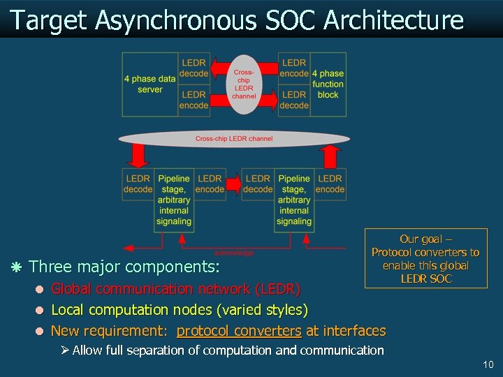 Target Asynchronous SOC Architecture Our goal – Protocol converters to enable this global LEDR SOC ã Three major components: l Global communication network (LEDR) l Local computation nodes (varied styles) l New requirement: protocol converters at interfaces Ø Allow full separation of computation and communication 10
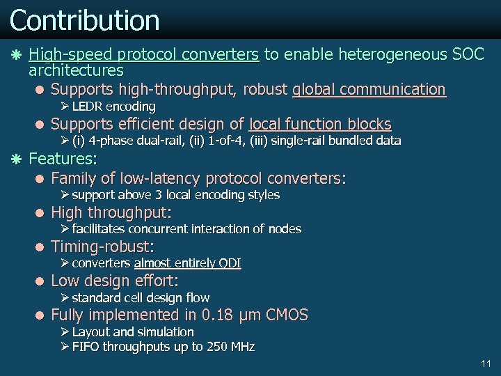 Contribution ã High-speed protocol converters to enable heterogeneous SOC architectures l Supports high-throughput, robust global communication Ø LEDR encoding l Supports efficient design of local function blocks Ø (i) 4 -phase dual-rail, (ii) 1 -of-4, (iii) single-rail bundled data ã Features: l Family of low-latency protocol converters: Ø support above 3 local encoding styles l High throughput: Ø facilitates concurrent interaction of nodes l Timing-robust: Ø converters almost entirely QDI l Low design effort: Ø standard cell design flow l Fully implemented in 0. 18 μm CMOS Ø Layout and simulation Ø FIFO throughputs up to 250 MHz 11
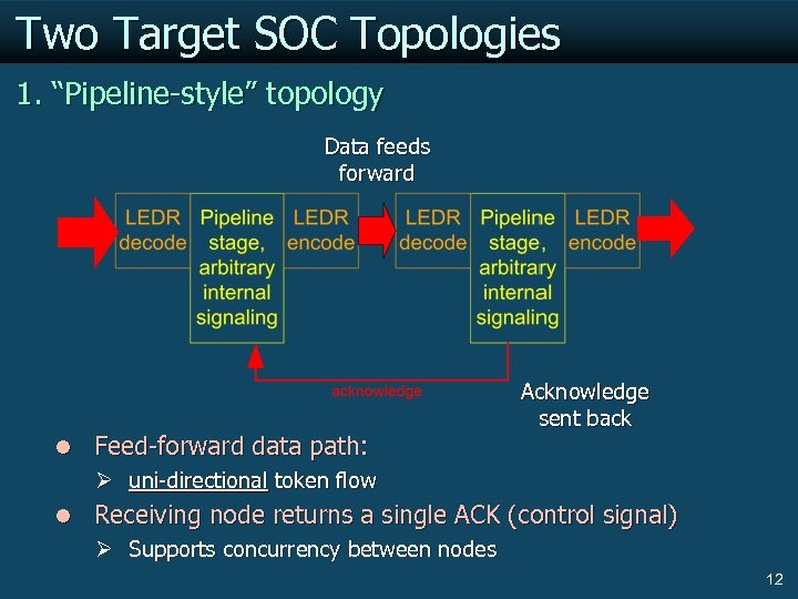 Two Target SOC Topologies 1. “Pipeline-style” topology Data feeds forward l Feed-forward data path: Ø uni-directional token flow Acknowledge sent back l Receiving node returns a single ACK (control signal) Ø Supports concurrency between nodes 12
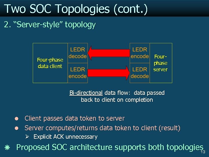 Two SOC Topologies (cont. ) 2. “Server-style” topology Fourphase server Four-phase data client Bi-directional data flow: data passed back to client on completion l Client passes data token to server l Server computes/returns data token to client (result) Ø Explicit ACK unnecessary ã Proposed SOC architecture supports both topologies 13
 Outline ã Motivation and Contribution ã Proposed System Architecture l Architecture Overview l System Simulation l Detailed Hardware Implementation l Timing Analysis ã Experimental Results ã Extensions: Other Signaling Styles ã Conclusions and Future Work 14
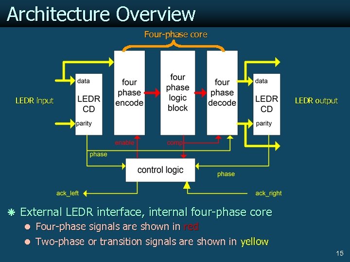 Architecture Overview Four-phase core LEDR input LEDR output ã External LEDR interface, internal four-phase core l Four-phase signals are shown in red l Two-phase or transition signals are shown in yellow 15
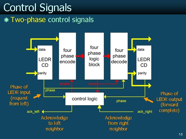 Control Signals ã Two-phase control signals Phase of LEDR input (request from left) Phase of LEDR output (forward complete) Acknowledge to left neighbor Acknowledge from right neighbor 16
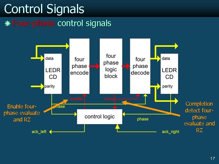 Control Signals ã Four-phase control signals Enable fourphase evaluate and RZ Completion detect fourphase evaluate and RZ 17
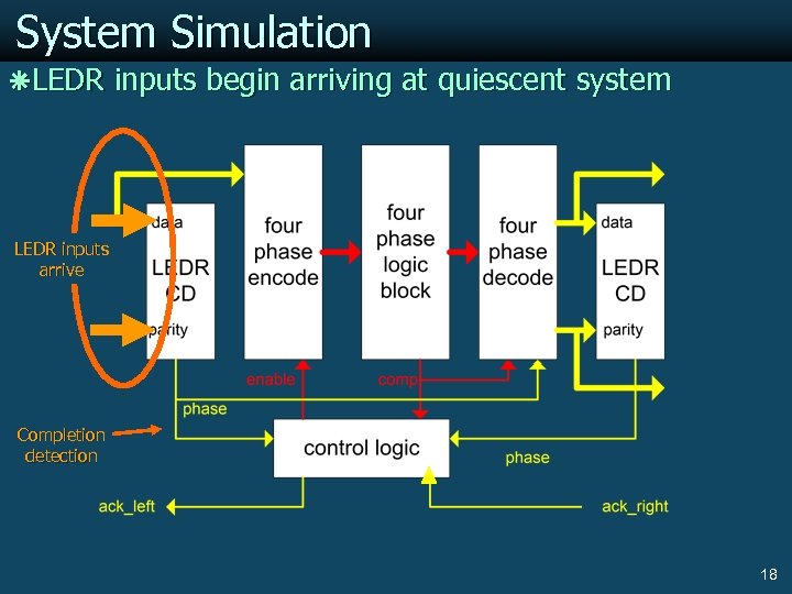 System Simulation ãLEDR inputs begin arriving at quiescent system LEDR inputs arrive Completion detection 18
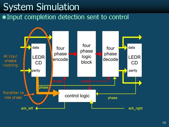 System Simulation ãInput completion detection sent to control All input phases matching Transition to new phase 19
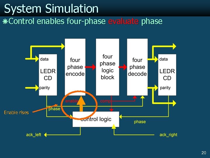 System Simulation ãControl enables four-phase evaluate phase Enable rises 20
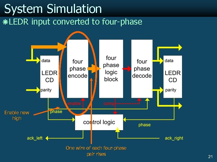 System Simulation ãLEDR input converted to four-phase Enable now high One wire of each four-phase pair rises 21
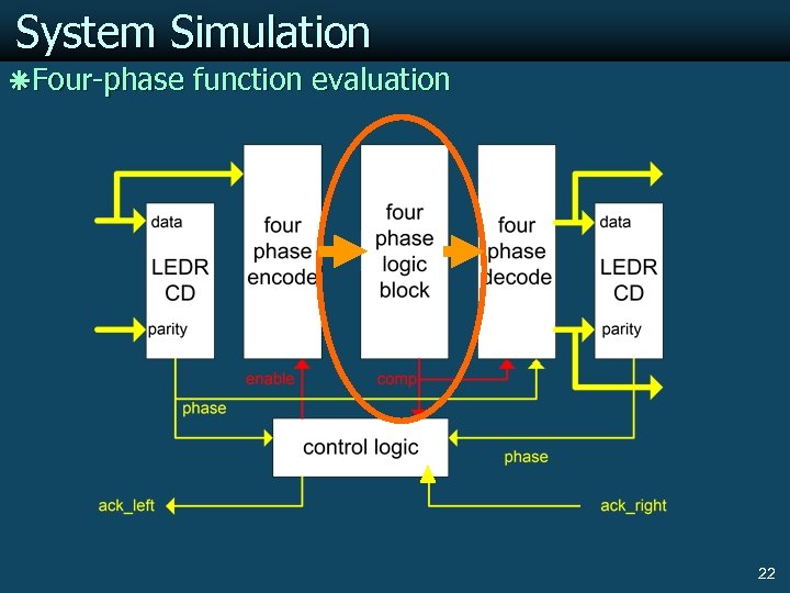 System Simulation ãFour-phase function evaluation 22
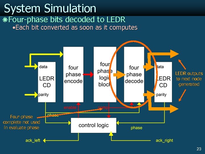 System Simulation ãFour-phase bits decoded to LEDR Each bit converted as soon as it computes LEDR outputs to next node generated Four-phase complete not used in evaluate phase 23
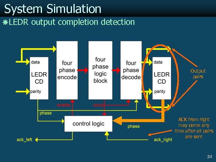 System Simulation ãLEDR output completion detection Output pairs ACK from right may come any time after all pairs are sent 24
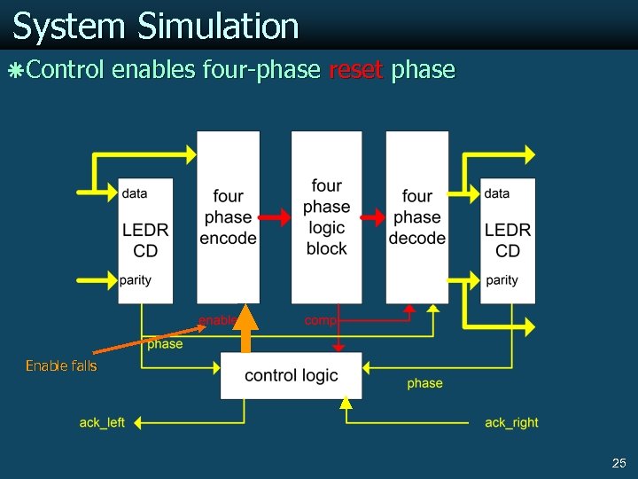 System Simulation ãControl enables four-phase reset phase Enable falls 25
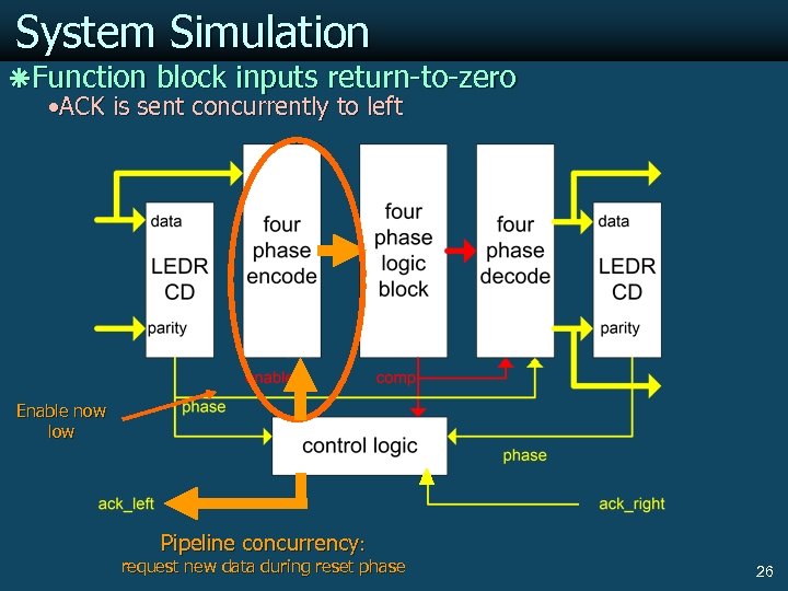 System Simulation ãFunction block inputs return-to-zero ACK is sent concurrently to left Enable now low Pipeline concurrency: request new data during reset phase 26
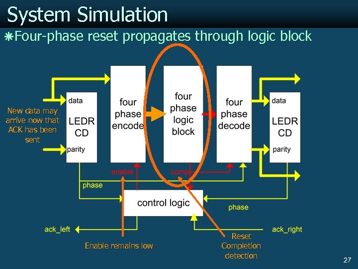 System Simulation ãFour-phase reset propagates through logic block New data may arrive now that ACK has been sent Enable remains low Reset Completion detection 27
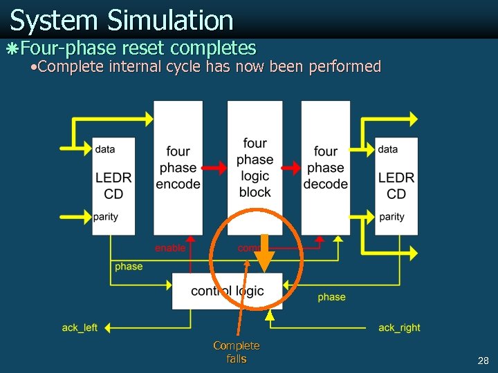 System Simulation ãFour-phase reset completes Complete internal cycle has now been performed Complete falls 28
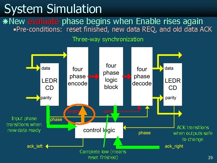 System Simulation ãNew evaluate phase begins when Enable rises again Pre-conditions: reset finished, new data REQ, and old data ACK Three-way synchronization Input phase transitions when new data ready ACK transitions when outputs safe to change Complete low (means reset finished) 29
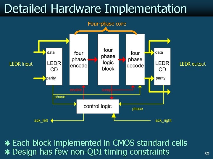 Detailed Hardware Implementation Four-phase core LEDR input LEDR output ã Each block implemented in CMOS standard cells ã Design has few non-QDI timing constraints 30
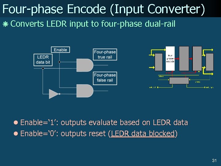 Four-phase Encode (Input Converter) ã Converts LEDR input to four-phase dual-rail l Enable=‘ 1’: outputs evaluate based on LEDR data l Enable=‘ 0’: outputs reset (LEDR data blocked) 31
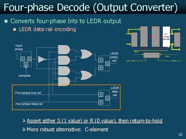 Four-phase Decode (Output Converter) ã Converts four-phase bits to LEDR output l LEDR data rail encoding Ø Assert either S (1 value) or R (0 value), then return-to-hold Ø More robust alternative: C-element 32
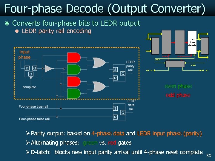 Four-phase Decode (Output Converter) ã Converts four-phase bits to LEDR output l LEDR parity rail encoding even phase odd phase Ø Parity output: based on 4 -phase data and LEDR input phase (parity) Ø Alternating phases: green vs. red gates Ø D-latch: blocks new input parity arrival until 4 -phase reset complete 33
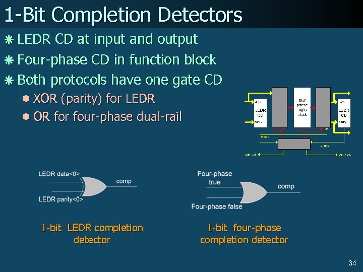 1 -Bit Completion Detectors ã LEDR CD at input and output ã Four-phase CD in function block ã Both protocols have one gate CD l XOR (parity) for LEDR l OR for four-phase dual-rail 1 -bit LEDR completion detector 1 -bit four-phase completion detector 34
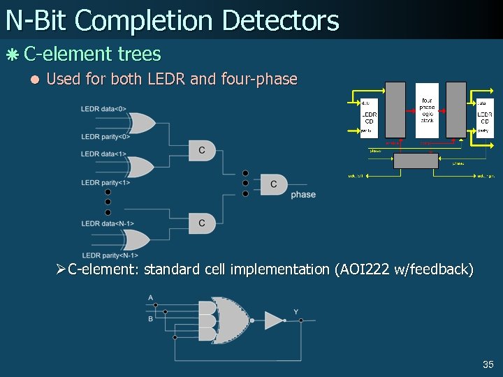 N-Bit Completion Detectors ã C-element trees l Used for both LEDR and four-phase Ø C-element: standard cell implementation (AOI 222 w/feedback) 35
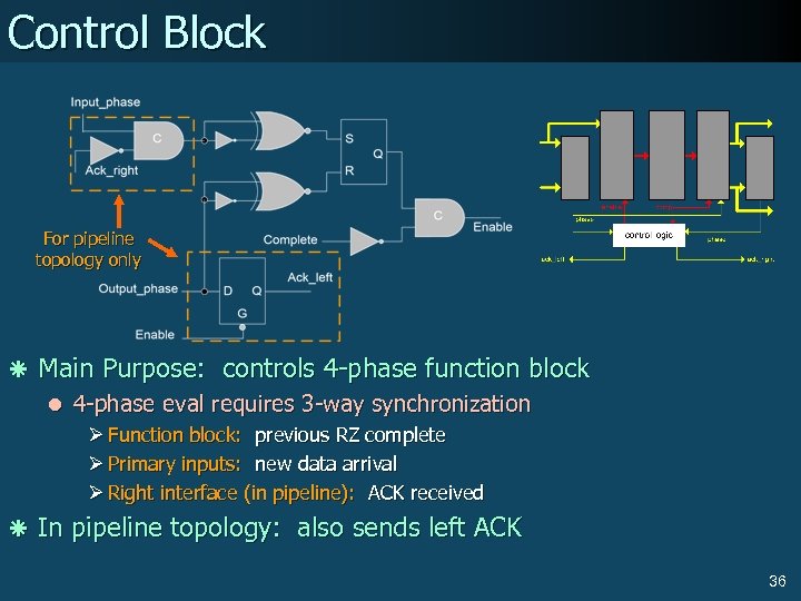 Control Block For pipeline topology only ã Main Purpose: controls 4 -phase function block l 4 -phase eval requires 3 -way synchronization Ø Function block: previous RZ complete Ø Primary inputs: new data arrival Ø Right interface (in pipeline): ACK received ã In pipeline topology: also sends left ACK 36
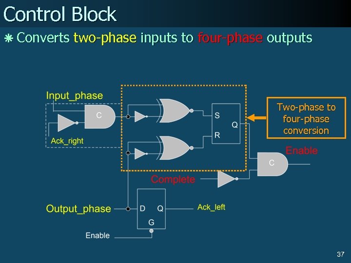 Control Block ã Converts two-phase inputs to four-phase outputs Two-phase to four-phase conversion 37
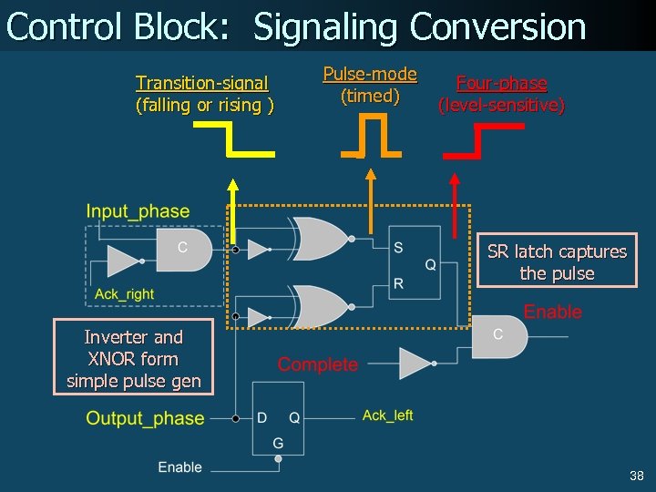 Control Block: Signaling Conversion Transition-signal (falling or rising ) Pulse-mode (timed) Four-phase (level-sensitive) SR latch captures the pulse Inverter and XNOR form simple pulse gen 38
 Timing Requirements ã Circuits almost entirely QDI ã Exceptions: l Control block: Ø Two-sided timing constraint on length of pulse Ø Sensitive to both gate and wire delays Ø Careful layout required l Latches: simple hold time constraints Ø SR latches can be replaced by C-elements – C-elements also have implementation-specific timing constraints – SR latch much faster than our standard cell C-element Ø D latch can be removed at cost of concurrency 39
 Outline ã Motivation and Contribution ã Proposed System Architecture ã Experimental Results l Design Methodology l Datapath Setup l Simulation Results l Latency and Throughput Analysis ã Extensions: Other Signaling Styles ã Conclusions and Future Work 40
 Design Methodology ã Standard cell design flow with complete layout l 0. 18 μm TSMC CMOS process l 4 metal layers of 7 available used in routing ã Custom place-and-route used l Only major layout concern: pulse generator circuit l Design could be automated with constraints on pulse ã Analog simulations: based on layout-extracted design l Test vectors including limiting fast and slow cases 41
 Datapath Implementation ã Two function blocks implemented l An 8 x 8 carry-save multiplier l An empty FIFO stage Ø FIFO contains four-phase completion detector only Ø Demonstrates minimum possible node latency ã Blocks are QDI in evaluate, but “eager” in reset l Implemented in combinational CMOS l “DIMS”-style logic (with C-elements) could be used instead Ø QDI in both directions Ø Increases both forward and reverse latencies 42
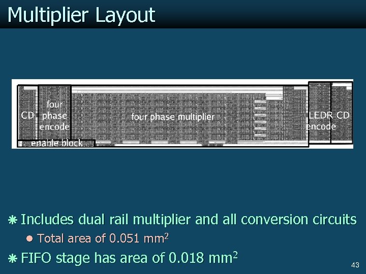 Multiplier Layout ã Includes dual rail multiplier and all conversion circuits l Total area of 0. 051 mm 2 ã FIFO stage has area of 0. 018 mm 2 43
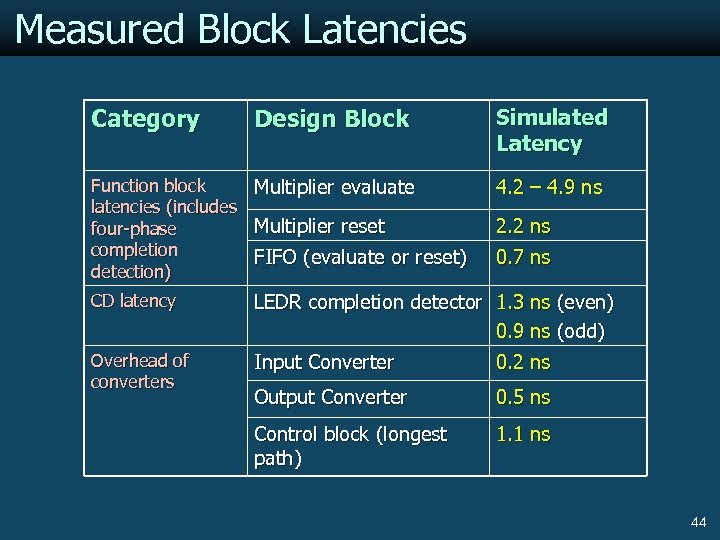 Measured Block Latencies Category Design Block Function block Multiplier evaluate latencies (includes Multiplier reset four-phase completion FIFO (evaluate or reset) detection) Simulated Latency 4. 2 – 4. 9 ns 2. 2 ns 0. 7 ns CD latency LEDR completion detector 1. 3 ns (even) 0. 9 ns (odd) Overhead of converters Input Converter 0. 2 ns Output Converter 0. 5 ns Control block (longest path) 1. 1 ns 44
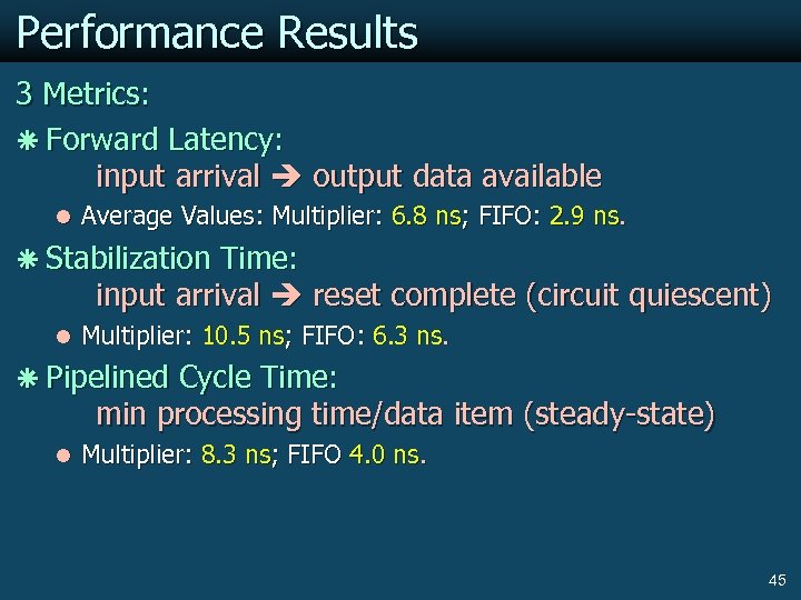 Performance Results 3 Metrics: ã Forward Latency: input arrival output data available l Average Values: Multiplier: 6. 8 ns; FIFO: 2. 9 ns. ã Stabilization Time: input arrival reset complete (circuit quiescent) l Multiplier: 10. 5 ns; FIFO: 6. 3 ns. ã Pipelined Cycle Time: min processing time/data item (steady-state) l Multiplier: 8. 3 ns; FIFO 4. 0 ns. 45
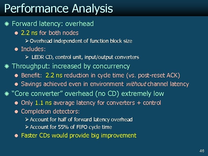 Performance Analysis ã Forward latency: overhead l 2. 2 ns for both nodes Ø Overhead independent of function block size l Includes: Ø LEDR CD, control unit, input/output converters ã Throughput: increased by concurrency l Benefit: 2. 2 ns reduction in cycle time (vs. post-reset ACK) l Savings achieved even in environment without channel latency ã “Core converter” overhead (no CD) extremely low l Only 1. 1 ns average latency for converters + control l Completion detectors: Ø Account for half of forward latency overhead Ø Account for 55% of FIFO cycle time l Faster CDs would provide big improvement 46
 Outline ã Motivation and Contribution ã Proposed System Architecture ã Experimental Results ã Extensions: Other Signaling Styles l Converters for 1 -of-4 function blocks l Converters for bundled data function block ã Conclusions and Future Work 47
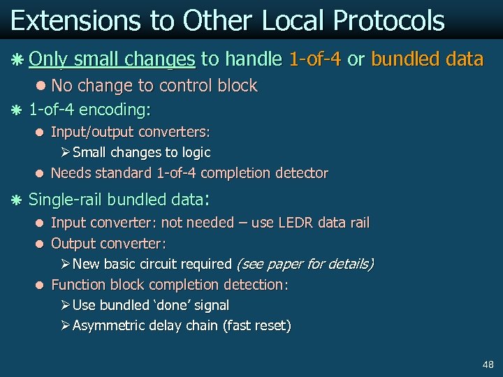 Extensions to Other Local Protocols ã Only small changes to handle 1 -of-4 or bundled data l No change to control block ã 1 -of-4 encoding: l Input/output converters: Ø Small changes to logic l Needs standard 1 -of-4 completion detector ã Single-rail bundled data: l Input converter: not needed – use LEDR data rail l Output converter: Ø New basic circuit required (see paper for details) l Function block completion detection: Ø Use bundled ‘done’ signal Ø Asymmetric delay chain (fast reset) 48
 Outline ã Background and Motivation ã Contribution ã Proposed System Architecture ã Experimental Results ã Extensions: Other Signaling Styles ã Conclusions and Future Work l Summary and Conclusion l Future Work 49
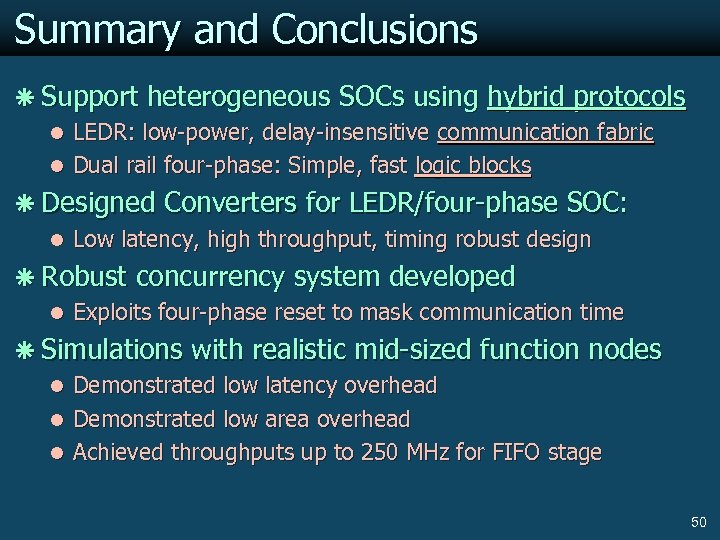 Summary and Conclusions ã Support heterogeneous SOCs using hybrid protocols l LEDR: low-power, delay-insensitive communication fabric l Dual rail four-phase: Simple, fast logic blocks ã Designed Converters for LEDR/four-phase SOC: l Low latency, high throughput, timing robust design ã Robust concurrency system developed l Exploits four-phase reset to mask communication time ã Simulations with realistic mid-sized function nodes l Demonstrated low latency overhead l Demonstrated low area overhead l Achieved throughputs up to 250 MHz for FIFO stage 50
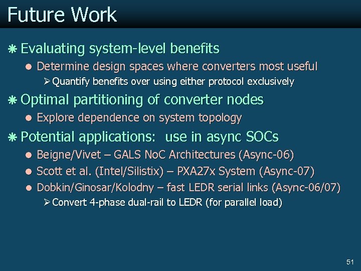 Future Work ã Evaluating system-level benefits l Determine design spaces where converters most useful Ø Quantify benefits over using either protocol exclusively ã Optimal partitioning of converter nodes l Explore dependence on system topology ã Potential applications: use in async SOCs l Beigne/Vivet – GALS No. C Architectures (Async-06) l Scott et al. (Intel/Silistix) – PXA 27 x System (Async-07) l Dobkin/Ginosar/Kolodny – fast LEDR serial links (Async-06/07) Ø Convert 4 -phase dual-rail to LEDR (for parallel load) 51


