1eee5c1f5926ab1e93bdc34e8217acca.ppt
- Количество слайдов: 15
 EEE 2135 Digital Logic Design Chapter 1. Introduction 서강대학교 전자공학과
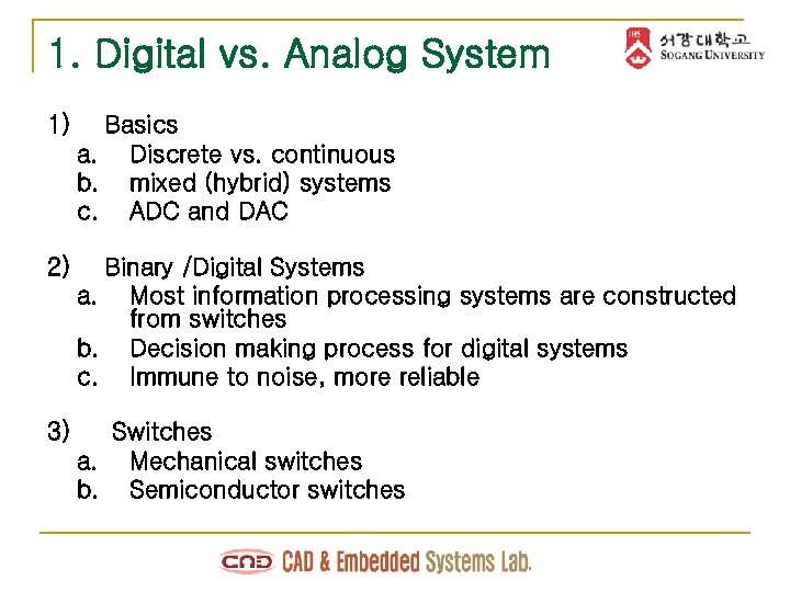 1. Digital vs. Analog System 1) Basics a. Discrete vs. continuous b. mixed (hybrid) systems c. ADC and DAC 2) Binary /Digital Systems a. Most information processing systems are constructed from switches b. Decision making process for digital systems c. Immune to noise, more reliable 3) Switches a. Mechanical switches b. Semiconductor switches
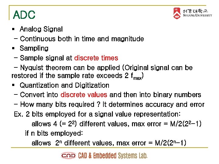 ADC § Analog Signal - Continuous both in time and magnitude § Sampling - Sample signal at discrete times - Nyquist theorem can be applied (Original signal can be restored if the sample rate exceeds 2 fmax) § Quantization and Digitization - Convert into discrete values and then into binary numbers - How many bits required ? It determines accuracy and error Ex. 2 bits employed for a signal value representation: allows 4 (= 22) different values, max error = M/2(22 -1) if n bits employed: allows 2 n different values, max error = M/2(2 n-1)
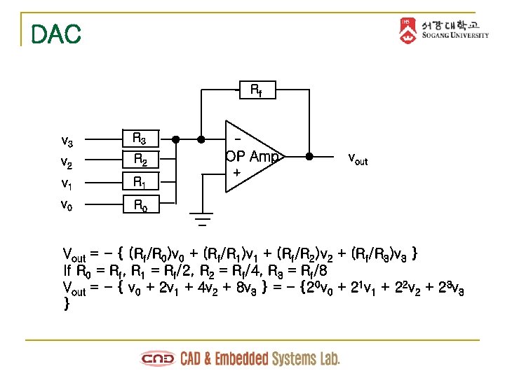 DAC Rf v 3 R 3 v 2 R 2 v 1 R 1 v 0 R 0 - OP Amp vout + Vout = - { (Rf/R 0)v 0 + (Rf/R 1)v 1 + (Rf/R 2)v 2 + (Rf/R 3)v 3 } If R 0 = Rf, R 1 = Rf/2, R 2 = Rf/4, R 3 = Rf/8 Vout = - { v 0 + 2 v 1 + 4 v 2 + 8 v 3 } = - {20 v 0 + 21 v 1 + 22 v 2 + 23 v 3 }
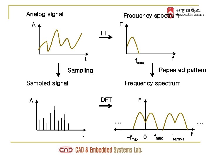 Analog signal Frequency spectrum F A FT t f fmax Repeated pattern Sampling Sampled signal Frequency spectrum DFT A F … t … -fmax 0 fmax fsample f
 2. Behavior and Structure 1) Behavioral Description a. Functionality, input/output relationships b. Truth table, equation, HDL 2) Structure Description a. Functional modules (components) and their interconnections b. Block diagrams c. Schematic diagrams - generic block symbols replaced by symbols with distinctive/standardized shapes
 3. Digital System Design 1) Design a. Refinement process from behavior to structure I. Specification to implementation II. Synthesis (by automated software) b. Design levels I. Designs described at various levels of details or complexity II. Design hierarchy - A non-primitive component Ci at level i can be expanded to a multi-component system at level i-1 c. Hierarchical design I. reduce design complexity II. to partition system into subsystems with manageable size III. To allow concurrent design by team members IV. To use reusable components (libraries)
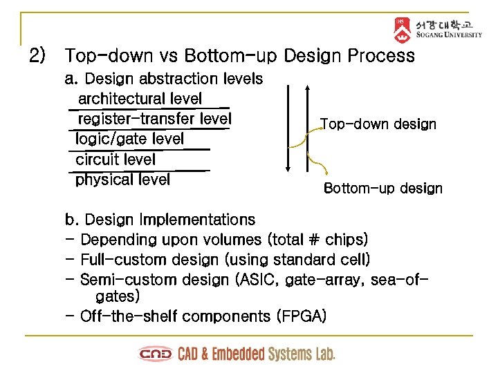 2) Top-down vs Bottom-up Design Process a. Design abstraction levels architectural level register-transfer level logic/gate level circuit level physical level Top-down design Bottom-up design b. Design Implementations - Depending upon volumes (total # chips) - Full-custom design (using standard cell) - Semi-custom design (ASIC, gate-array, sea-ofgates) - Off-the-shelf components (FPGA)
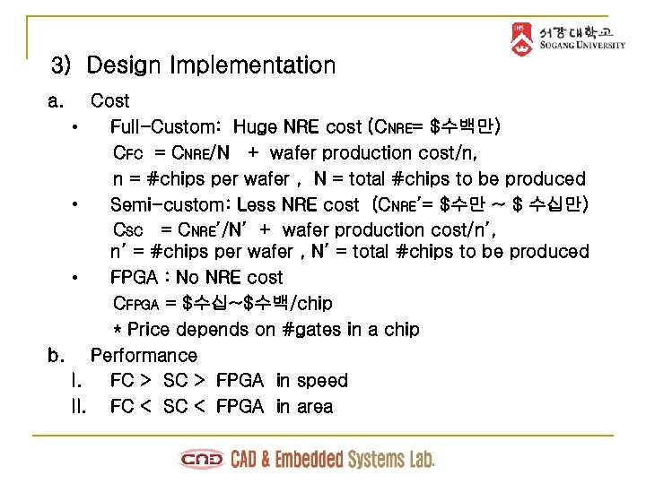 3) Design Implementation a. Cost • Full-Custom: Huge NRE cost (CNRE= $수백만) CFC = CNRE/N + wafer production cost/n, n = #chips per wafer , N = total #chips to be produced • Semi-custom: Less NRE cost (CNRE’= $수만 ~ $ 수십만) CSC = CNRE’/N’ + wafer production cost/n’, n’ = #chips per wafer , N’ = total #chips to be produced • FPGA : No NRE cost CFPGA = $수십~$수백/chip * Price depends on #gates in a chip b. Performance I. FC > SC > FPGA in speed II. FC < SC < FPGA in area
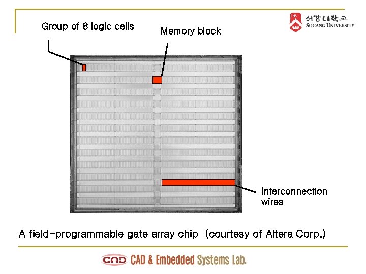 Group of 8 logic cells Memory block Interconnection wires A field-programmable gate array chip (courtesy of Altera Corp. )
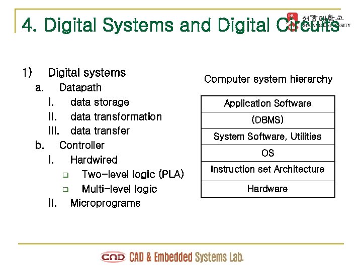 4. Digital Systems and Digital Circuits 1) Digital systems a. Datapath I. data storage II. data transformation III. data transfer b. Controller I. Hardwired q Two-level logic (PLA) q Multi-level logic II. Microprograms Computer system hierarchy Application Software (DBMS) System Software, Utilities OS Instruction set Architecture Hardware
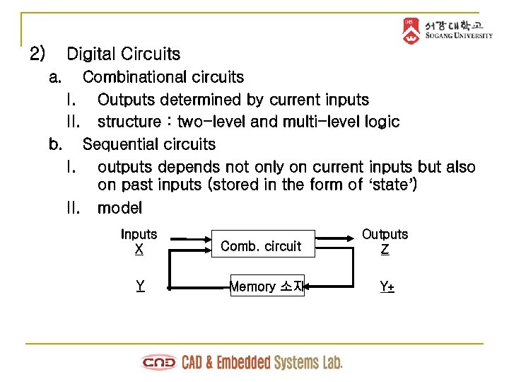 2) Digital Circuits a. Combinational circuits I. Outputs determined by current inputs II. structure : two-level and multi-level logic b. Sequential circuits I. outputs depends not only on current inputs but also on past inputs (stored in the form of ‘state’) II. model Inputs X Y Comb. circuit Memory 소자 Outputs Z Y+
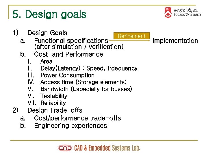 5. Design goals 1) Design Goals Refinement a. Functional specifications (after simulation / verification) b. Cost and Performance I. III. IV. V. VII. 2) Area Delay(Latency) : Speed, frdequency Power Consumption Access time (Storage elements) Bandwidth (Especially for busses) Testability Reliability Design Trade-offs a. Cost/performance trade-offs b. Engineering experiences Implementation
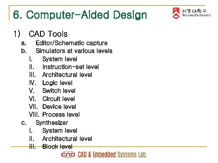 6. Computer-Aided Design 1) CAD Tools a. b. Editor/Schematic capture Simulators at various levels I. System level II. Instruction-set level III. Architectural level IV. Logic level V. Switch level VI. Circuit level VII. Device level VIII. Process level c. Synthesizer I. System level II. Architectural level III. Block level
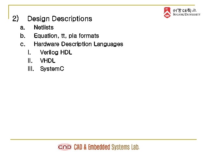 2) Design Descriptions a. b. c. Netlists Equation, tt, pla formats Hardware Description Languages I. Verilog HDL II. VHDL III. System. C


