b69da5a50f67e52d5d4f534896475177.ppt
- Количество слайдов: 61
 EECS 150 - Components and Design Techniques for Digital Systems Lec 9 – Putting it all together… 9 -25 -07 David Culler Electrical Engineering and Computer Sciences University of California, Berkeley http: //www. eecs. berkeley. edu/~culler http: //inst. eecs. berkeley. edu/~cs 150 9/25/07 EECS 150 fa 07 1
 Outline • Top-to-bottom – What have we covered so far? • Combo Lock example – FSM to logic – Mapping to FPGAs • Announcements • Counters revisited • Another example – Ant Brain 9/25/07 EECS 150 fa 07 2
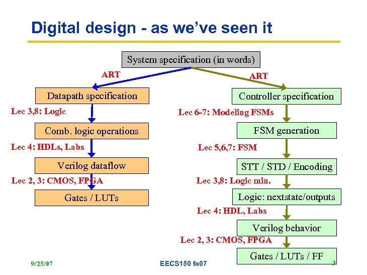 Digital design - as we’ve seen it System specification (in words) ART Datapath specification Lec 3, 8: Logic Controller specification Lec 6 -7: Modeling FSMs FSM generation Comb. logic operations Lec 4: HDLs, Labs Lec 5, 6, 7: FSM Verilog dataflow Lec 2, 3: CMOS, FPGA STT / STD / Encoding Lec 3, 8: Logic min. Logic: nextstate/outputs Gates / LUTs Lec 4: HDL, Labs Verilog behavior Lec 2, 3: CMOS, FPGA 9/25/07 EECS 150 fa 07 Gates / LUTs / FF 3
 Where are we now? • (Synchronous) Sequential systems • Given datapath and control specifications – Generate comb. logic for datapath » Minimize logic for efficient implementation – Generate FSM for controller » Choose implementation, encoding » Generate logic for nextstate and output – Describe datapath and controller in Verilog » structure, dataflow and behavior » Map onto gates or LUTs • Seems like a good point to “test” your understanding! 9/25/07 EECS 150 fa 07 4
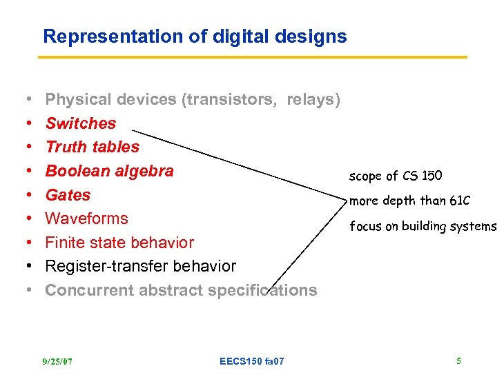 Representation of digital designs • • • Physical devices (transistors, relays) Switches Truth tables Boolean algebra Gates Waveforms Finite state behavior Register-transfer behavior Concurrent abstract specifications 9/25/07 EECS 150 fa 07 scope of CS 150 more depth than 61 C focus on building systems 5
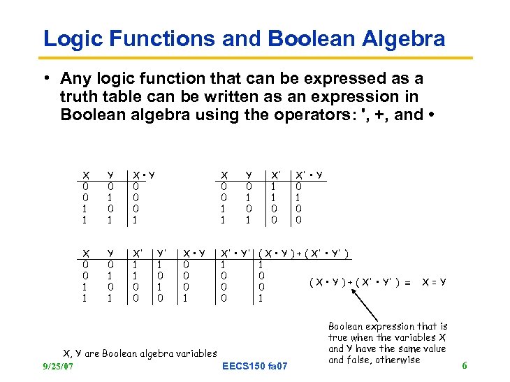 Logic Functions and Boolean Algebra • Any logic function that can be expressed as a truth table can be written as an expression in Boolean algebra using the operators: ', +, and • X 0 0 1 1 Y 0 1 X • Y 0 0 0 1 X 0 0 1 1 Y 0 1 X' 1 1 0 0 X 0 0 1 1 Y' 1 0 X • Y 0 0 0 1 Y 0 1 X' • Y' 1 0 0 0 X' 1 1 0 0 X' • Y 0 1 0 0 ( X • Y ) + ( X' • Y' ) 1 0 ( X • Y ) + ( X' • Y' ) º 0 1 X, Y are Boolean algebra variables 9/25/07 EECS 150 fa 07 X = Y Boolean expression that is true when the variables X and Y have the same value and false, otherwise 6
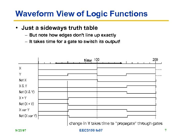 Waveform View of Logic Functions • Just a sideways truth table – But note how edges don't line up exactly – It takes time for a gate to switch its output! time change in Y takes time to "propagate" through gates 9/25/07 EECS 150 fa 07 7
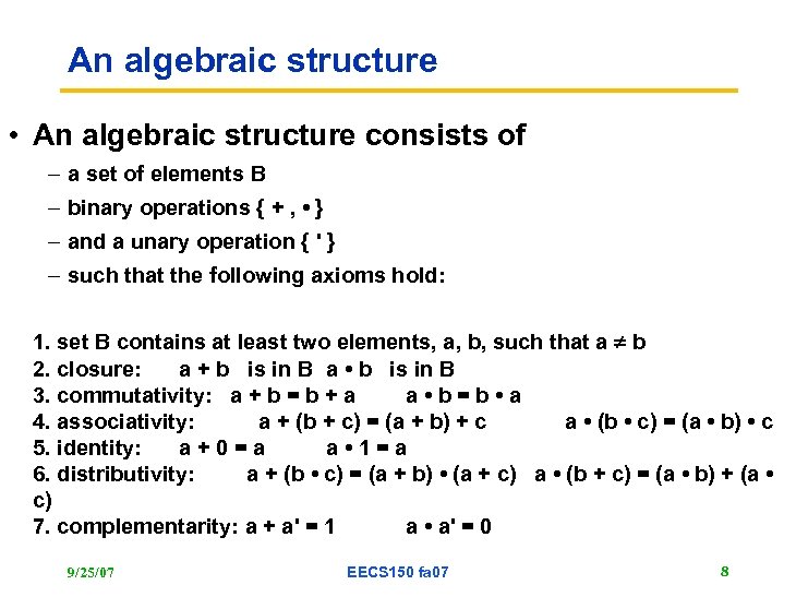 An algebraic structure • An algebraic structure consists of – a set of elements B – binary operations { + , • } – and a unary operation { ' } – such that the following axioms hold: 1. set B contains at least two elements, a, b, such that a b 2. closure: a + b is in B a • b is in B 3. commutativity: a + b = b + a a • b=b • a 4. associativity: a + (b + c) = (a + b) + c a • (b • c) = (a • b) • c 5. identity: a+0=a a • 1=a 6. distributivity: a + (b • c) = (a + b) • (a + c) a • (b + c) = (a • b) + (a • c) 7. complementarity: a + a' = 1 a • a' = 0 9/25/07 EECS 150 fa 07 8
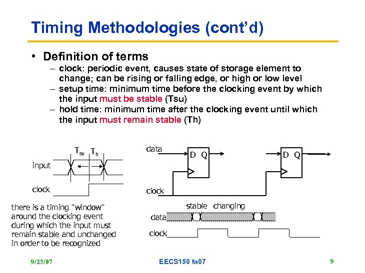 Timing Methodologies (cont’d) • Definition of terms – clock: periodic event, causes state of storage element to change; can be rising or falling edge, or high or low level – setup time: minimum time before the clocking event by which the input must be stable (Tsu) – hold time: minimum time after the clocking event until which the input must remain stable (Th) Tsu Th data D Q input clock there is a timing "window" around the clocking event during which the input must remain stable and unchanged in order to be recognized 9/25/07 clock stable changing data clock EECS 150 fa 07 9
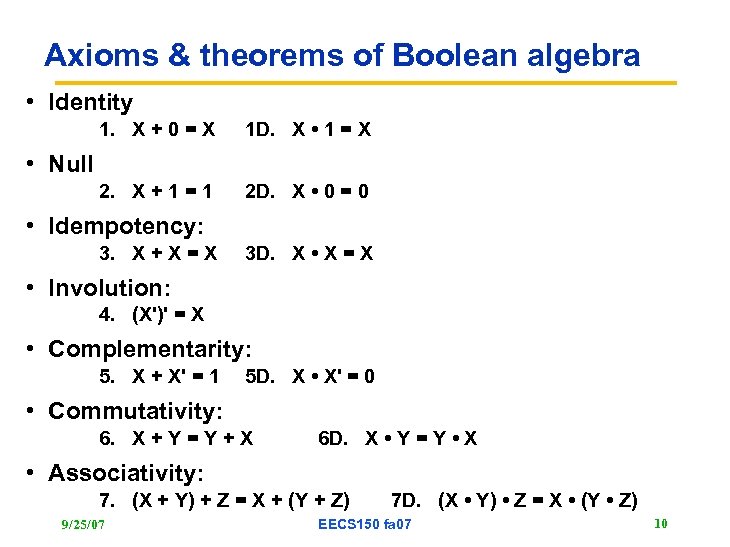 Axioms & theorems of Boolean algebra • Identity 1. X + 0 = X 1 D. X • 1 = X 2. X + 1 = 1 2 D. X • 0 = 0 • Null • Idempotency: 3. X + X = X 3 D. X • X = X • Involution: 4. (X')' = X • Complementarity: 5. X + X' = 1 5 D. X • X' = 0 • Commutativity: 6. X + Y = Y + X 6 D. X • Y = Y • X • Associativity: 7. (X + Y) + Z = X + (Y + Z) 9/25/07 7 D. (X • Y) • Z = X • (Y • Z) EECS 150 fa 07 10
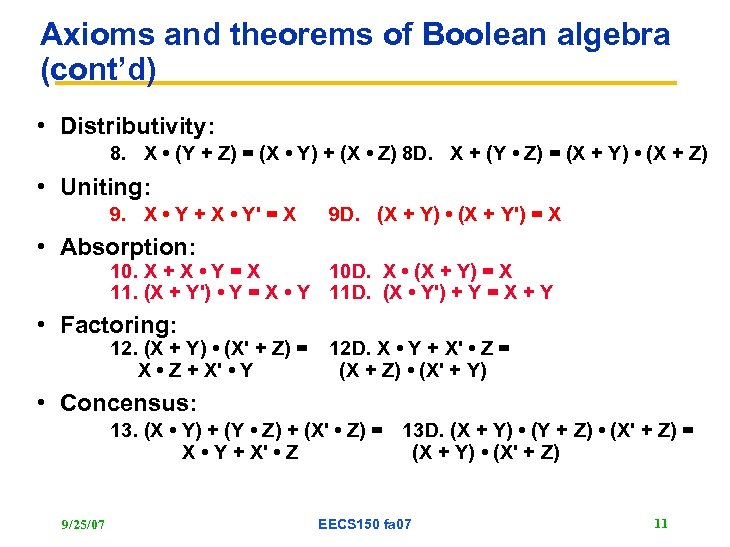 Axioms and theorems of Boolean algebra (cont’d) • Distributivity: 8. X • (Y + Z) = (X • Y) + (X • Z) 8 D. X + (Y • Z) = (X + Y) • (X + Z) • Uniting: 9. X • Y + X • Y' = X 9 D. (X + Y) • (X + Y') = X • Absorption: 10. X + X • Y = X 10 D. X • (X + Y) = X 11. (X + Y') • Y = X • Y 11 D. (X • Y') + Y = X + Y • Factoring: 12. (X + Y) • (X' + Z) = X • Z + X' • Y 12 D. X • Y + X' • Z = (X + Z) • (X' + Y) • Concensus: 13. (X • Y) + (Y • Z) + (X' • Z) = 13 D. (X + Y) • (Y + Z) • (X' + Z) = X • Y + X' • Z (X + Y) • (X' + Z) 9/25/07 EECS 150 fa 07 11
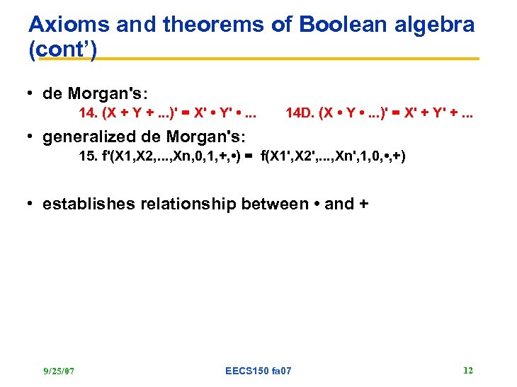 Axioms and theorems of Boolean algebra (cont’) • de Morgan's: 14. (X + Y +. . . )' = X' • Y' • . . . 14 D. (X • Y • . . . )' = X' + Y' +. . . • generalized de Morgan's: 15. f'(X 1, X 2, . . . , Xn, 0, 1, +, • ) = f(X 1', X 2', . . . , Xn', 1, 0, • , +) • establishes relationship between • and + 9/25/07 EECS 150 fa 07 12
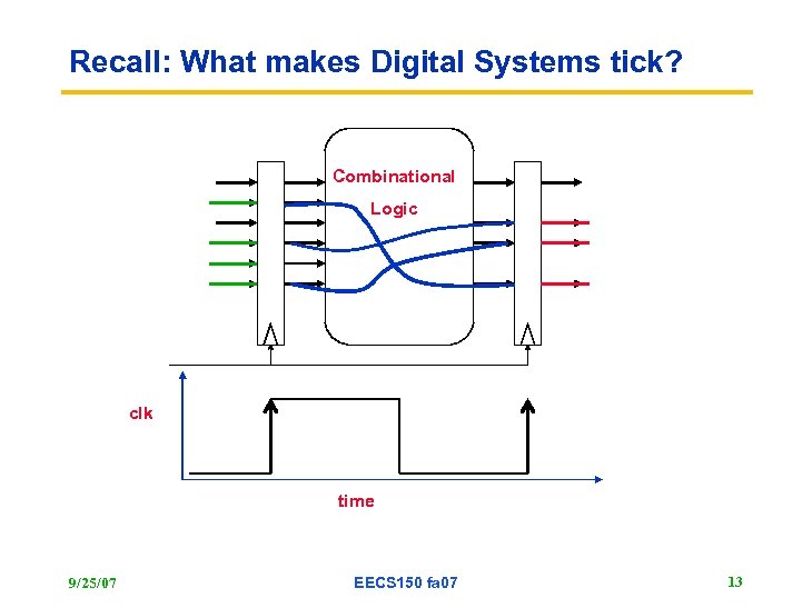 Recall: What makes Digital Systems tick? Combinational Logic clk time 9/25/07 EECS 150 fa 07 13
 Sequential Logic Implementation • Models for representing sequential circuits – Finite-state machines (Moore and Mealy) – Representation of memory (states) – Changes in state (transitions) • Design procedure – – – 9/25/07 State diagrams Implementation choice: counters, shift registers, FSM State transition table State encoding Combinational logic » Next state functions » Output functions EECS 150 fa 07 14
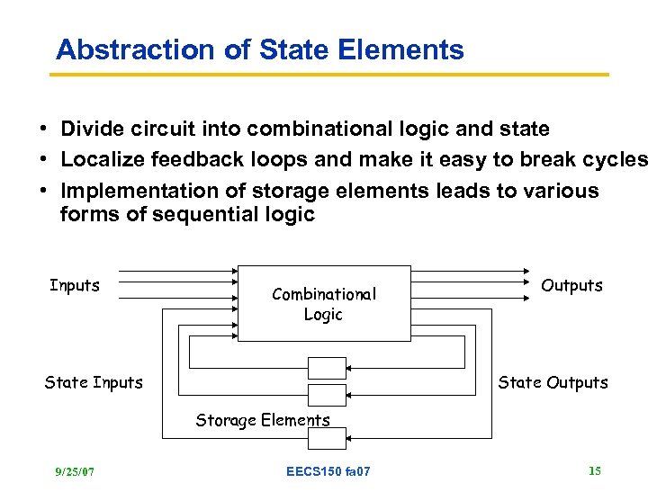 Abstraction of State Elements • Divide circuit into combinational logic and state • Localize feedback loops and make it easy to break cycles • Implementation of storage elements leads to various forms of sequential logic Inputs Combinational Logic State Inputs Outputs State Outputs Storage Elements 9/25/07 EECS 150 fa 07 15
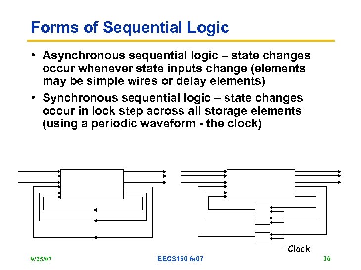 Forms of Sequential Logic • Asynchronous sequential logic – state changes occur whenever state inputs change (elements may be simple wires or delay elements) • Synchronous sequential logic – state changes occur in lock step across all storage elements (using a periodic waveform - the clock) Clock 9/25/07 EECS 150 fa 07 16
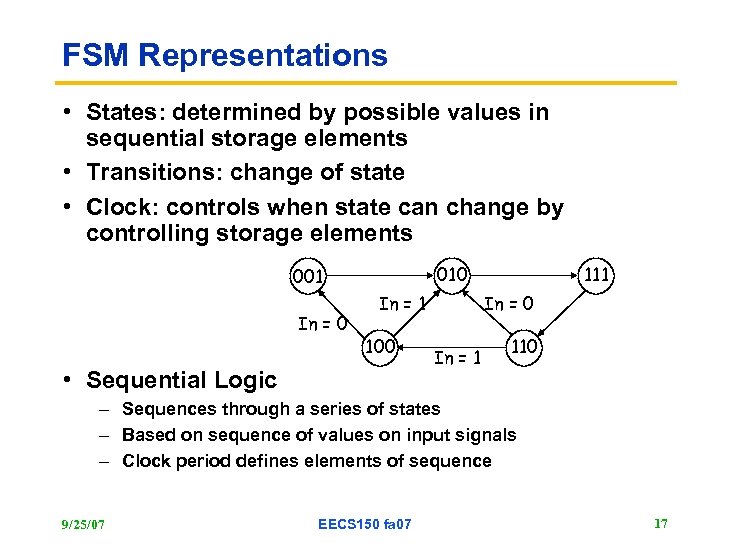 FSM Representations • States: determined by possible values in sequential storage elements • Transitions: change of state • Clock: controls when state can change by controlling storage elements 010 001 In = 0 In = 1 100 • Sequential Logic 111 In = 0 In = 1 110 – Sequences through a series of states – Based on sequence of values on input signals – Clock period defines elements of sequence 9/25/07 EECS 150 fa 07 17
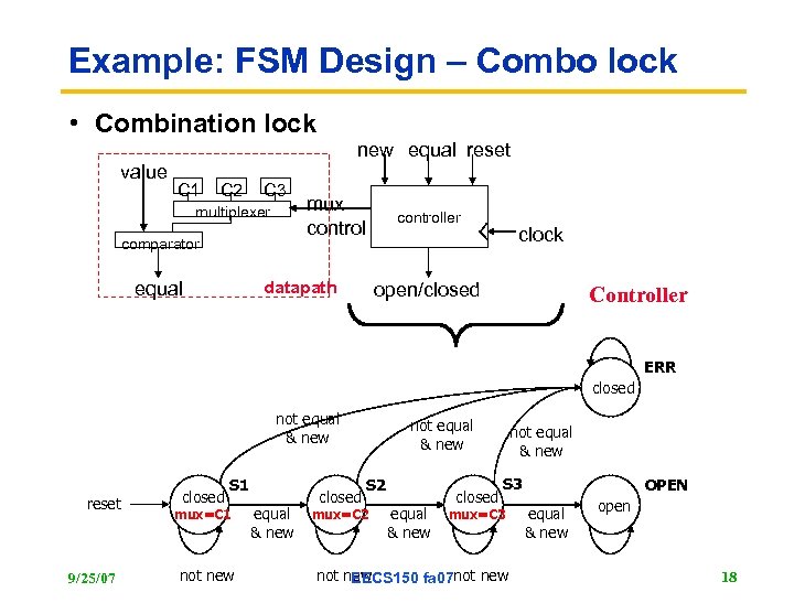 Example: FSM Design – Combo lock • Combination lock new equal reset value C 1 C 2 C 3 multiplexer comparator mux controller datapath equal clock open/closed Controller ERR closed not equal & new reset 9/25/07 closed S 1 mux=C 1 not new equal & new closed not equal & new S 2 mux=C 2 equal & new closed not equal & new S 3 mux=C 3 not new EECS 150 fa 07 not new OPEN equal & new open 18
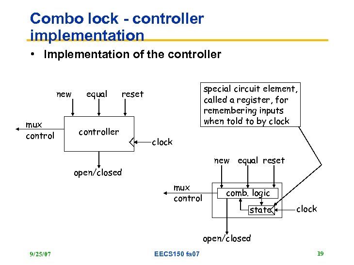 Combo lock - controller implementation • Implementation of the controller new mux control equal special circuit element, called a register, for remembering inputs when told to by clock reset controller clock new equal reset open/closed mux control comb. logic state clock open/closed 9/25/07 EECS 150 fa 07 19
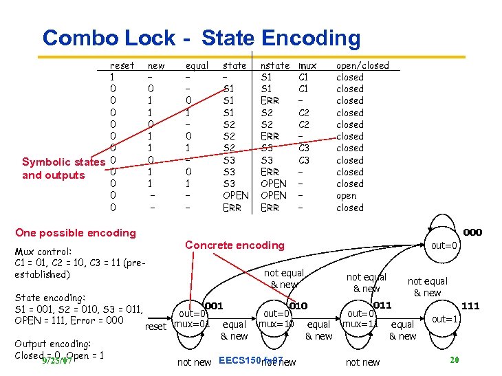 Combo Lock - State Encoding reset 1 0 0 0 Symbolic states 0 0 and outputs 0 0 0 new – 0 1 1 – – equal – – 0 1 – – state – S 1 S 1 S 2 S 2 S 3 S 3 OPEN ERR nstate S 1 ERR S 2 ERR S 3 ERR OPEN ERR mux C 1 – C 2 – C 3 – – open/closed closed closed open closed 000 One possible encoding Mux control: C 1 = 01, C 2 = 10, C 3 = 11 (preestablished) State encoding: S 1 = 001, S 2 = 010, S 3 = 011, OPEN = 111, Error = 000 Output encoding: Closed 9/25/07 = 0, Open = 1 Concrete encoding not equal & new 001 out=0 reset mux=01 equal & new 010 out=0 mux=10 equal & new fa 07 not new EECS 150 not new out=0 not equal & new 011 out=0 mux=11 equal & new not new 111 out=1 20
 FSM implementation • Steps for the hardware designer: – – Word specification FSM design Encoding Verification! • At this point, hand over to synthesis tools: – Describe FSM behavior in Verilog – Synthesize controller • Good encoding – – Better performance Fewer state bits Possibility of state minimization Tools also try to figure this out For this example, go through the logic synthesis steps (ideally, tools take care of all this)… fa 07 9/25/07 EECS 150 21
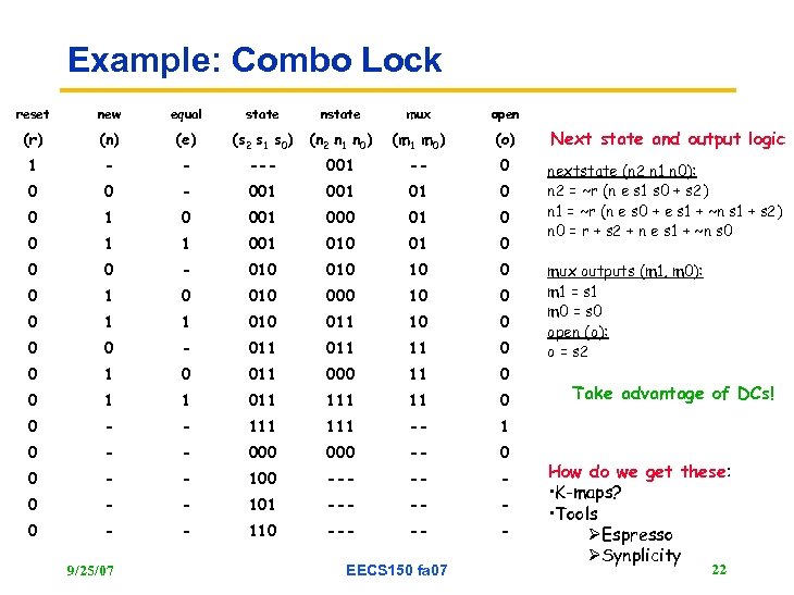 Example: Combo Lock reset new equal state nstate mux open (r) (n) (e) (s 2 s 1 s 0) (n 2 n 1 n 0) (m 1 m 0) (o) Next state and output logic 1 - - --- 001 -- 0 0 0 - 001 01 0 001 000 01 0 0 1 1 001 010 01 0 nextstate (n 2 n 1 n 0): n 2 = ~r (n e s 1 s 0 + s 2) n 1 = ~r (n e s 0 + e s 1 + ~n s 1 + s 2) n 0 = r + s 2 + n e s 1 + ~n s 0 0 0 - 010 10 0 0 1 0 010 000 10 0 0 1 1 010 011 10 0 - 011 11 0 011 000 11 0 0 1 1 011 11 0 0 - - 111 -- 1 0 - - 000 -- 0 0 - - 100 --- -- - 0 - - 101 --- -- - 0 - - 110 --- -- - 9/25/07 EECS 150 fa 07 mux outputs (m 1, m 0): m 1 = s 1 m 0 = s 0 open (o): o = s 2 Take advantage of DCs! How do we get these: • K-maps? • Tools ØEspresso ØSynplicity 22
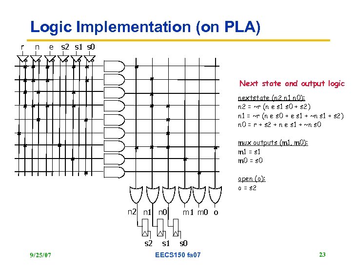 Logic Implementation (on PLA) r n e s 2 s 1 s 0 Next state and output logic nextstate (n 2 n 1 n 0): n 2 = ~r (n e s 1 s 0 + s 2) n 1 = ~r (n e s 0 + e s 1 + ~n s 1 + s 2) n 0 = r + s 2 + n e s 1 + ~n s 0 mux outputs (m 1, m 0): m 1 = s 1 m 0 = s 0 open (o): o = s 2 n 1 n 0 s 2 9/25/07 s 1 m 0 o s 0 EECS 150 fa 07 23
 Alternate logic implementations • PALs • Multi-level circuits – Library of gates for implementation technology • LUTs on FPGA • … 9/25/07 EECS 150 fa 07 24
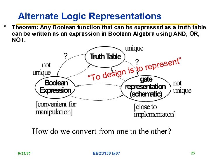 Alternate Logic Representations * Theorem: Any Boolean function that can be expressed as a truth table can be written as an expression in Boolean Algebra using AND, OR, NOT. esent” to repr ign is o des “T How do we convert from one to the other? 9/25/07 EECS 150 fa 07 25
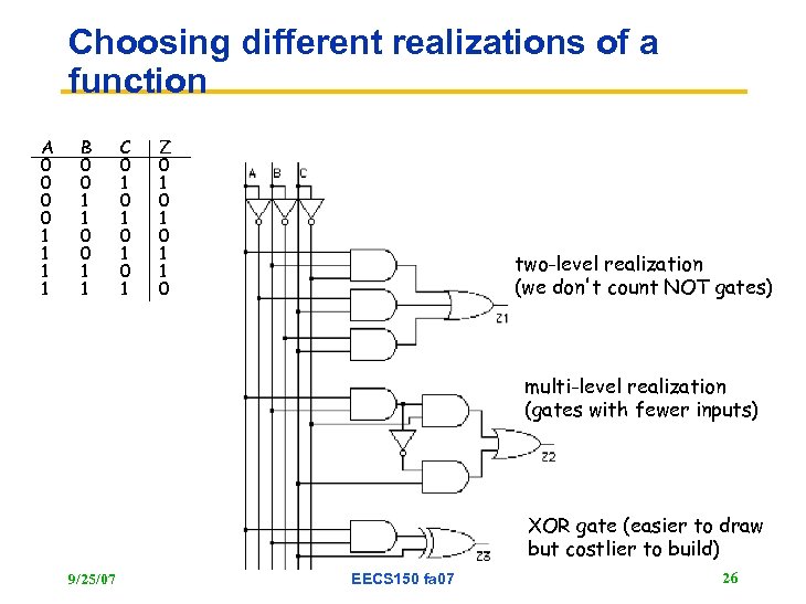 Choosing different realizations of a function A 0 0 1 1 B 0 0 1 1 C 0 1 0 1 Z 0 1 0 1 1 0 two-level realization (we don't count NOT gates) multi-level realization (gates with fewer inputs) XOR gate (easier to draw but costlier to build) 9/25/07 EECS 150 fa 07 26
 Which realization is best? • Reduce number of inputs – literal: input variable (complemented or not) » approximate cost of logic gate is 2 transistors per literal – Fewer literals means less transistors - smaller circuits – Fewer inputs implies faster gates – Fan-ins (# of gate inputs) are limited in some technologies • Reduce number of gates – Fewer gates (and the packages they come in) means smaller circuits • Reduce number of levels of gates – Fewer level of gates implies reduced signal propagation delays • How do we explore tradeoffs between increased circuit delay and size? – Automated tools to generate different solutions – Logic minimization: reduce number of gates and complexity – Logic optimization: reduction while trading off against delay 9/25/07 EECS 150 fa 07 27
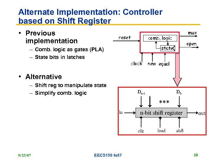 Alternate Implementation: Controller based on Shift Register • Previous implementation reset mux comb. logic open state – Comb. logic as gates (PLA) – State bits in latches clock new equal • Alternative – Shift reg to manipulate state – Simplify comb. logic Dn-1 D 0 *** in n-bit shift register clk 9/25/07 EECS 150 fa 07 load out shft 28
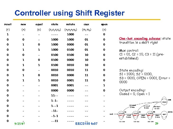 Controller using Shift Register reset new equal state nstate mux open (r) (n) (e) (s 3 s 2 s 1 s 0) (n 3 n 2 n 1 n 0) (m 1 m 0) (o) 1 - - ---- 1000 -- 0 0 0 - 1000 01 0 0 1 1 1000 01 0 0 0 - 0100 10 0 0 1 0 0100 0000 10 0 0 1 1 0100 0010 10 0 - 0010 11 0 0010 0000 11 0 0 1 1 0010 0001 11 0 0 - - 0001 -- 1 0 - - 0000 -- 0 0 - - 11 -- -- - 0 - - 1 -1 - ---- -- - 0 - - 1 --1 ---- -- - 0 - - -11 - ---- -- - 0 - - -1 -1 ---- --11 ---- -- - 0 9/25/07 EECS 150 fa 07 One-hot encoding scheme: state transition is a shift right Mux control: C 1 = 01, C 2 = 10, C 3 = 11 (preestablished) State encoding: S 1 = 1000, S 2 = 0100, S 3 = 0010, OPEN = 0001, Error = 0000 Output encoding: Closed = 0, Open = 1 29
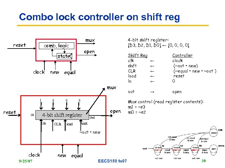 Combo lock controller on shift reg reset mux comb. logic open state clock new 4 -bit shift register: [D 3, D 2, D 1, D 0] ← [0, 0, 0, 0] equal mux 1 reset in 0 0 0 4 -bit shift register clk CLR load open Shift Reg clk ← shft ← CLR ← load ← in ← Controller clock (~out • new) (~equal • new • ~out ) reset 0 out open → Mux control (read register contents): m 1 = ~s 3 m 0 = ~s 2 out shft ~out • new clock 9/25/07 new equal EECS 150 fa 07 30
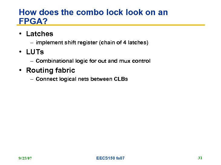 How does the combo lock look on an FPGA? • Latches – implement shift register (chain of 4 latches) • LUTs – Combinational logic for out and mux control • Routing fabric – Connect logical nets between CLBs 9/25/07 EECS 150 fa 07 31
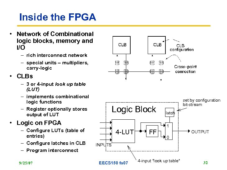 Inside the FPGA • Network of Combinational logic blocks, memory and I/O – rich interconnect network – special units – multipliers, carry-logic • CLBs – 3 or 4 -input look up table (LUT) – implements combinational logic functions – Register optionally stores output of LUT Logic Block • Logic on FPGA – Configure LUTs (table of entries) – Configure latches in CLB – Program interconnect 9/25/07 4 -LUT FF set by configuration bit-stream latch 1 OUTPUT 0 INPUTS EECS 150 fa 07 4 -input "look up table" 32
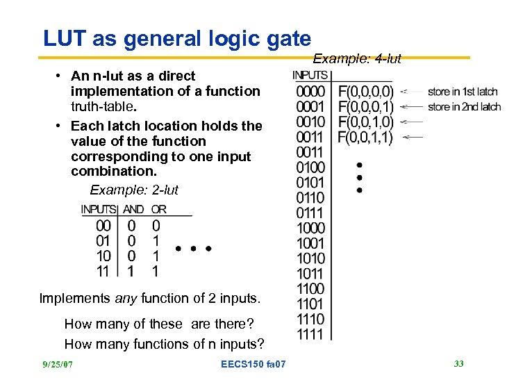 LUT as general logic gate Example: 4 -lut • An n-lut as a direct implementation of a function truth-table. • Each latch location holds the value of the function corresponding to one input combination. Example: 2 -lut Implements any function of 2 inputs. How many of these are there? How many functions of n inputs? 9/25/07 EECS 150 fa 07 33
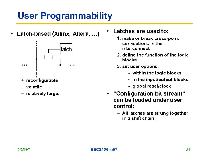 User Programmability • Latch-based (Xilinx, Altera, …) + reconfigurable – volatile – relatively large. • Latches are used to: 1. make or break cross-point connections in the interconnect 2. define the function of the logic blocks 3. set user options: » within the logic blocks » in the input/output blocks » global reset/clock • “Configuration bit stream” can be loaded under user control: – All latches are strung together in a shift chain: 9/25/07 EECS 150 fa 07 34
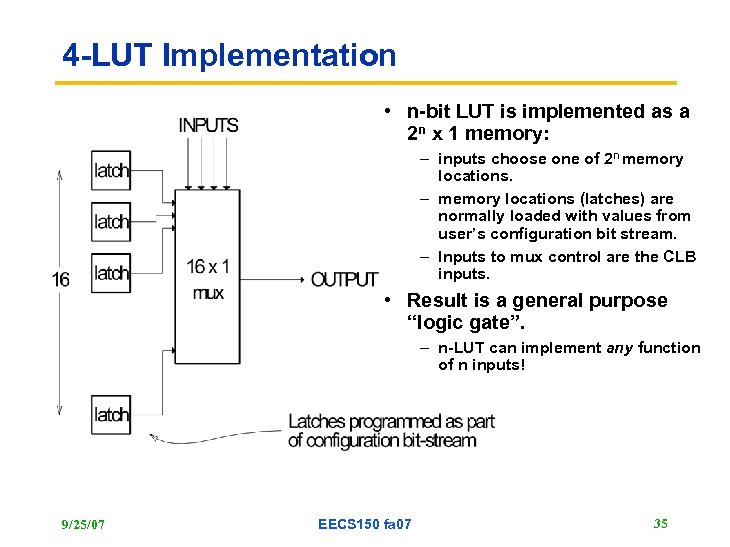 4 -LUT Implementation • n-bit LUT is implemented as a 2 n x 1 memory: – inputs choose one of 2 n memory locations. – memory locations (latches) are normally loaded with values from user’s configuration bit stream. – Inputs to mux control are the CLB inputs. • Result is a general purpose “logic gate”. – n-LUT can implement any function of n inputs! 9/25/07 EECS 150 fa 07 35
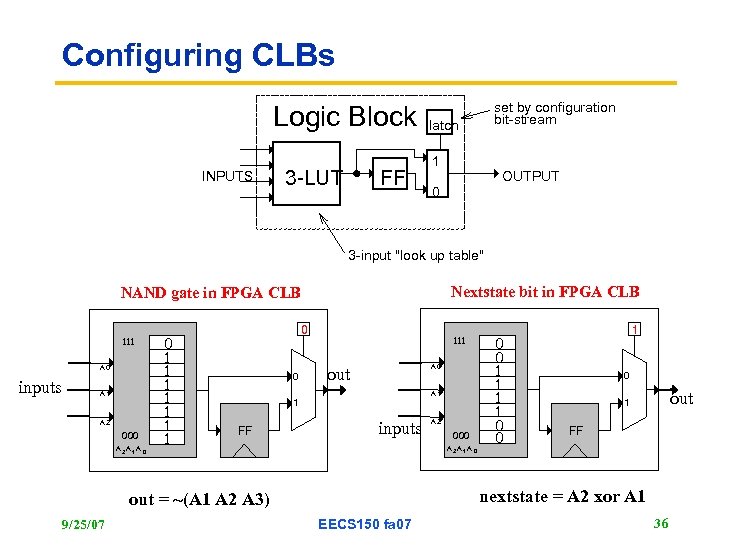 Configuring CLBs Logic Block INPUTS 3 -LUT FF set by configuration bit-stream latch 1 OUTPUT 0 3 -input "look up table" Nextstate bit in FPGA CLB NAND gate in FPGA CLB 0 1 1 1 111 A 0 inputs A 1 A 2 000 A 2 A 1 A 0 0 A 0 out A 1 1 FF inputs A 2 000 A 2 A 1 A 0 1 0 out 1 FF 0 nextstate = A 2 xor A 1 out = ~(A 1 A 2 A 3) 9/25/07 0 0 1 1 0 0 111 EECS 150 fa 07 36
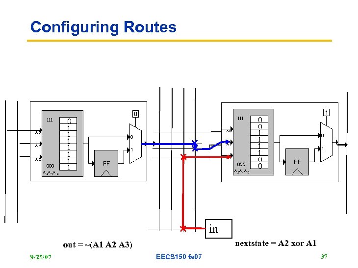 Configuring Routes 0 1 1 1 111 A 0 A 1 A 2 000 A 2 A 1 A 0 0 0 1 1 0 0 111 A 0 0 A 1 1 A 2 FF 000 A 2 A 1 A 0 1 FF 0 in nextstate = A 2 xor A 1 out = ~(A 1 A 2 A 3) 9/25/07 EECS 150 fa 07 37
 Sequential Systems – more examples • Beat the combo lock example to death – Direct FSM implementation – Shift register » Multiple logic representations » gates to LUTs • Up next – A few quick counter examples – Another design problem – Ant Brain 9/25/07 EECS 150 fa 07 38
 Announcements/Reminders • First mid term – Thursday 9/27 – – No notes (… to discuss) Review materials are in the HW 4 Review session tonight 8 -10 Trying to make the exams routine 642 -WALK (9255) • Feel free to approach us with questions… • No discussion Thurs, yes friday • Lab 5 – Where’s the music? – Normal lab lecture on Friday 9/25/07 EECS 150 fa 07 39
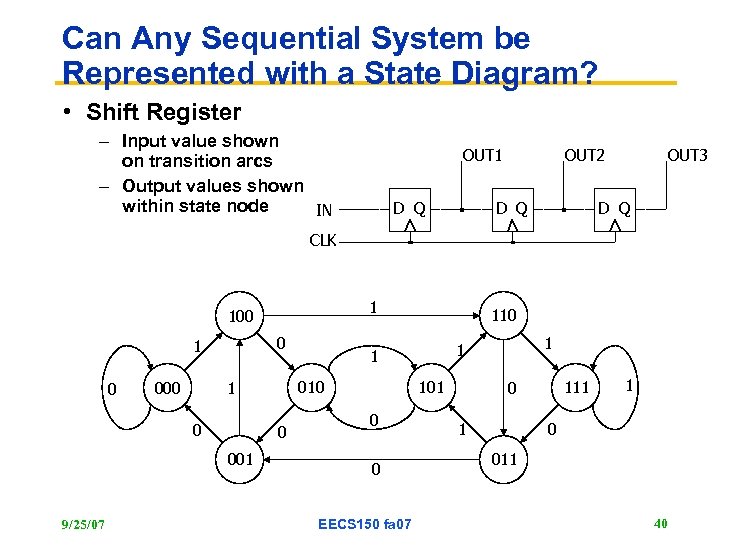 Can Any Sequential System be Represented with a State Diagram? • Shift Register – Input value shown on transition arcs – Output values shown within state node IN OUT 1 D Q OUT 2 D Q OUT 3 D Q CLK 1 100 0 1 0 001 9/25/07 101 0 0 EECS 150 fa 07 1 1 1 010 1 000 111 0 1 1 0 011 40
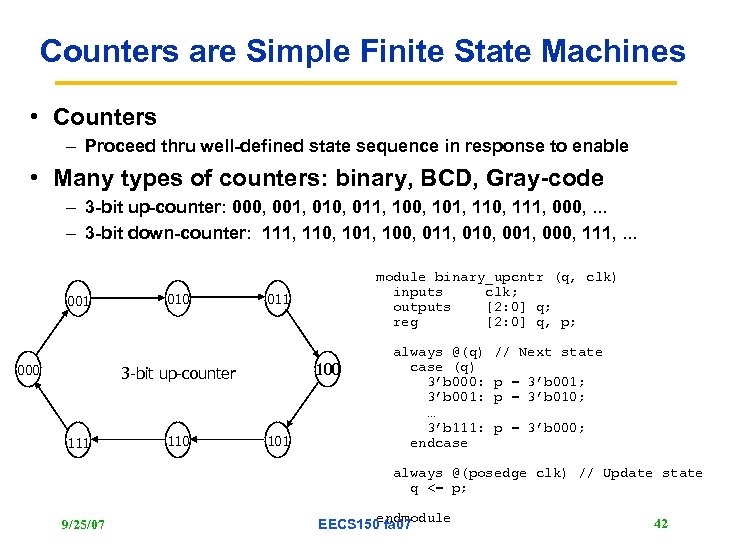 Counters are Simple Finite State Machines • Counters – Proceed thru well-defined state sequence in response to enable • Many types of counters: binary, BCD, Gray-code – 3 -bit up-counter: 000, 001, 010, 011, 100, 101, 110, 111, 000, . . . – 3 -bit down-counter: 111, 110, 101, 100, 011, 010, 001, 000, 111, . . . 001 000 011 100 3 -bit up-counter 111 110 module binary_upcntr (q, clk) inputs clk; outputs [2: 0] q; reg [2: 0] q, p; 101 always @(q) case (q) 3’b 000: 3’b 001: … 3’b 111: endcase // Next state p = 3’b 001; p = 3’b 010; p = 3’b 000; always @(posedge clk) // Update state q <= p; 9/25/07 endmodule EECS 150 fa 07 42
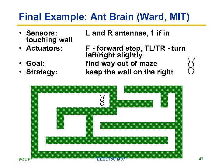 Final Example: Ant Brain (Ward, MIT) • Sensors: touching wall • Actuators: • Goal: • Strategy: 9/25/07 L and R antennae, 1 if in F - forward step, TL/TR - turn left/right slightly find way out of maze keep the wall on the right EECS 150 fa 07 47
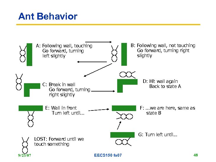 Ant Behavior B: Following wall, not touching Go forward, turning right slightly A: Following wall, touching Go forward, turning left slightly D: Hit wall again Back to state A C: Break in wall Go forward, turning right slightly E: Wall in front Turn left until. . . F: . . . we are here, same as state B G: Turn left until. . . LOST: Forward until we touch something 9/25/07 EECS 150 fa 07 48
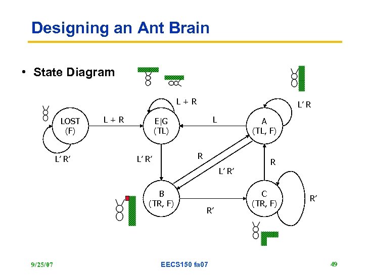 Designing an Ant Brain • State Diagram L+R LOST (F) L’ R’ L+R L’ R L E|G (TL) A (TL, F) R L’ R’ B (TR, F) 9/25/07 R’ EECS 150 fa 07 R C (TR, F) R’ 49
 Synthesizing the Ant Brain Circuit • Encode States Using a Set of State Variables – Arbitrary choice - may affect cost, speed • Use Transition Truth Table – Define next state function for each state variable – Define output function for each output • Implement next state and output functions using combinational logic – 2 -level logic (ROM/PLA/PAL) – Multi-level logic – Next state and output functions can be optimized together 9/25/07 EECS 150 fa 07 50
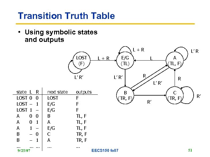 Transition Truth Table • Using symbolic states and outputs L+R LOST (F) L’ R’ E/G (TL) L+R L’ R’ L’ R A (TL, F) L R L’ R’ state LOST A A A B B. . . L 0 – 1 0 0 1 – –. . . 9/25/07 R 0 1 – 0 1. . . next state LOST E/G B A E/G C A. . . outputs F F F TL, F TR, F. . . B (TR, F) EECS 150 fa 07 R’ R C (TR, F) R’ 51
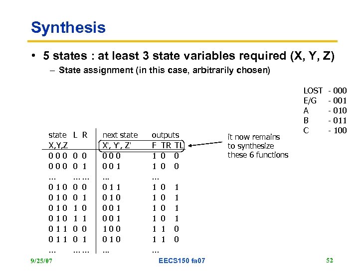 Synthesis • 5 states : at least 3 state variables required (X, Y, Z) – State assignment (in this case, arbitrarily chosen) state X, Y, Z 000. . . 010 010 011. . . 9/25/07 L R 0 0 0 1. . . 0 0 0 1 1 0 0 0 1. . . next state X', Y', Z' 000 001. . . 011 010 001 100 010. . . outputs F TR TL 1 0 0. . . 1 0 1 1 1 0. . . EECS 150 fa 07 it now remains to synthesize these 6 functions LOST E/G A B C - 52 000 001 010 011 100
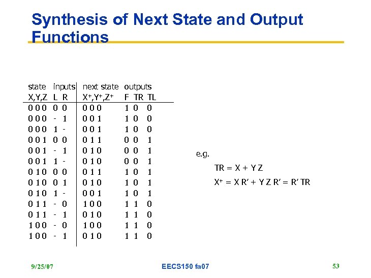 Synthesis of Next State and Output Functions state X, Y, Z 000 000 001 001 010 010 011 100 9/25/07 inputs L R 0 0 - 1 1 0 0 0 1 1 - 0 - 1 next state X+, Y+, Z+ 000 001 011 010 001 100 010 outputs F TR TL 1 0 0 1 0 0 1 1 0 1 1 0 e. g. TR = X + Y Z X+ = X R’ + Y Z R’ = R’ TR EECS 150 fa 07 53
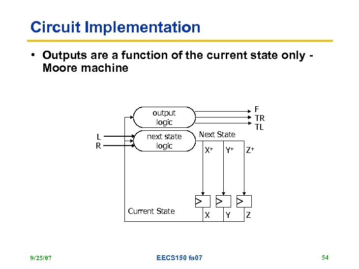 Circuit Implementation • Outputs are a function of the current state only Moore machine F TR TL output logic L R next state logic Next State Current State 9/25/07 EECS 150 fa 07 X+ Y+ Z+ X Y Z 54
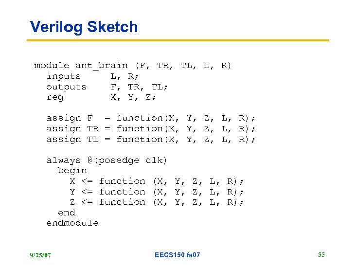 Verilog Sketch module ant_brain (F, TR, TL, L, R) inputs L, R; outputs F, TR, TL; reg X, Y, Z; assign F = function(X, Y, Z, L, R); assign TR = function(X, Y, Z, L, R); assign TL = function(X, Y, Z, L, R); always @(posedge clk) begin X <= function (X, Y, Z, L, R); Y <= function (X, Y, Z, L, R); Z <= function (X, Y, Z, L, R); endmodule 9/25/07 EECS 150 fa 07 55
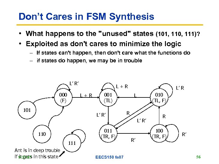 Don’t Cares in FSM Synthesis • What happens to the "unused" states (101, 110, 111)? • Exploited as don't cares to minimize the logic – If states can't happen, then don't care what the functions do – if states do happen, we may be in trouble L’ R’ 000 (F) L+R 101 001 (TL) L’ R’ L’ R 010 (TL, F) L R L’ R’ 011 (TR, F) 110 111 Ant is in deep trouble if 9/25/07 in this state it gets EECS 150 fa 07 R’ R 100 (TR, F) R’ 56
 State Minimization • Fewer states may mean fewer state variables • High-level synthesis may generate many redundant states • Two state are equivalent if they are impossible to distinguish from the outputs of the FSM, i. e. , for any input sequence the outputs are the same • Two conditions for two states to be equivalent: – 1) Output must be the same in both states – 2) Must transition to equivalent states for all input combinations 9/25/07 EECS 150 fa 07 57
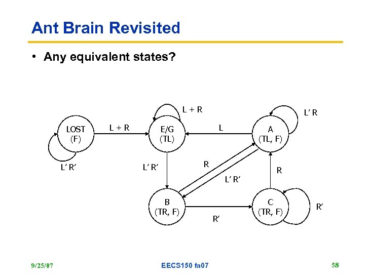 Ant Brain Revisited • Any equivalent states? L+R LOST (F) L’ R’ L+R L’ R L E/G (TL) A (TL, F) R L’ R’ B (TR, F) 9/25/07 EECS 150 fa 07 R’ R C (TR, F) R’ 58
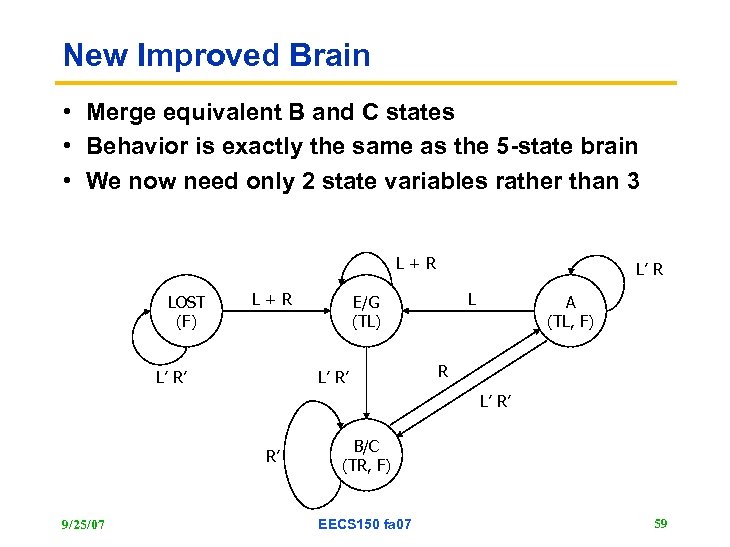 New Improved Brain • Merge equivalent B and C states • Behavior is exactly the same as the 5 -state brain • We now need only 2 state variables rather than 3 L+R LOST (F) L+R L’ R’ L’ R L E/G (TL) L’ R’ A (TL, F) R L’ R’ R’ 9/25/07 B/C (TR, F) EECS 150 fa 07 59
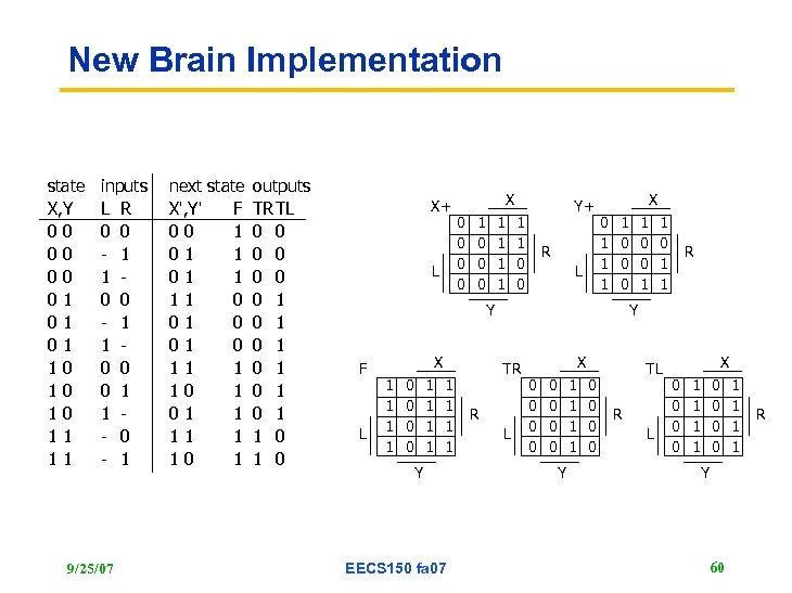 New Brain Implementation state X, Y 00 00 00 01 01 01 10 10 10 11 11 inputs L R 0 0 - 1 1 0 0 0 1 1 - 0 - 1 9/25/07 next state outputs X', Y' F TR TL 00 1 0 0 01 1 0 0 1 01 0 0 1 11 1 0 1 10 1 01 1 0 1 11 1 1 0 10 1 1 0 X+ L X 0 0 1 0 0 0 1 1 Y+ 1 1 0 0 R L X 0 1 1 0 0 0 Y F L X 1 1 0 0 1 1 1 1 Y EECS 150 fa 07 1 0 0 1 1 R Y TR R L X 0 0 0 0 1 1 Y 0 0 TL R L X 0 0 1 1 0 0 Y 60 1 1 R
 Sequential Logic Implementation Summary • Models for representing sequential circuits – – Abstraction of sequential elements Finite state machines and their state diagrams Inputs/outputs Mealy, Moore, and synchronous Mealy machines • Finite state machine design procedure – – 9/25/07 Deriving state diagram Deriving state transition table Determining next state and output functions Implementing combinational logic EECS 150 fa 07 61
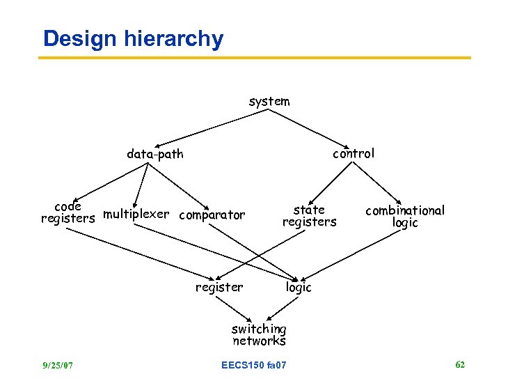 Design hierarchy system control data-path code registers multiplexer comparator register state registers combinational logic switching networks 9/25/07 EECS 150 fa 07 62
 Good luck on the Midterm… 9/25/07 EECS 150 fa 07 63
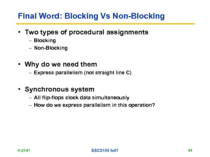 Final Word: Blocking Vs Non-Blocking • Two types of procedural assignments – Blocking – Non-Blocking • Why do we need them – Express parallelism (not straight line C) • Synchronous system – All flip-flops clock data simultaneously – How do we express parallelism in this operation? 9/25/07 EECS 150 fa 07 64
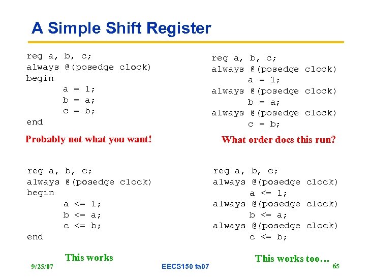 A Simple Shift Register reg a, b, c; always @(posedge clock) begin a = 1; b = a; c = b; end reg a, b, c; always @(posedge clock) a = 1; always @(posedge clock) b = a; always @(posedge clock) c = b; Probably not what you want! What order does this run? reg a, b, c; always @(posedge clock) begin a <= 1; b <= a; c <= b; end 9/25/07 This works reg a, b, c; always @(posedge clock) a <= 1; always @(posedge clock) b <= a; always @(posedge clock) c <= b; EECS 150 fa 07 This works too… 65
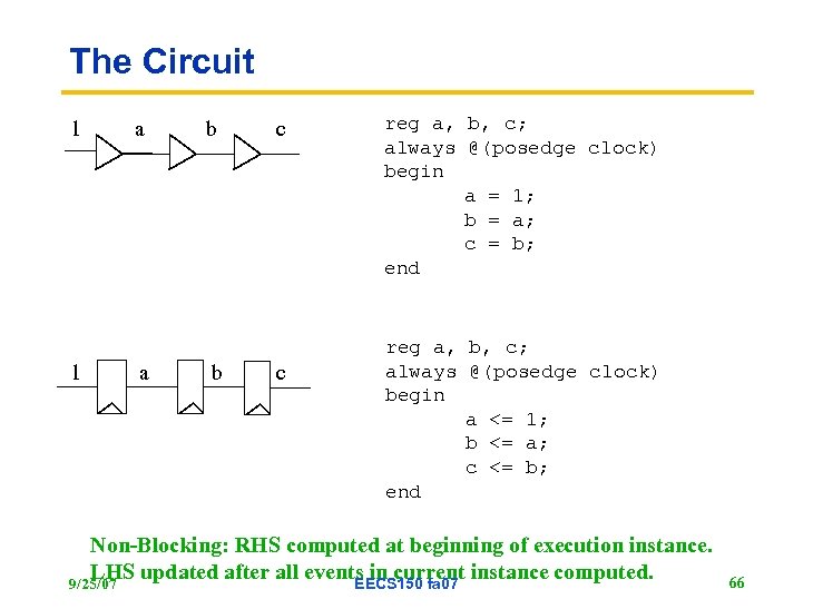 The Circuit 1 1 a a b b c c reg a, b, c; always @(posedge clock) begin a = 1; b = a; c = b; end reg a, b, c; always @(posedge clock) begin a <= 1; b <= a; c <= b; end Non-Blocking: RHS computed at beginning of execution instance. LHS updated after all events in current instance computed. 9/25/07 EECS 150 fa 07 66


