d16b80c26b907a4d0ed63b91f2d3bb1f.ppt
- Количество слайдов: 77


EE 573 VLSI 시스템개론 2004 년도 봄 학기 경 종민

강의 정보 • 목적; 경쟁력 있는 (시스템 개념, know-what 과 시장 을 아는 기술자, 생각하고 질문하고 표현할 줄 아는) So. C 설계자로 전향케 함. • 장소; LG MM-> 창의학습관 201 호(? ) • 조교; 심희준, 김형옥 • Website ; Q&A(조교, 교수), 숙제 및 모든 제출물, 수 강생 개인 사진+소개 자료 제출 요망(1주 내로) (http: //vswww. kaist. ac. kr/course/ee 573/) • Text ; 따로 없음 • Reference ; 추후 통지
 IT Future Trend and Role")
EE 573 강의 내용과 일정 • • (1; 3/3) IT Future Trend and Role of So. C VLSI (1; 3/8) Various So. C-Related Applications, Business Models, Global Industries & Career/Life Planning • (3; 3/10, 15, 17) Key Issues in Embedded System Design (Requirement Generation & HW/SW Co-Design and Co-Verification) • (3; 3/22, 24, 29) High-Speed Design Techniques • (0. 5; 3/31) 45 -min. Test(Mid-term) • (1. 5; 3/31, 4/7) Signal Integrity Issues • (3; 4/12, 14, 19) Infrastructures (Power/Ground & Clocks), Interconnections and Packaging Techniques • (1; 4/21) IP-Based Design Methodology • (1; 4/26) How to present, write, talk, discuss, negotiate and live successful life • (1; 4/28) Testing, Reliability and Manufacturing Issues • (1; 5/3) Reconfigurable Systems Design Techniques • (1; 5/10, 7: 30 am-10: 30 am) Poster Presentation • (2. 5; 5/11, 17, 19) Low-Power Design Techniques • (0. 5; 5/19) 45 -min Test (Final Exam) • (2; 5/24, 6/2) Memory System Design Techniques • (2; 6/14, 6/16, 7: 30 am-10: 30 am) Oral Presentation (15 min. for each person) Total 27 units
 Subject of Learning • (1;")
강의 내용과 일정 • (No. of units ; Date) Subject of Learning • (1; 3/3) IT Future Trend and Role of So. C VLSI • (1; 3/8) Various So. C-Related Applications, Business Models, Global Industries & Career/Life Planning • (3; 3/10, 15, 17) Key Issues in Embedded System Design (Requirement Generation & HW/SW Co-Design and Co. Verification) • (3; 3/22, 24, 29) High-Speed Design Techniques • (0. 5; 3/31) 45 -min. Test(Mid-term) • (1. 5; 3/31, 4/7) Signal Integrity Issues • (3; 4/12, 14, 19) Infrastructures (Power/Ground & Clocks), Interconnections and Packaging Techniques • (1; 4/21) IP-Based Design Methodology
 How to present, write, talk, discuss, negotiate and")
강의 내용과 일정 • (1; 4/26) How to present, write, talk, discuss, negotiate and live successful life • (1; 4/28) Testing, Reliability and Manufacturing Issues • (1; 5/3) Reconfigurable Systems Design Techniques • (1; 5/10, 7: 30 am-10: 30 am) Poster Presentation • (2. 5; 5/11, 17, 19) Low-Power Design Techniques • (0. 5; 5/19) 45 -min Test (Final Exam) • (2; 5/24, 6/2) Memory System Design Techniques • (2; 6/14, 6/16, 7: 30 am-10: 30 am) Oral Presentation (15 min. for each person) • Total 27 units
 출석 ; n 번째")
Grading System • • • Homework ; ~5 pieces (20%) 출석 ; n 번째 결석시 (n-2)% 씩 감점 Midterm ; 15% Final ; 15% Poster(10%) + Presentation(10%) ; 20% • Oral Presentation(15%) + Written Paper (15%) ; 30%
")
IT Future Trend and Role of So. C VLSI 3/3 (#1)

What is So. C? ? • Printed Circuit Board vs. Silicon board P RTL ROM Netlist vs. • Design Reuse Use IP !! • Design Specification Use C Language !! • Verification Methodology In-System Verification !!
 and designer")
Advent of SOC • Growing design productivity gap between gate density (58%/Y) and designer productivity (21%/Y) • Shrinking Time-To-Market (narrow market window) • Viable solution Design Reuse PCS PCs Color TV Cable TV DVB Cellular VCRs Black & White TV DVD 1 million Units 5 International Technology Roadmap For Semiconductors 1999 Ed. - Semiconductor Industry Association 10 15 Wireless Communications Report, BIS, Boston, 1995+ Dataquest 20 years

Evolution of reuse Until early 80’s-90’s Late 90’s – TTL/MSI Reuse of Tr. ASIC/ASSP Reuse of Gates System-on-chip Reuse of Socketized IP Hard component from A company Hard component from B company Virtual component from C company Virtual component from D company

Design methodology & reuse model Plug & play SOC Complex ASIC with a few IPs u. P Core ASIC on DSM Area Driven Timing-driven design (TDD) Personal Reuse Designerspecific reuse practices Retaining key personnel Source Reuse Functional starting points for block design Document, testbench, predictability Opportunistic IP Reuse FIFO SRAM Block-based design (BBD) USB MPEG SW I/F IP FLASH D-Cache SRAM FLASH Logic SRAM u. P Core Logic Platform-based design (PBD) Core Reuse Virtual Component Reuse Predictable, Pre-verified, Core function Socketized Functions for Plug & Play integration Firm/hard IP Planned IP Reuse Adopted from ‘Surviving the SOC revolution’ by H. Chang et. al.

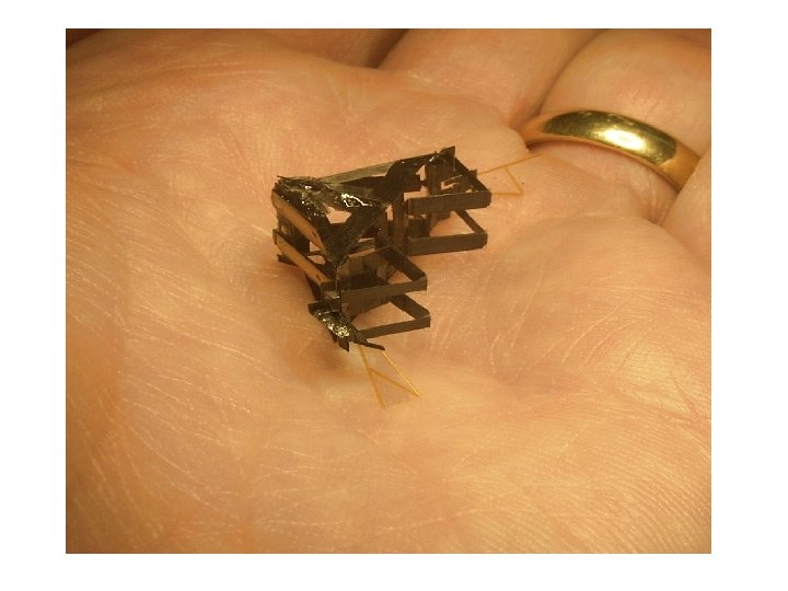
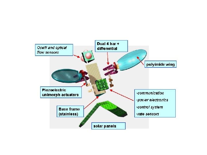
Mote

Artist's conception of future MFI with optical flow sensors and radio. (Quan Gan, UC Berkeley, March 2004)
; Read the following thesis and comment.")
• Homework #1 (Smart Dust by Pister); Read the following thesis and comment. (due 2 weeks; 3/17 class) • http: //wwwbsac. eecs. berkeley. edu/archive/users /hollarseth/publications/cotsdust. pdf
")
Composition of TWG (2003)
 2002. 9. 9")
Future Prospect of IC Technology (ITRS) 2002. 9. 9

Contents • Introduction – ITRS • Overall Roadmap – – – Product Generation Lithography Package Power Cost • Design Technology Challenges – Introduction – Complexity, Methodology – Design Technology Challenges

ITRS Introduction • ITRS International Technology Roadmap for Semiconductors 1992 NTRS 1994 NTRS 1997 NTRS 1998 Update 2000 1999 update ITRS 2001 ITRS SIA – Predicts the main trends in the semiconductor industry – Provides a reference of requirements, potential solutions, and their timing for the semiconductor industry – ITWG (International Technology Working Group) http: //public. itrs. net
 – System Driver • Focus")
ITWG • Overall Cordination – ORTC(Overall Roadmap Technology Characteristic) – System Driver • Focus ITWGs – – – – Design Test Process Integration, Device, and Structures Front End Process Lithography Interconnection Factory Integration Assembly and Packaging • Crosscut ITWGs – – Environment, Safety, and health Yield Enhancement Metrology Modeling and Simulation

Prediction Classification • Red Brick Wall – There are no “known manufacturable solution” to continued scaling – Historical trends of progress might end if some real breakthroughs are not achieved in the future • Yellow: defined as “manufacturable solutions are known” • White: defined as manufacturable solution are known and are being optimized
 – Reports Improvement Trends • Integration Level (Moore’s Law), Cost,")
ITRS 2001 • ITRS(2001) – Reports Improvement Trends • Integration Level (Moore’s Law), Cost, Speed, Power, Compactness, Functionality – Provides 15 -years outlook on the major trends Each technology written by corresponding ITWG Composition of the ITWG (International Technology Working Group) < By Regions > < By Affiliations >

ITRS 2001 < Production Ramp-up Model and Technology Node > “Production” time (year of production) • When the first company brings a technology to production and a second company follows within three months

Product Generation • Product Generations & Chip-Size Model – DRAM (Historically recognized as the technology drivers for the entire semiconductor industry) • Minimization of the area occupied by the memory cell • Maximization of the capacitance for charge storage – MPU/ASIC • Length of the transistor gate • Number of interconnect layers • Metal half-pitch will trail slightly behind or equal to the DRAM half-pitch – DRAM and microprocessor products will share the technology leadership role

Product Generation • Product Generations & Chip-Size Model

Product Generation • Product Generations & Chip-Size Model
 – Enhance equipment productivity")
Lithography • To maintain historical trend (Reducing cost/function by 25~30%/year) – Enhance equipment productivity – Increase manufacturing yields – Use the largest wafer size available – Increase the number of chips available on a wafer

Package • Number of Pads and Pins – Increase number of I/O signals • For higher number of functions on a single chip – Additional power and ground connections To optimize power management To increase noise immunity • MPU (1: 2 = I/O : power/ground) – Two power/ground pads for every signal I/O pad • ASIC (1: 1) – One power/ground pad for every signal I/O pad

Package • Number of Pads and Pins

Package • Pin count/Cost-per-pin # of package pin/balls increases at 10%/year Cost/pin decreases at 5%/year Average cost of packaging will increase at 5%/years – To reduce the overall system pin requirements • Combining functionality into SOC • Multi-chip modules • Bumped chip-on-board

Package • Pin count/Cost-per-pin

Package • Electrical Signals Instructions/second doubles every 1. 5~2 years Increase Processing power – To optimize signal and power distribution • • Increasing # of layers of interconnect Size downscaling of interconnect Using copper(low resistivity) Using inter-metal insulating materials of lower dielectric constant

Power • Reduction of power supply voltage – Reduction of power dissipation – Reduction of transistor channel length – Reduction of reliability of gate dielectrics

Cost • Reducing cost per function by 25~30%/year • Twice the functionality on-chip every 1. 5~2 years

DT Introduction • DT – Enables the conception, implementation, and validation of microelectronics-based systems. – Include tools, libraries, manufacturing process characterization, and methodologies • Area – – – Design Process System-Level Design Logical/Circuit/Physical Design Verification Design Test • Crosscutting Challenges – – – Productivity Power Manufacturing Integration Interference Error-Tolerance

Design Productivity Gap # of available transistors grows faster than the ability to design them meaningfully Investment in process technology has by far dominated investment in design technology – Software now routinely accounts for 80% of embedded systems development cost – Verification engineers are twice as numerous as design engineers on microprocessor project team – Test cost has grown exponentially relative to manufacturing cost

Design Productivity Gap

DT Complexity • Silicon Complexity 1. Non-ideal scaling of device parasitics and supply/threshold voltages • Leakage, power management, circuit/device innovation, current delivery 2. Coupled high-frequency device and interconnect • Noise/interference, signal integrity analysis and management, substrate coupling, delay variation due to cross-coupling 3. Manufacturing equipment • Statistical process modeling, library characterization 4. Scaling of global interconnect performance relative to device performance • Communication, synchronization

DT Complexity 5. Decreased reliability • Gate insulator tunneling and breakdown integrity, joule heating and electromigration, single-event upset, general faulttolerance 6. Complexity of manufacturing handoff • Reticle enhancement and mask writing/inspection flow, NRE cost 7. Process variability • Library characterization, analog and digital circuit performance, error-tolerant design, layout, reuse, reliable and predictable implementation platforms

DT Complexity • System Complexity 1. Reuse • Support for hierarchical design, heterogeneous SOC integration (modeling, simulation, verification, test of component blocks) especially for analog/mixed-signal 2. Verification and test • Specification capture, design for verifiability, verification reuse for heterogeneous SOC, system-level and software verification, verification of analog/mixed-signal and novel devices, self-test, intelligent noise/delay fault testing, tester timing limits, test reuse 3. Cost-driven design optimization • Manufacturing cost modeling and analysis, quality metrics, cooptimization at die-package-system levels, optimization with respect to multiple system objectives such as fault tolerance, testability, etc.

DT Complexity 4. Embedded software design • Predictable platform-based system design methodologies, co -design with hardware and for networked system environments, software verification/analysis 5. Reliable implementation platform • Predictable chip implementation into multiple circuit fabrics, higher-level handoff to implementation 6. Design process management • Design team size and geographic distribution, data management, collaborative design support, “design through system” supply chain management, metrics and continuous process improvement

DT Methodology Precepts • Design Methodology combines – Top-down planning and search (system specification and constraints) with – Bottom-up propagation (physical laws, limits of manufacturing technology/cost)

DT Methodology Precepts • Future Design Methodologies and component tools – Exploit reuse – Evolve rapidly( evolution of suite vectors from simulation to verification, constraints for synthesis and optimization, and test) – Avoid iteration – Replace verification by prevention(ex; lower-level problems, i. e. , crosstalk/delay uncertainty, can be better addressed by upper-level prevention, i. e. , shielding/repeater insertion)

DT Methodology Precepts – Improve predictability – Orthogonalize concerns; divide and conquer, treat separately if possible(computing and communication, behavior and architecture, etc. ) – Expand scope; gather and conquer, treat together if possible(digital and analog, digital HW and software, internal, , operation and human interface, multi-level modelling, simulation) – Unify; synthesis and analysis, logical/physical/timing, design and test.

DT Methodology • Methodology Precepts

Design Technology • DT Area – – – Design Process System-Level Design Logical, Circuit, and Physical Design Verification Design Test

Design Technology
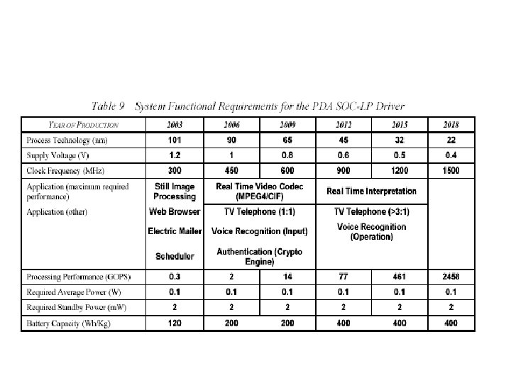
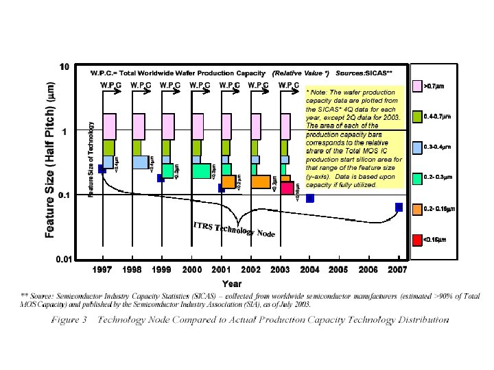
 year 2004 07 10 13 2016 90 65 45 32 22")
ITRS 2003 Roadmap(1) year 2004 07 10 13 2016 90 65 45 32 22 MPU gate length [nm] (printed/physical)** 53/37 35/25 25/18 18/13 13/9 Vdd [V] (high-perf. /low power) 1. 2/0. 9 1. 1/0. 8 1. 0/0. 7 0. 9/0. 6 0. 8/0. 5 Max. power consumption [W] (hi-perf. /cost-perf. /battery) 158/84/ 2. 2 189/104 / 2. 5 218/120 / 2. 8 251/138 / 3. 0 288/158 / 3. 0 DRAM ½ pitch [nm]* * MPU/ASIC metal 1 ½ pitch : DRAM ½ pitch 1. 2 ** Si atom size : ≃ 0. 5 nm
![ITRS 2003 Roadmap(2) Year 04 07 10 13 16 MPU chip size [mm 2]](https://present5.com/presentation/d16b80c26b907a4d0ed63b91f2d3bb1f/image-52.jpg "ITRS 2003 Roadmap(2) Year 04 07 10 13 16 MPU chip size [mm 2]")
ITRS 2003 Roadmap(2) Year 04 07 10 13 16 MPU chip size [mm 2] (intro. /prod. ) 280/ 140 280/ 140 ASIC max. chip size [mm 2] 572 572 572 Litho. Field size [mm] (L/W) 32/22 32/22 Wafer diameter [mm] 300 300 450
 Year 04 07 10 13 16 Total # of pads (MPU)*")
ITRS 2003 Roadmap(3) Year 04 07 10 13 16 Total # of pads (MPU)* 3072 3840 4224 4416 Total # of pads (ASIC)** 3600 4400 4800 5400 6000 Pad pitch [um] (ball/wedgy) 35/25 25/20 20/20 Pad pitch [um] (area flipchip/periphral fc) 150/6 120/3 100/2 90/20 80/15 0 0 0 * ⅓ for signal I/O, ⅔ for PWR/GND ** ½ for signal I/O, ½ for PWR/GND
![ITRS 2003 Roadmap(4) Year 04 07 10 13 16 Clock frequency [MHz] (on-chip clock/chip-toboard)](https://present5.com/presentation/d16b80c26b907a4d0ed63b91f2d3bb1f/image-54.jpg "ITRS 2003 Roadmap(4) Year 04 07 10 13 16 Clock frequency [MHz] (on-chip clock/chip-toboard)")
ITRS 2003 Roadmap(4) Year 04 07 10 13 16 Clock frequency [MHz] (on-chip clock/chip-toboard) 4171/ 2500 9285/ 4883 15079 / 9536 22980 / 18626 39683 / 36379 Max. # of wiring levels (Max. /Min. ) 14/10 15/11 16/12 18/14 # of mask levels (MPU/DRAM) 31/24 33/24 35/26 39/26

Near-term Breakthroughs in Design Technology for AMS
: IT의 역할과 비중 정보(Information)/지식(Knowledge)의 가치, 역할 : Last frontier after mass,")
1. %(IT/So. C): IT의 역할과 비중 정보(Information)/지식(Knowledge)의 가치, 역할 : Last frontier after mass, wave and energy ! IT(information) 반도체 software Wireless & Wired comm. link Wave Current duality Mass E = MC 2 Energy
대 공신 : (전기+반도체+software)+wireless 통신기술 정보의 저장과 처리 반도체 software 전류 (current) 정보의")
IT의 3(+1)대 공신 : (전기+반도체+software)+wireless 통신기술 정보의 저장과 처리 반도체 software 전류 (current) 정보의 전달 + Wireless/ Wired 통신기술 전파 (wave)
,")
IT: 정보의 {표현, 변형, 저장, 전송}을 위한 methodology; • Medium(반도체, fiber, free space, molecule), mechanism(motor, 트랜지스터, …)과 information carrier(전자, photon, E/M wave, …)은 다양하며 변한다. 예) VLSI photonics MEMS Bio carrier electron photon micro-muscle radical mechanism transistor lens E/M-force atomic force medium semiconductor fiber/free space semi-substrate Molecule
 IT 기술분야 overview • 정보의 생성/도출 – HW : 각종 sensor(압력, 가스, 속도)")
7) IT 기술분야 overview • 정보의 생성/도출 – HW : 각종 sensor(압력, 가스, 속도) – System : 디지털/TV 카메라, 기상 satellite, 전자칠판, 계측장비 • 정보의 변환 – HW : 각종 transducer, A/D-D/A 변환기, rf 변환기, serdes, codec – SW : compiler, assembler, 자연어 번역
, FPGA, ASIC, PC,")
• 정보의 처리 – HW : software platform(microprocessor, microcontroller, DSP), FPGA, ASIC, PC, Computing Server – SW : cryptography, authentication, 영상/음성 변복 조 및 압축 CDMA, 채널 코딩 및 변복조, 에러 코딩 및 복원, motion estimation, e-commerce, RTOS, 음성/ 영상 인식, EDA tools, 3 -D graphics, animation, spreadsheet – System : PC, NMR, 초음파진단기, PDA, GPS, cellular phone

• 정보의 저장 – HW : HDD, CD-ROM, MOD, DVD, SDRAM, FRAM, MRAM, Flash, tape – SW : 데이터웨어 하우징, DBMS – System : RAID, Smart card

• 정보의 전달 – HW : fiber optics, switch, laser diode, antenna, Ir. DA – SW : TCP/IP, MPLS, ATM/ethernet protocol, MAC protocol, IPv 6, TP monitor – System : router, repeater, NIC, home. PNA, bluetooth • 정보의 소비 – HW : 브라운관, LCD, PDP, EL display, speaker, printer head – System : micro-robot, TV, laser/ink-jet printer, motor, CNC machine

IT vs. 타기술/응용분야 응용 기술분야 의 료 의 약 IT BT 교 통 문화/ 환 국방 오락 식료 경 (warfare) (ET) (CT) NT 통 신 우주 항공 제조기술 에너지기술

세계의 IT 산업/기술현황 • 미국 – 최대 IT 생산국이자 소비국 – IBM, Intel, Lucent, HP, Motorola, TI, SUN, Cisco, SGI, Broadcom 등 반도체, hardware 및 system 업체, Microsoft, Oracle 등 software 업체, Yahoo, Netscape 등 internet 업체 등 세계 굴지의 업체 포진 – Stanford, MIT, Berkeley 등 일류대학에 전세계의 인재 들 모여들어 활동

– 기술발전 Roadmap, 각종 Standard, Consortium 구성 에 정부와 민간의 주도적 역할 – 활발한 기업간 M&A로 빠른 발전/변화 – Software와 System 산업 위주이며, 각종 standard 주 도와 royalty에 의한 수입 비중이 큼 – BT와 NT 등에도 압도적인 우위를 점령할 것으로 예상 됨

– 인터넷, software, 시스템 설계 등 통신 및 컴퓨팅 분야 의 첨단 IT 기술의 선점을 통하여 1970년대부터 본격 시작된 가전분야의 제조업 중심의 일본의 추격을 1990 년경에 성공적으로 따돌리게 됨 – 우주개발 단독선두, MD 등 군수산업이 IT 기술의 booster 역할 겸 국가의 수입원이 됨 – 인도, 대만, 중국, 베트남 등의 우수 인력의 지속적 공급

• 일본 – 기술개량, 기술품질유지, 제조기술에 뛰어난 역량 이 있는 나라 – 자동차, 중장비와 전자산업으로 일어섰으나, 반도 체 산업 중 메모리에서 한국에 10년전에 추월당했 고, PC의 자국 표준 고집으로 자충수에 빠지게 됨
로 인해 성능과")
– 대기업 중심의 기계적인 문화(합의 시너지는 있으나, 곱 의 시너지는 없는 문화)로 인해 성능과 안정성보다 창의 성과 inter-operability가 요구되는 소프트웨어나 시스 템 설계 분야에서 뒤쳐짐. 안정된 부품 업체는 있으나, 창의적 벤처기업은 적다. – 미국에 비해 기반기술이 뒤쳐짐을 각성하고 약 10여년 전부터 새 기술 분야의 기초연구에 적극투자 하기 시작

• 독일 – Infineon, Mercedes, BMW, Bosch, AEG, Siemens 등 굴지의 기업과 Fraunhofer, Max Planck 연구소 등 건재 – 벤처기업 활동 최근 왕성 – 의용, 자동차, 정밀, 공작기 관련 전자기술에서 선 도적 위치

• 영국 – 정부주도의 강력한 IT 기술 드라이브 – ARM사의 microprocessor core 사업은 탁월한 성공 모델 – software, marketing, 보험, financing 분야의 선도 • 벨기에 – 1984년 설립된 IMEC의 눈부신 역할 : 현재 연 100 M 유로의 수탁연구, 수많은 우수한 연구, 창업산파역
, 순수과학은 Weizmann Institute로 대별된")
• 이스라엘 – 엔지니어링은 Technion(이스라엘 고급 기술인력의 70% 공급), 순수과학은 Weizmann Institute로 대별된 다. – 미국 Nasdaq 상장기업이 77개(미국에서 창업 상장한 것 포함시 120여개)로 2위의 캐나다(126개)에 이어 3 위 – 전세계의 유수기업(Intel, IBM, Motorola 등)의 연구소 가 모두 Technion 공대가 있는 갈멜산 자락에 입주. (특 히, Intel의 경우 processor의 핵심구조와 software 설 계는 이스라엘에서 함. )
보다 크게 앞섬 – 소프트웨어, 방위산업,")
– 기술자 수가 인구 10, 000명당 135명으로 2위의 미국(85명)보다 크게 앞섬 – 소프트웨어, 방위산업, 무선통신, 인식 및 추적기 술이 선도적 – BT에 과감한 투자 이미 시작(Weizmann이 매우 강한 분야, 이스라엘 과학자의 35%가 BT 종사, 총 연구비의 40%가 BT에 쓰임)

• 대만 – 1973년 도 에 설 립 된 ITRI(Industrial Technology Research Institute : 공업기술연구원)이 국가산업을 일으키는데 결정적 역할 – ERSO(Electronics Research & Service Organization)은 그중의 전자파트로서 UMC, TSMC와 같은 큰 기업의 모체가 되었음
이 1980년에 만들어져 대만")
– 신 죽 에 위 치 한 HSIP(Hsinchu Science-based Industrial Park)이 1980년에 만들어져 대만 3大 명문이며 이공계 위주 대학인 단지내의 청화대, 교통대의 인력을 기반으로 반도체· 전자산업 중심으로 급속 성장. 우리나라의 구미공단과 대덕 과학단지보다 후발이나, 두가지의 중간개념으로 시작한 것 이 성공요인. 대 만 ITRI • • 1973년 설립 기업관련 연구위주 의도적인 기업 spin-off 정책 고위경영 경험있는 과학기술자들 HSIP 한 국 기업과 연구소, 대학의 공존 ·협력 KIST • • 1965년 설립 순수연구 + 약간의 용역 연구 수준 전문연구소와 경쟁입장 산연협동·경영경험 부족 대덕과학단지 고립된 과학기술연구, 단지내 교류 부족 구미 공단 수출위주의 조립 공업

• 스웨덴 – 스톡홀름에서 20분 거리에 Wireless Valley의 KISTA Science Park : 700여개 정보통신 업체(Ericsson, IBM, 인텔, 선, 컴팩, HP, Nortel 등)의 140여 국적의 3만명 고급기술 인력 고용 – Wireless Valley는 Silicon Valley에 이어 제 2위 수준 의 전세계 신경계와 정보통신 중심지 : 이동통신을 비 롯, 통신분야에서 세계 최고의 경쟁력(핵심기술 : 비 동 기 식 W-CDMA, Bluetooth, Optical Switching, DNA computing 등)

– Ericsson : 이동통신 세계 시장 점유율 40%로 1위 – Sweden은 미국 다음으로 높은 GDP 대비 연구투자 비 율(GDP의 3. 8%) – 국내 총생산대비 정보통신·이동통신 투자비율 : 스웨덴 1위(7. 72%), 미국 2위(7. 29%), 영국 3위, 핀랜드 4위 – KISTA 파크의 중심에 RIT(왕립공과대학)의 IT campus 와 스톡홀름 공대가 강의실이 있다. 산·학·연 복합 교육
 ; Architecture/algorithm 설계 시스템설계 HW/SW 동시설계(simulation, 검증) 디지털 엔지니어,")
So. C comes from(needed expertise) ; Architecture/algorithm 설계 시스템설계 HW/SW 동시설계(simulation, 검증) 디지털 엔지니어, 소프트웨어 엔지니어 Logic 설계/analog block 설계 SW 프로그래밍(응용, OS, firmware), -programming 기능 Speed Cost 만족 회로 설계 Physics (전자기, 열, 전력…) 기본 cell(memory, logic, …) 및 low-level 회로 설계 Signal integrity, radiation/sensitivity, skew, power 소모, yield 해석 검사
d16b80c26b907a4d0ed63b91f2d3bb1f.ppt