021faba54bf5483ea601b523b13d2544.ppt
- Количество слайдов: 47
 EE 4271 VLSI Design Dr. Shiyan Hu Office: EERC 731 Manufacturing Process Adapted and modified from Digital Integrated Circuits: A Design Perspective by Jan M. Rabaey, Anantha Chandrakasan, and Borivoje Nikolic. © EE 141 Integrated Digital Circuits 2 nd 1 Manufacturing
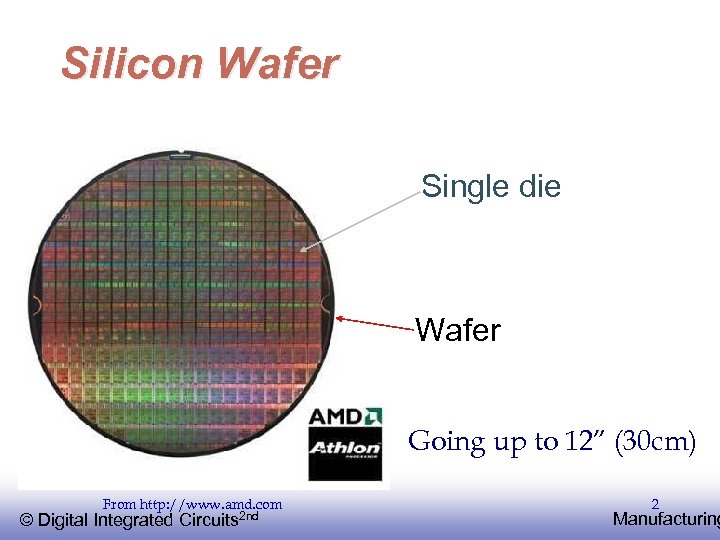 Silicon Wafer Single die Wafer Going up to 12” (30 cm) From http: //www. amd. com © EE 141 Integrated Digital Circuits 2 nd 2 Manufacturing
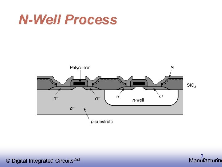 N-Well Process © EE 141 Integrated Digital Circuits 2 nd 3 Manufacturing
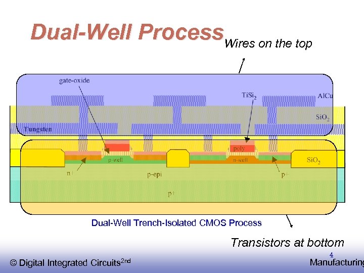 Dual-Well Process. Wires on the top Dual-Well Trench-Isolated CMOS Process Transistors at bottom © EE 141 Integrated Digital Circuits 2 nd 4 Manufacturing
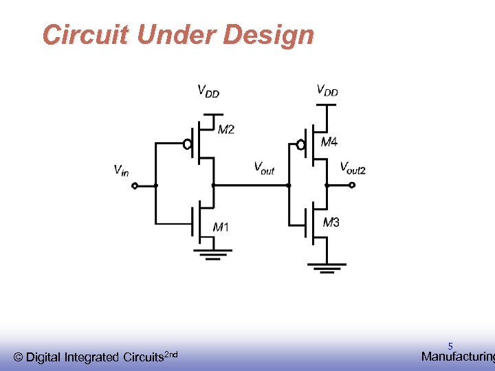 Circuit Under Design © EE 141 Integrated Digital Circuits 2 nd 5 Manufacturing
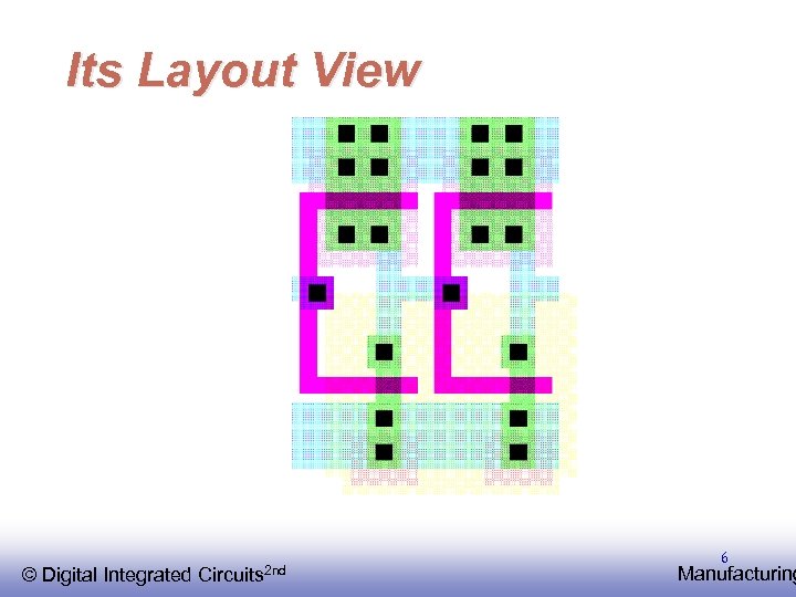 Its Layout View © EE 141 Integrated Digital Circuits 2 nd 6 Manufacturing
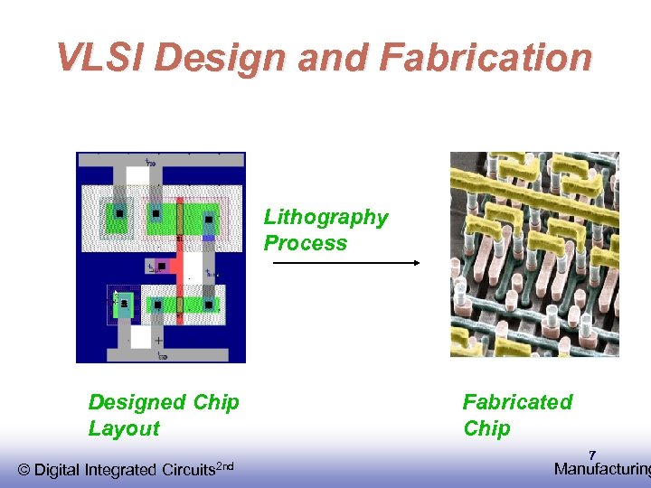 VLSI Design and Fabrication Lithography Process Designed Chip Layout © EE 141 Integrated Digital Circuits 2 nd Fabricated Chip 7 Manufacturing
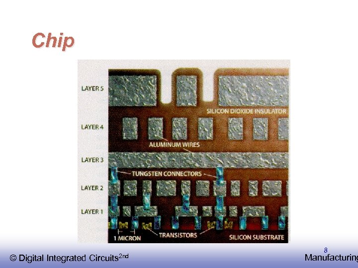 Chip © EE 141 Integrated Digital Circuits 2 nd 8 Manufacturing
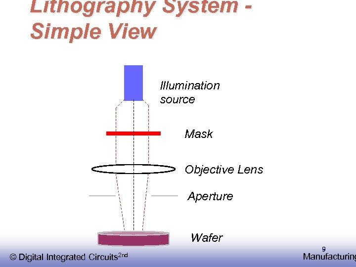 Lithography System Simple View Illumination source Mask Objective Lens Aperture Wafer © EE 141 Integrated Digital Circuits 2 nd 9 Manufacturing
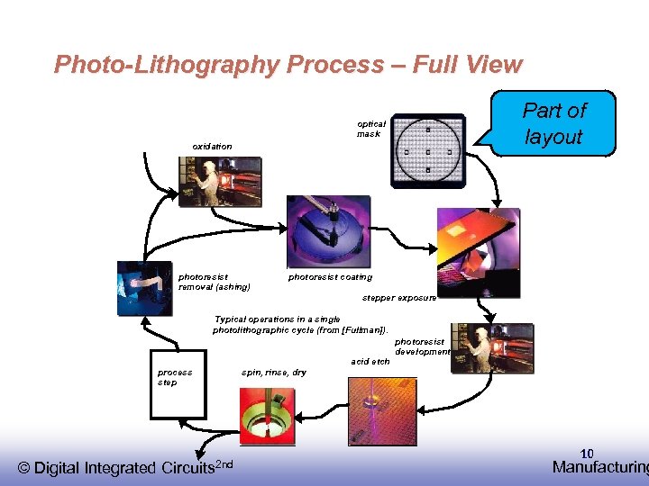 Photo-Lithography Process – Full View Part of layout optical mask oxidation photoresist removal (ashing) photoresist coating stepper exposure Typical operations in a single photolithographic cycle (from [Fullman]). photoresist development acid etch process step © EE 141 Integrated Digital Circuits 2 nd spin, rinse, dry 10 10 Manufacturing
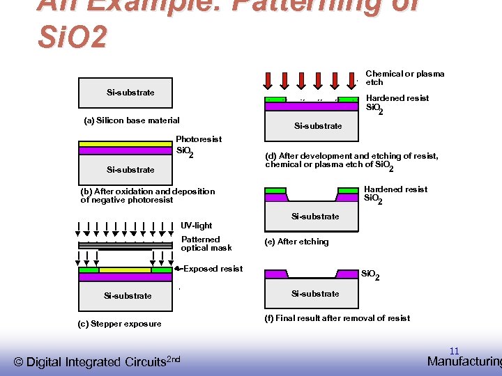 An Example: Patterning of Si. O 2 Chemical or plasma etch Si-substrate Hardened resist Si. O 2 (a) Silicon base material Si-substrate Photoresist Si. O 2 Si-substrate (d) After development and etching of resist, chemical or plasma etch of Si. O 2 Hardened resist Si. O 2 (b) After oxidation and deposition of negative photoresist UV-light Patterned optical mask Si-substrate (e) After etching Exposed resist Si-substrate (c) Stepper exposure © EE 141 Integrated Digital Circuits 2 nd Si. O 2 Si-substrate (f) Final result after removal of resist 11 Manufacturing
 Manufacturing Process Part of the layout is put on a mask (level), so we have many masks. q Each mask level corresponds to different actions in the fabrication process q Each mask level contains non-overlapping polygons, but polygons from different masks may overlap subject to max/min distance rules q Minimum geometry (lambda) rule is used. The overlap is defined using lambda rule. q © EE 141 Integrated Digital Circuits 2 nd 12 Manufacturing
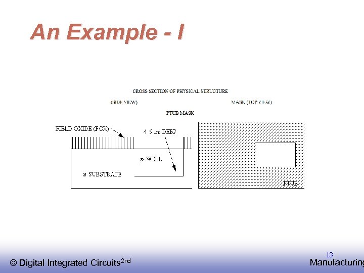 An Example - I © EE 141 Integrated Digital Circuits 2 nd 13 Manufacturing
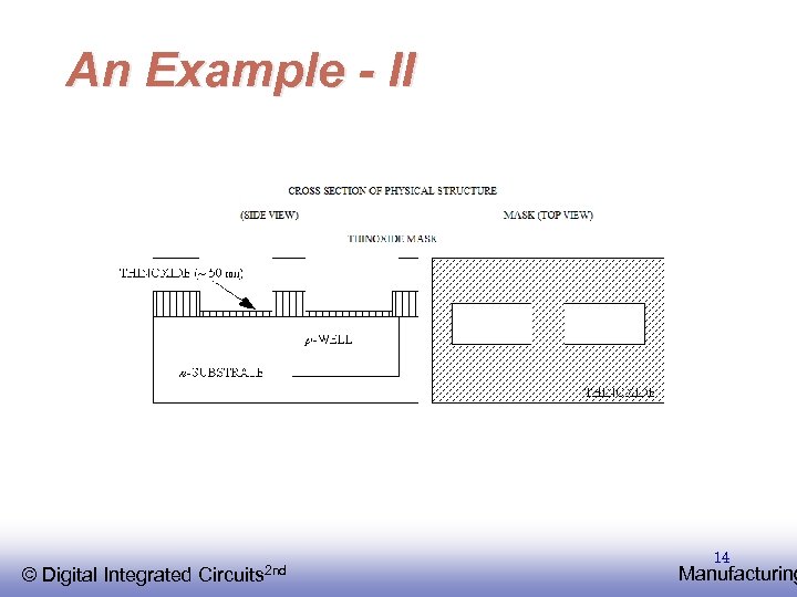 An Example - II © EE 141 Integrated Digital Circuits 2 nd 14 Manufacturing
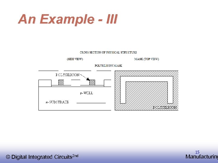 An Example - III © EE 141 Integrated Digital Circuits 2 nd 15 Manufacturing
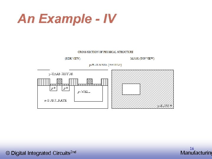 An Example - IV © EE 141 Integrated Digital Circuits 2 nd 16 Manufacturing
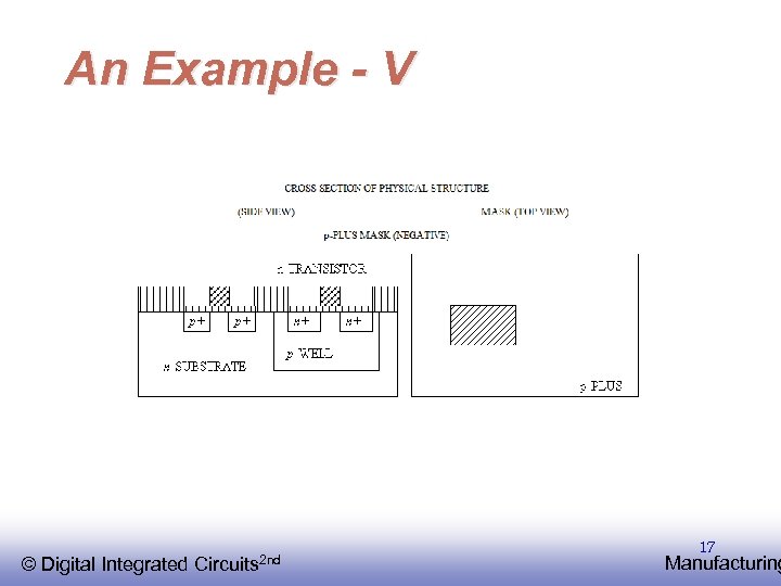 An Example - V © EE 141 Integrated Digital Circuits 2 nd 17 Manufacturing
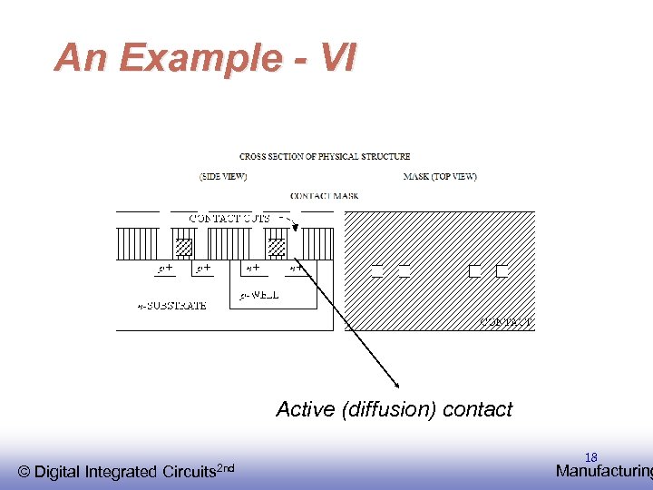 An Example - VI Active (diffusion) contact © EE 141 Integrated Digital Circuits 2 nd 18 Manufacturing
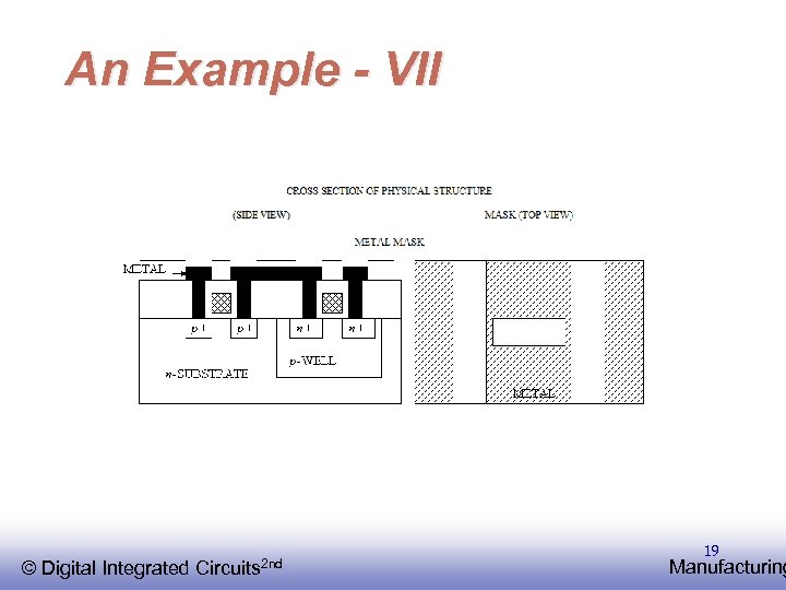 An Example - VII © EE 141 Integrated Digital Circuits 2 nd 19 Manufacturing
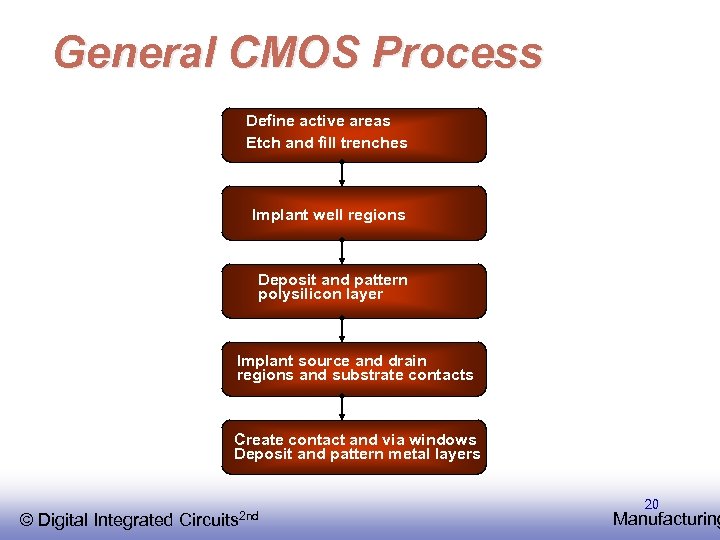 General CMOS Process Define active areas Etch and fill trenches Implant well regions Deposit and pattern polysilicon layer Implant source and drain regions and substrate contacts Create contact and via windows Deposit and pattern metal layers © EE 141 Integrated Digital Circuits 2 nd 20 Manufacturing
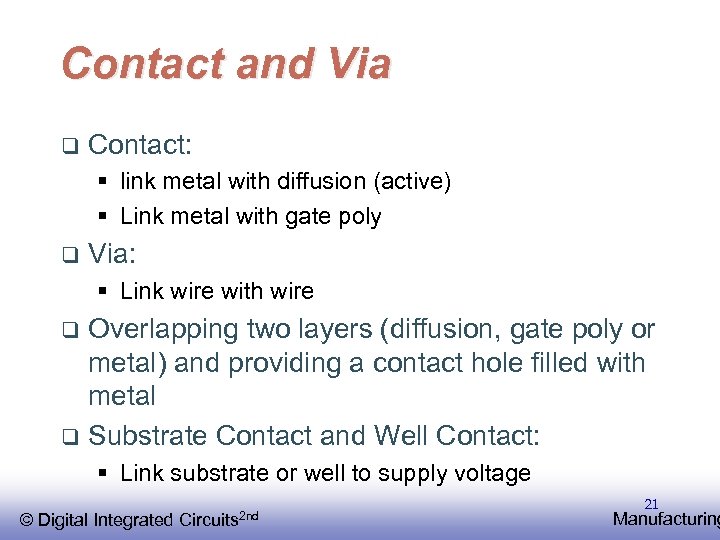 Contact and Via q Contact: § link metal with diffusion (active) § Link metal with gate poly q Via: § Link wire with wire Overlapping two layers (diffusion, gate poly or metal) and providing a contact hole filled with metal q Substrate Contact and Well Contact: q § Link substrate or well to supply voltage © EE 141 Integrated Digital Circuits 2 nd 21 Manufacturing
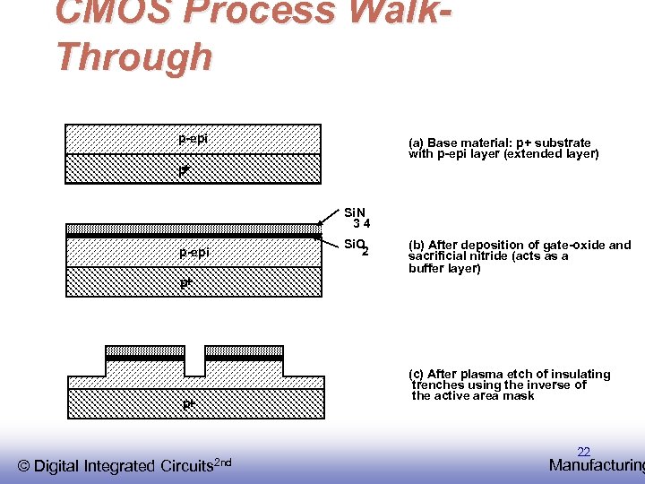 CMOS Process Walk. Through p-epi (a) Base material: p+ substrate with p-epi layer (extended layer) + p Si. N 34 p-epi + p p+ © EE 141 Integrated Digital Circuits 2 nd Si. O 2 (b) After deposition of gate-oxide and sacrificial nitride (acts as a buffer layer) (c) After plasma etch of insulating trenches using the inverse of the active area mask 22 Manufacturing
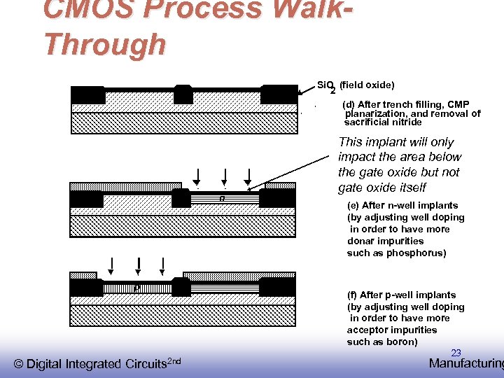 CMOS Process Walk. Through Si. O (field oxide) 2 (d) After trench filling, CMP planarization, and removal of sacrificial nitride n p © EE 141 Integrated Circuits 2 nd Digital This implant will only impact the area below the gate oxide but not gate oxide itself (e) After n-well implants (by adjusting well doping in order to have more donar impurities such as phosphorus) (f) After p-well implants (by adjusting well doping in order to have more acceptor impurities such as boron) 23 Manufacturing
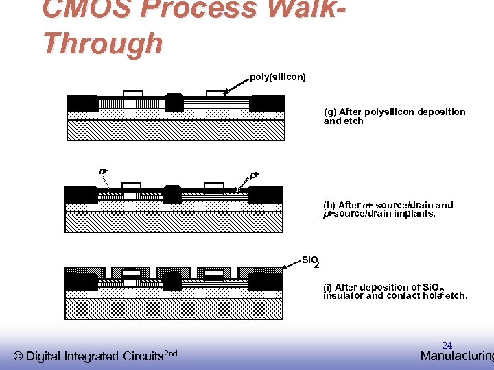 CMOS Process Walk. Through poly(silicon) (g) After polysilicon deposition and etch n + + p (h) After n+ source/drain and p+ source/drain implants. Si. O 2 (i) After deposition of Si. O 2 insulator and contact hole etch. © EE 141 Integrated Digital Circuits 2 nd 24 Manufacturing
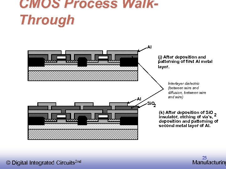 CMOS Process Walk. Through Al (j) After deposition and patterning of first Al metal layer. Al Interlayer dielectric (between wire and diffusion, between wire and wire) Si. O 2 (k) After deposition of Si. O insulator, etching of via’s, 2 deposition and patterning of second metal layer of Al. © EE 141 Integrated Digital Circuits 2 nd 25 Manufacturing
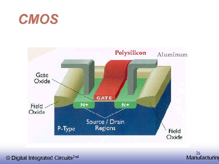 CMOS Polysilicon © EE 141 Integrated Digital Circuits 2 nd Aluminum 26 Manufacturing
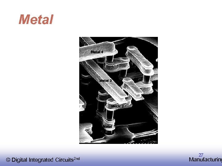 Metal © EE 141 Integrated Digital Circuits 2 nd 27 Manufacturing
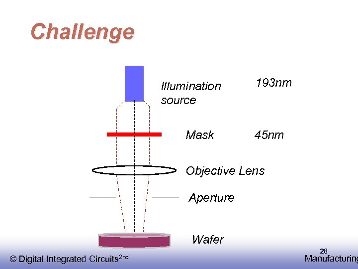 Challenge Illumination source Mask 193 nm 45 nm Objective Lens Aperture Wafer © EE 141 Integrated Digital Circuits 2 nd 28 28 Manufacturing
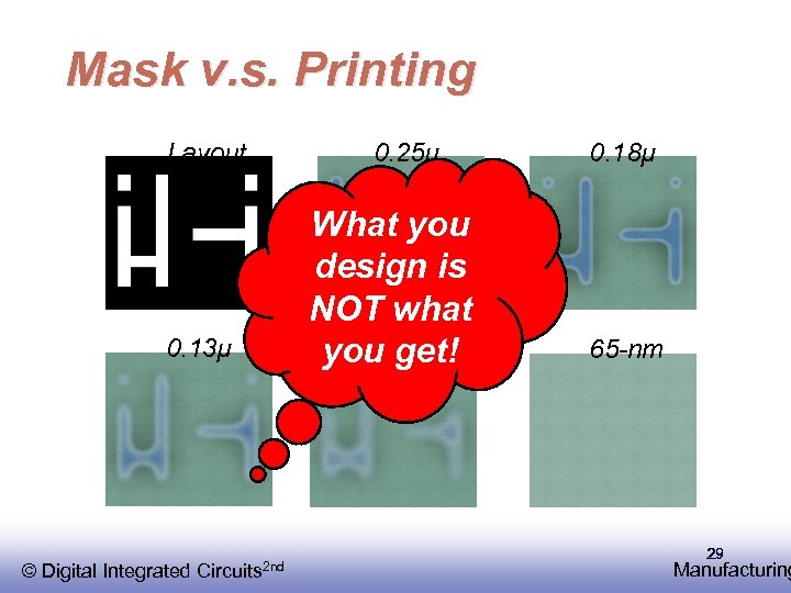 Mask v. s. Printing Layout 0. 13µ © EE 141 Integrated Digital Circuits 2 nd 0. 25µ What you design is NOT what 90 -nm you get! 0. 18µ 65 -nm 29 29 Manufacturing
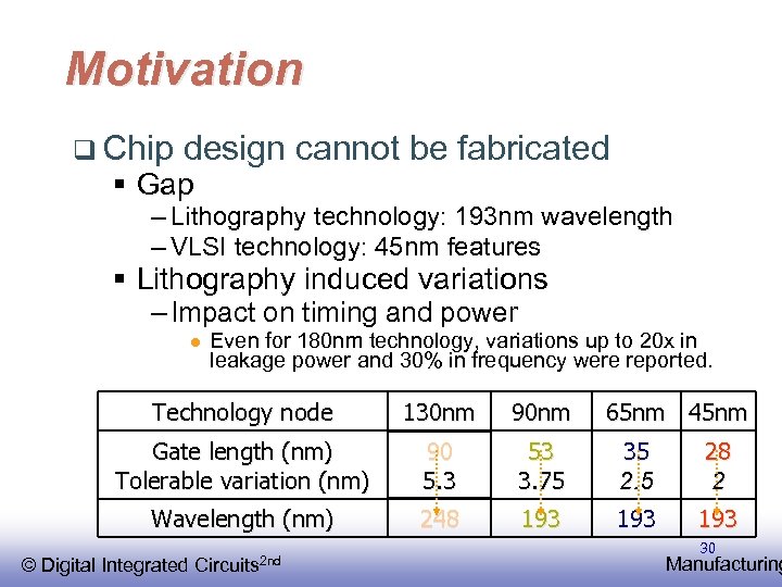 Motivation q Chip design cannot be fabricated § Gap – Lithography technology: 193 nm wavelength – VLSI technology: 45 nm features § Lithography induced variations – Impact on timing and power l Even for 180 nm technology, variations up to 20 x in leakage power and 30% in frequency were reported. Technology node 130 nm 90 nm Gate length (nm) Tolerable variation (nm) 90 5. 3 53 3. 75 35 2. 5 28 2 Wavelength (nm) 248 193 193 © EE 141 Integrated Digital Circuits 2 nd 65 nm 45 nm 30 Manufacturing
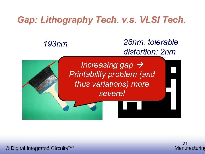 Gap: Lithography Tech. v. s. VLSI Tech. 28 nm, tolerable distortion: 2 nm 193 nm Increasing gap Printability problem (and thus variations) more severe! © EE 141 Integrated Digital Circuits 2 nd 31 31 Manufacturing
 Design Rules © EE 141 Integrated Digital Circuits 2 nd 32 Manufacturing
 Design Rules Interface between designer and process engineer q Guidelines for constructing process masks q Unit dimension: Minimum line width § scalable design rules: lambda parameter § absolute dimensions (micron rules) q © EE 141 Integrated Digital Circuits 2 nd 33 Manufacturing
 Lambda Rule q q Every distance in layout rules is specified by lambda Given a process, lambda is set to a specific value. § Process technology is defined using minimum line width. 0. 25 um technology means minimum line width is 0. 25 um. Lambda=minimum line width/2. § For a 0. 25 um process, lambda=0. 125 um In practice, scaling is often not linear, e. g. , from technology A to B, minimum line width shrink by 0. 5, but it does not necessarily mean that minimum poly-diffusion distance also shrinks by 0. 5. Industry usually uses micron rule and lambda rule is used only for prediction/estimation of the impact of technology scaling to a design. © EE 141 Integrated Digital Circuits 2 nd 34 Manufacturing
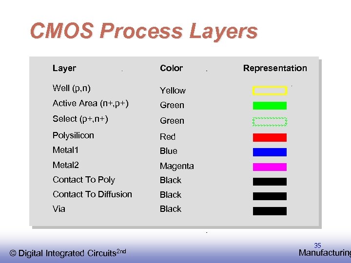 CMOS Process Layer Color Well (p, n) Yellow Active Area (n+, p+) Green Select (p+, n+) Green Polysilicon Red Metal 1 Blue Metal 2 Magenta Contact To Poly Black Contact To Diffusion Black Via Black © EE 141 Integrated Digital Circuits 2 nd Representation 35 Manufacturing
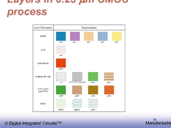 Layers in 0. 25 mm CMOS process © EE 141 Integrated Digital Circuits 2 nd 36 Manufacturing
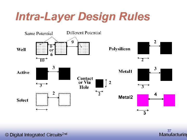 Intra-Layer Design Rules 4 Metal 2 3 © EE 141 Integrated Digital Circuits 2 nd 37 Manufacturing
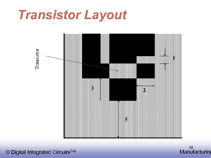 Transistor Layout © EE 141 Integrated Digital Circuits 2 nd 38 Manufacturing
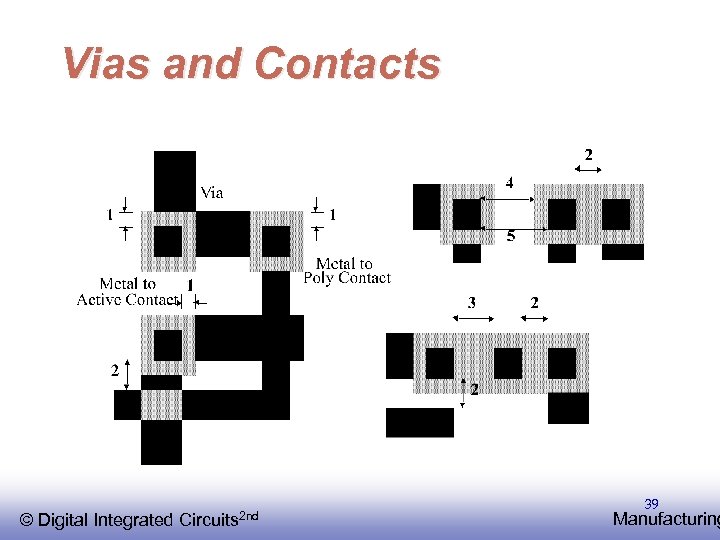 Vias and Contacts © EE 141 Integrated Digital Circuits 2 nd 39 Manufacturing
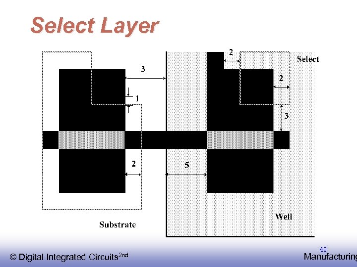 Select Layer © EE 141 Integrated Digital Circuits 2 nd 40 Manufacturing
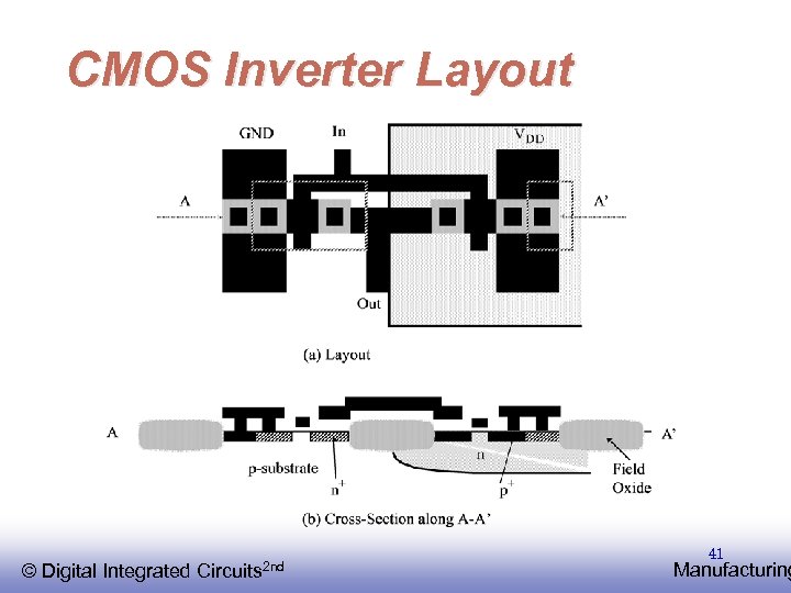 CMOS Inverter Layout © EE 141 Integrated Digital Circuits 2 nd 41 Manufacturing
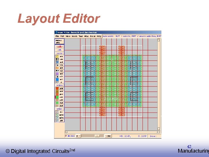 Layout Editor © EE 141 Integrated Digital Circuits 2 nd 42 Manufacturing
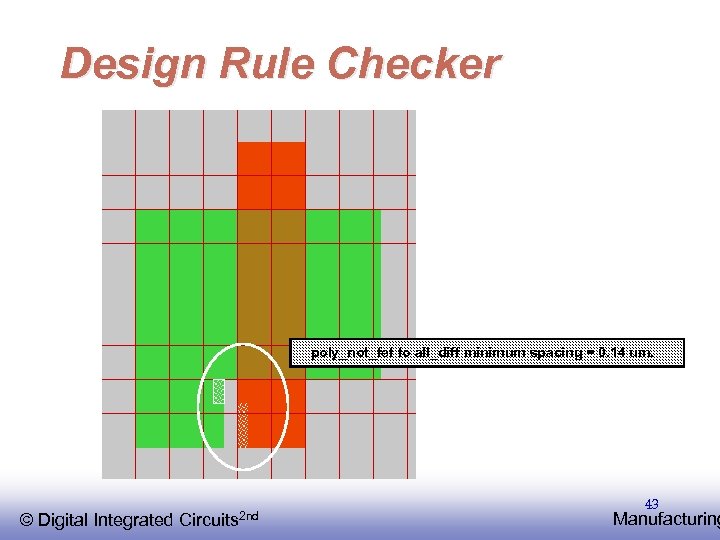 Design Rule Checker poly_not_fet to all_diff minimum spacing = 0. 14 um. © EE 141 Integrated Digital Circuits 2 nd 43 Manufacturing
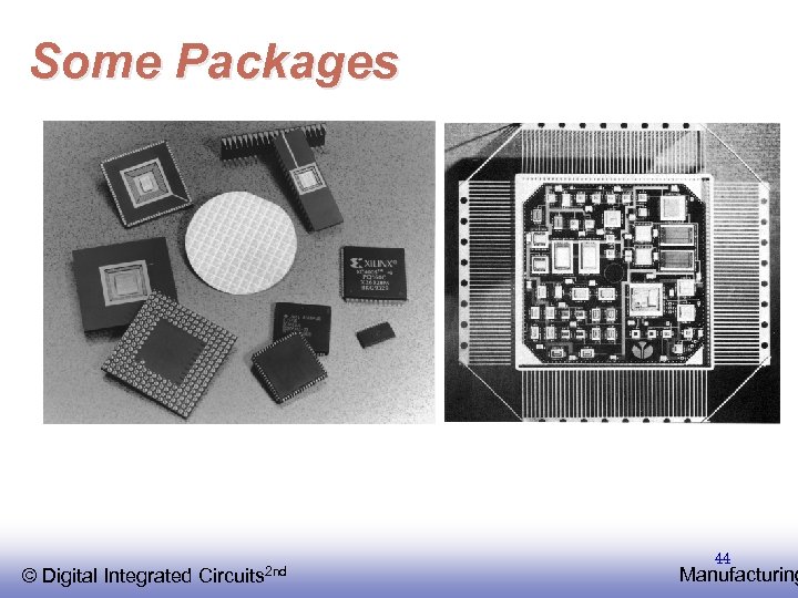 Some Packages © EE 141 Integrated Digital Circuits 2 nd 44 Manufacturing
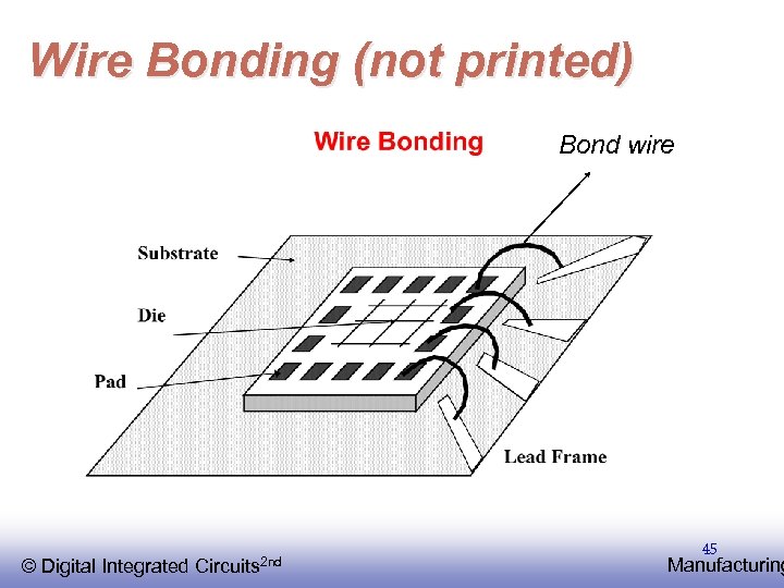 Wire Bonding (not printed) Bond wire © EE 141 Integrated Digital Circuits 2 nd 45 Manufacturing
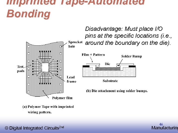 Imprinted Tape-Automated Bonding Disadvantage: Must place I/O pins at the specific locations (i. e. , around the boundary on the die). © EE 141 Integrated Digital Circuits 2 nd 46 Manufacturing
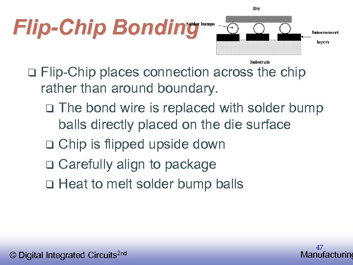 Flip-Chip Bonding q Flip-Chip places connection across the chip rather than around boundary. q The bond wire is replaced with solder bump balls directly placed on the die surface q Chip is flipped upside down q Carefully align to package q Heat to melt solder bump balls © EE 141 Integrated Digital Circuits 2 nd 47 Manufacturing


