e922a5fbc862946786c3f94fac5d9069.ppt
- Количество слайдов: 194
 EE 318 595 Capstone Design Project Spring 2005 Team #3 1 1
 Team #3: Staff • • • Nole Martin Paul Simons Eric Ritzke Tom Reuter Steven Krol Murtadha B. Tunis • • • BSEE BSEE 2
 Team #3: Total Resources • 1200 Man hours • $1000 for material and prototyping • Based on our individual experiences and knowledge our team will strive to exceed all project expectations. 3
 Selected Product • Wireless Weather Buoy • Primary Benefit: Real time Local Weather Information • Intended for use by private water front property owners. • Product will report air and water temperature, barometric pressure and wind speed via RF communications. • Similar weather stations exist, but not for private use. • Maritime Consumer Market 4
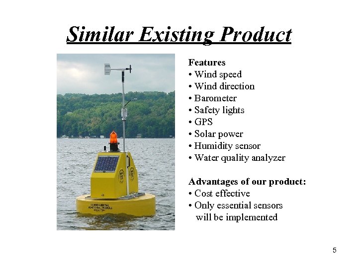 Similar Existing Product Features • Wind speed • Wind direction • Barometer • Safety lights • GPS • Solar power • Humidity sensor • Water quality analyzer Advantages of our product: • Cost effective • Only essential sensors will be implemented 5
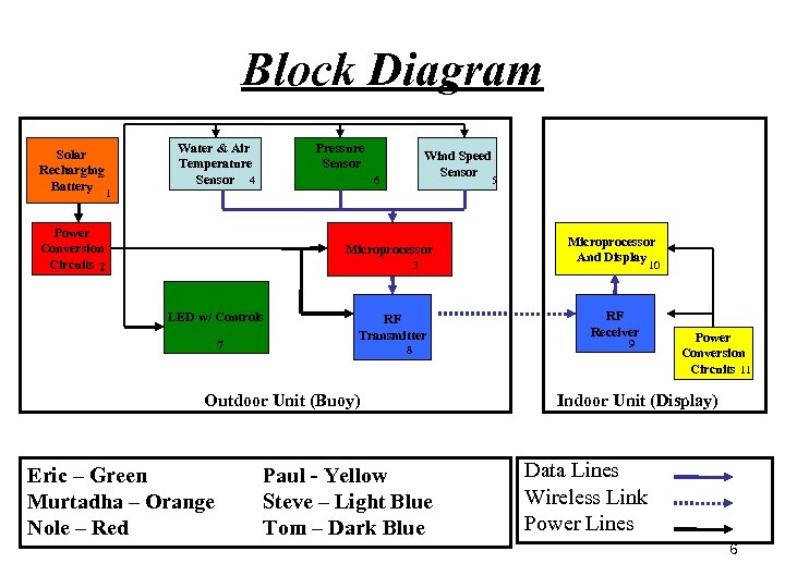 Block Diagram Solar Recharging Battery Pressure Sensor Water & Air Temperature Sensor 4 Wind Speed Sensor 6 5 1 Power Conversion Circuits 2 Microprocessor 3 LED w/ Controls 7 RF Transmitter 8 Outdoor Unit (Buoy) Eric – Green Murtadha – Orange Nole – Red Paul - Yellow Steve – Light Blue Tom – Dark Blue Microprocessor And Display 10 RF Receiver 9 Power Conversion Circuits 11 Indoor Unit (Display) Data Lines Wireless Link Power Lines 6
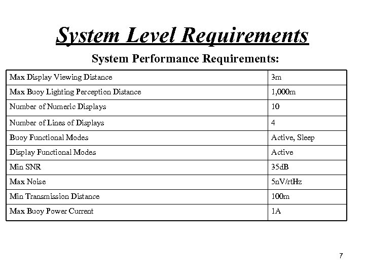 System Level Requirements System Performance Requirements: Max Display Viewing Distance 3 m Max Buoy Lighting Perception Distance 1, 000 m Number of Numeric Displays 10 Number of Lines of Displays 4 Buoy Functional Modes Active, Sleep Display Functional Modes Active Min SNR 35 d. B Max Noise 5 n. V/rt. Hz Min Transmission Distance 100 m Max Buoy Power Current 1 A 7
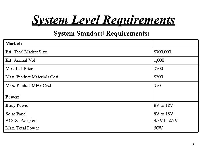 System Level Requirements System Standard Requirements: Market: Est. Total Market Size $700, 000 Est. Annual Vol. 1, 000 Min. List Price $700 Max. Product Materials Cost $300 Max. Product MFG Cost $50 Power: Buoy Power 8 V to 18 V Solar Panel AC/DC Adapter 8 V to 18 V 3. 3 V to 8. 7 V Max. Total Power 50 W 8
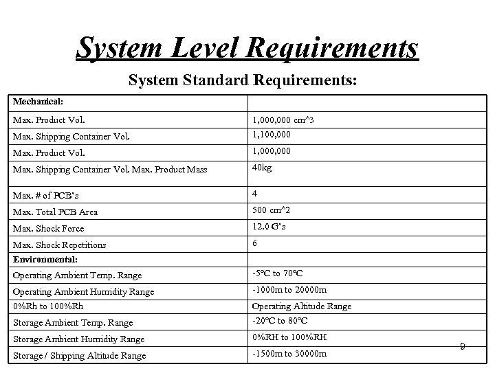 System Level Requirements System Standard Requirements: Mechanical: Max. Product Vol. 1, 000 cm^3 Max. Shipping Container Vol. 1, 100, 000 Max. Product Vol. 1, 000 Max. Shipping Container Vol. Max. Product Mass 40 kg Max. # of PCB’s 4 Max. Total PCB Area 500 cm^2 Max. Shock Force 12. 0 G’s Max. Shock Repetitions 6 Environmental: Operating Ambient Temp. Range 5°C to 70°C Operating Ambient Humidity Range 1000 m to 20000 m 0%Rh to 100%Rh Storage Ambient Temp. Range Operating Altitude Range 20°C to 80°C Storage Ambient Humidity Range 0%RH to 100%RH Storage / Shipping Altitude Range 1500 m to 30000 m 9
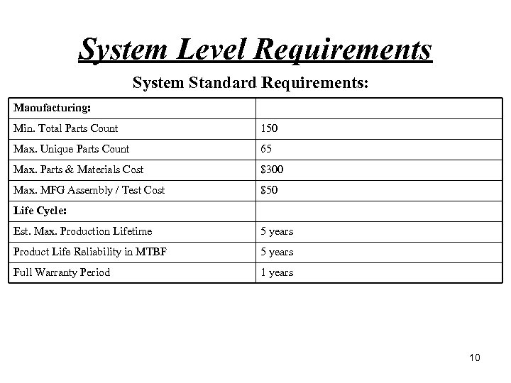 System Level Requirements System Standard Requirements: Manufacturing: Min. Total Parts Count 150 Max. Unique Parts Count 65 Max. Parts & Materials Cost $300 Max. MFG Assembly / Test Cost $50 Life Cycle: Est. Max. Production Lifetime 5 years Product Life Reliability in MTBF 5 years Full Warranty Period 1 years 10
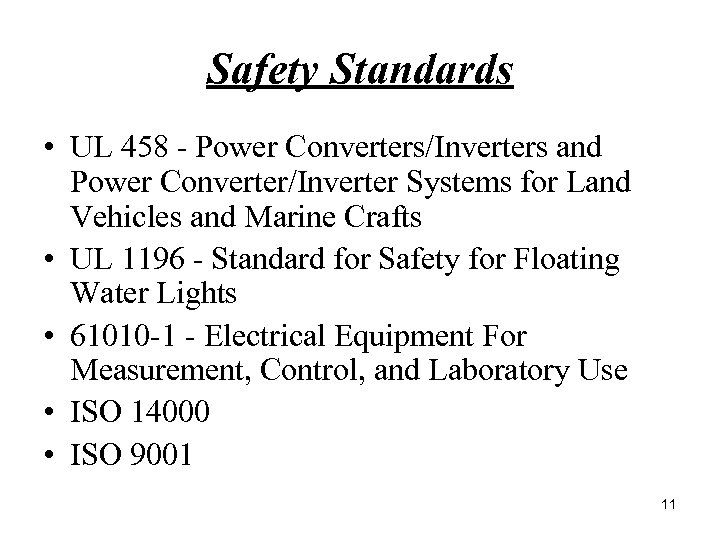 Safety Standards • UL 458 Power Converters/Inverters and Power Converter/Inverter Systems for Land Vehicles and Marine Crafts • UL 1196 Standard for Safety for Floating Water Lights • 61010 1 Electrical Equipment For Measurement, Control, and Laboratory Use • ISO 14000 • ISO 9001 11
 Basic Business Case • • Estimated Average Product Selling Price: $700 Estimated Product Annual Sales Volume: 1000 Units Estimated Per Unit Cost of Parts and Materials: $300 Estimated Per Unit Cost of Assembly, Testing and Mfg: $50 • Estimated Total Development Cost (Labor + Material): $494, 000 • Calculated Annual Sales (ASP$ x Annual Volume): $700, 000 12
 Basic Business Case • Calculated Per Unit Cost Margin (ASP$ [Parts + Materials + Mfg] x Costs$): $350 • Calculated Cost Margin (Per Unit CM$ / ASP$): 50% • Calculated Annual Cost Margin (CM% x Annual Sales$): $350, 000 • Calculated Return On Investment (Est. Dev. Cost$ / Annual CM$): 1. 411 Years. 13
 Block #1: Power Block 14
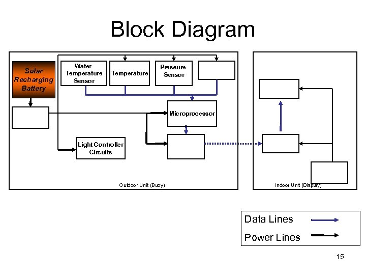 Block Diagram Solar Recharging Battery Water Temperature Sensor Air Temperature Sensor Pressure Sensor Power Conversion Circuits Wind Speed Sensor Display Unit Module Microprocessor Light Controller Circuits Outdoor Unit (Buoy) RF Transmitter RF Receiver Power Conversion Circuits Indoor Unit (Display) Data Lines Power Lines 15
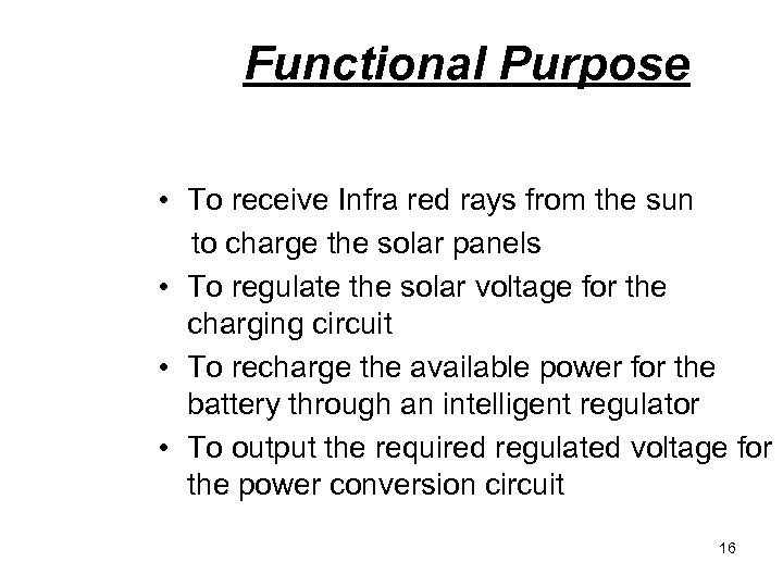 Functional Purpose • To receive Infra red rays from the sun to charge the solar panels • To regulate the solar voltage for the charging circuit • To recharge the available power for the battery through an intelligent regulator • To output the required regulated voltage for the power conversion circuit 16
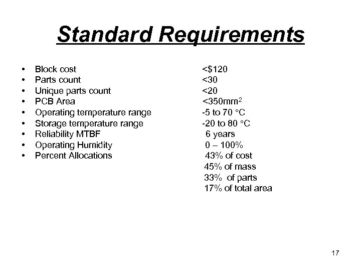 Standard Requirements • Block cost <$120 • Parts count <30 • Unique parts count <20 • PCB Area <350 mm 2 • Operating temperature range -5 to 70 C • Storage temperature range -20 to 80 C • Reliability MTBF 6 years • Operating Humidity 0 – 100% • Percent Allocations 43% of cost 45% of mass 33% of parts 17% of total area 17
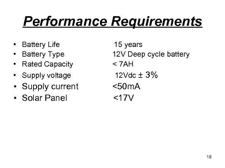 Performance Requirements • • Battery Life 15 years Battery Type 12 V Deep cycle battery Rated Capacity < 7 AH Supply voltage 12 Vdc ± 3% • Supply current <50 m. A • Solar Panel <17 V 18
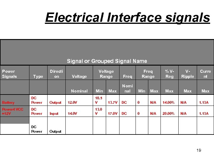 Electrical Interface signals Signal or Grouped Signal Name Power Signals Type Directi on Voltage Range Voltage Freq Range Freq % VReg VRipple Curre nt Max Min Max Nomi nal 12. 0 V 10. 5 V 13. 7 V DC 0 N/A 14. 00% N/A 1. 13 A Input 14. 0 V 13. 0 V 17. 0 V DC 0 N/A 20. 00% N/A 1. 13 A DC Power Output Battery DC Power 4 VCC +12 V DC Power Output Nominal Min Max 19
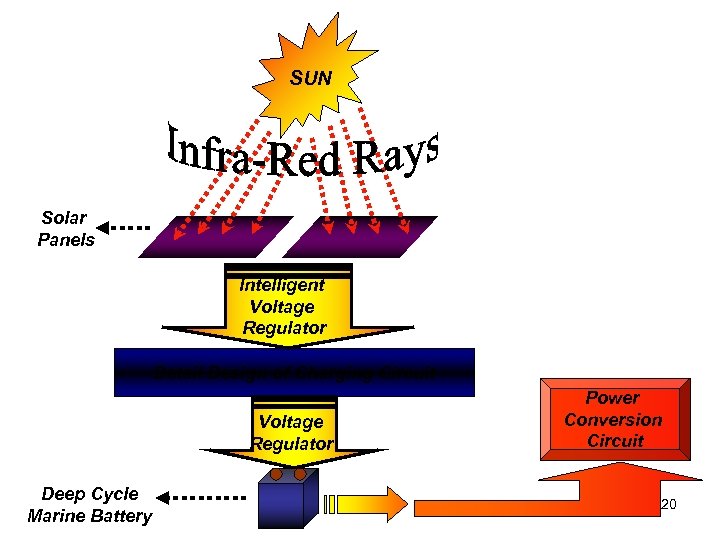 Block Interface SUN Solar Panels Intelligent Voltage Regulator Detail Design of Charging Circuit Voltage Regulator Deep Cycle Marine Battery Power Conversion Circuit 20
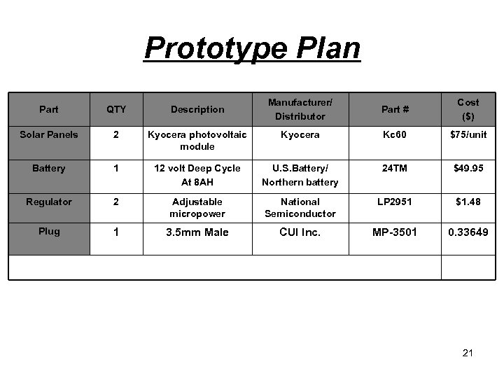 Prototype Plan Manufacturer/ Distributor Part # Cost ($) Kyocera photovoltaic module Kyocera Kc 60 $75/unit 1 12 volt Deep Cycle At 8 AH U. S. Battery/ Northern battery 24 TM $49. 95 Regulator 2 Adjustable micropower National Semiconductor LP 2951 $1. 48 Plug 1 3. 5 mm Male CUI Inc. MP-3501 0. 33649 Part QTY Description Solar Panels 2 Battery 21
 Power Regulation and Switching Nole Martin 22
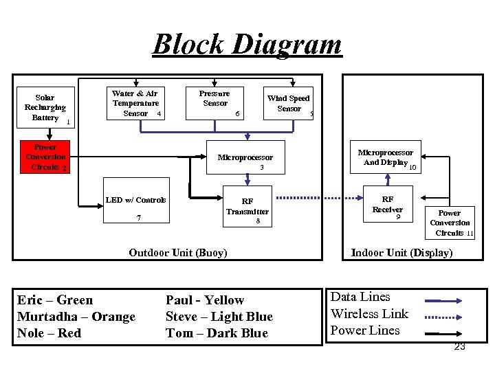 Block Diagram Solar Recharging Battery Pressure Sensor Water & Air Temperature Sensor 4 Wind Speed Sensor 6 5 1 Power Conversion Circuits 2 Microprocessor 3 LED w/ Controls 7 RF Transmitter 8 Outdoor Unit (Buoy) Eric – Green Murtadha – Orange Nole – Red Paul - Yellow Steve – Light Blue Tom – Dark Blue Microprocessor And Display 10 RF Receiver 9 Power Conversion Circuits 11 Indoor Unit (Display) Data Lines Wireless Link Power Lines 23
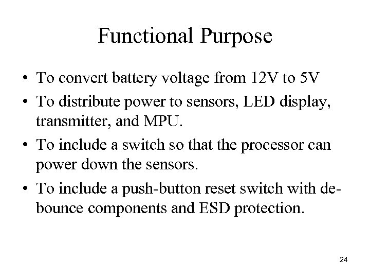 Functional Purpose • To convert battery voltage from 12 V to 5 V • To distribute power to sensors, LED display, transmitter, and MPU. • To include a switch so that the processor can power down the sensors. • To include a push button reset switch with de bounce components and ESD protection. 24
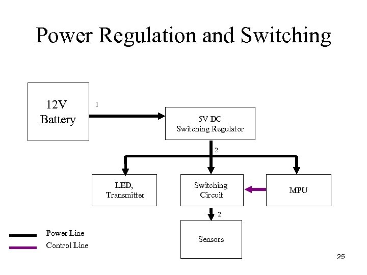 Power Regulation and Switching 12 V Battery 1 5 V DC Switching Regulator 2 LED, Transmitter Switching Circuit MPU 2 Power Line Control Line Sensors 25
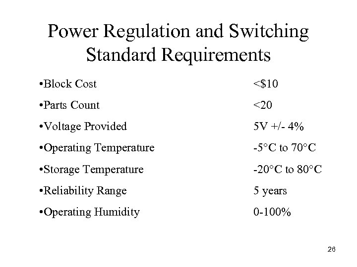 Power Regulation and Switching Standard Requirements • Block Cost <$10 • Parts Count <20 • Voltage Provided 5 V +/ 4% • Operating Temperature 5°C to 70°C • Storage Temperature 20°C to 80°C • Reliability Range 5 years • Operating Humidity 0 100% 26
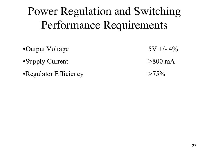 Power Regulation and Switching Performance Requirements • Output Voltage 5 V +/ 4% • Supply Current >800 m. A • Regulator Efficiency >75% 27
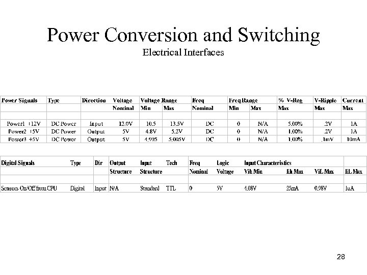 Power Conversion and Switching Electrical Interfaces 28
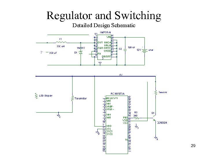 Regulator and Switching Detailed Design Schematic 29
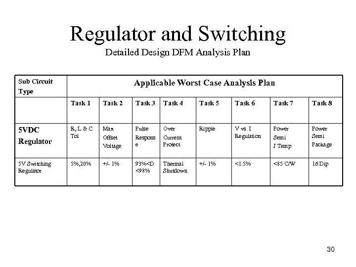 Regulator and Switching Detailed Design DFM Analysis Plan Sub Circuit Type Applicable Worst Case Analysis Plan Task 1 Task 2 Task 3 Task 4 Task 5 Task 6 Task 7 Task 8 5 VDC Regulator R, L & C Tol Max Offset Voltage Pulse Respons e Over Current Protect Ripple V vs. I Regulation Power Semi J Temp Power Semi Package 5 V Switching Regulator 5%, 20% +/ 1% 93%
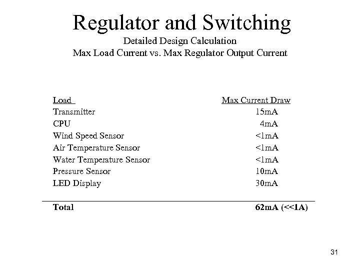 Regulator and Switching Detailed Design Calculation Max Load Current vs. Max Regulator Output Current Load Transmitter CPU Wind Speed Sensor Air Temperature Sensor Water Temperature Sensor Pressure Sensor LED Display Total Max Current Draw 15 m. A 4 m. A <1 m. A 10 m. A 30 m. A 62 m. A (<<1 A) 31
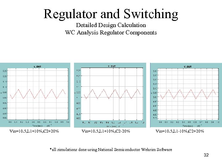 Regulator and Switching Detailed Design Calculation WC Analysis Regulator Components Vin=10. 5, L 1+10%, C 2+20% Vin=10. 5, L 1+10%, C 2 20% Vin=10. 5, L 1 10%, C 2+20% *all simulations done using National Semiconductor Websim Software 32
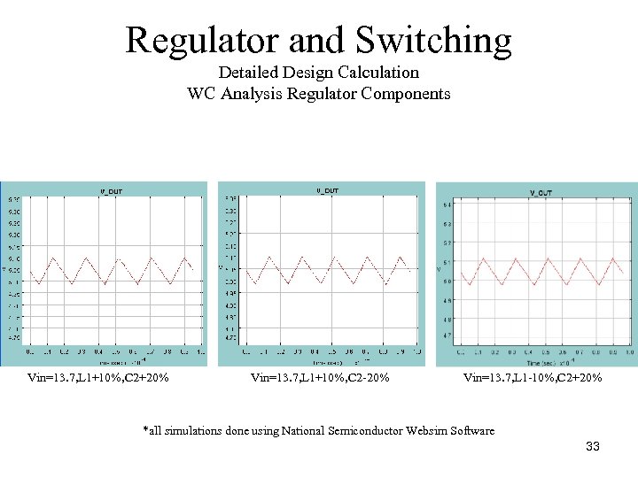 Regulator and Switching Detailed Design Calculation WC Analysis Regulator Components Vin=13. 7, L 1+10%, C 2+20% Vin=13. 7, L 1+10%, C 2 20% Vin=13. 7, L 1 10%, C 2+20% *all simulations done using National Semiconductor Websim Software 33
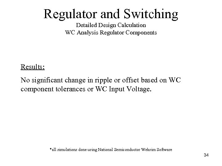 Regulator and Switching Detailed Design Calculation WC Analysis Regulator Components Results: No significant change in ripple or offset based on WC component tolerances or WC Input Voltage. *all simulations done using National Semiconductor Websim Software 34
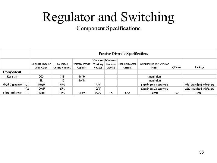 Regulator and Switching Component Specifications 35
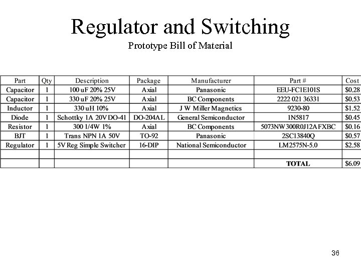 Regulator and Switching Prototype Bill of Material 36
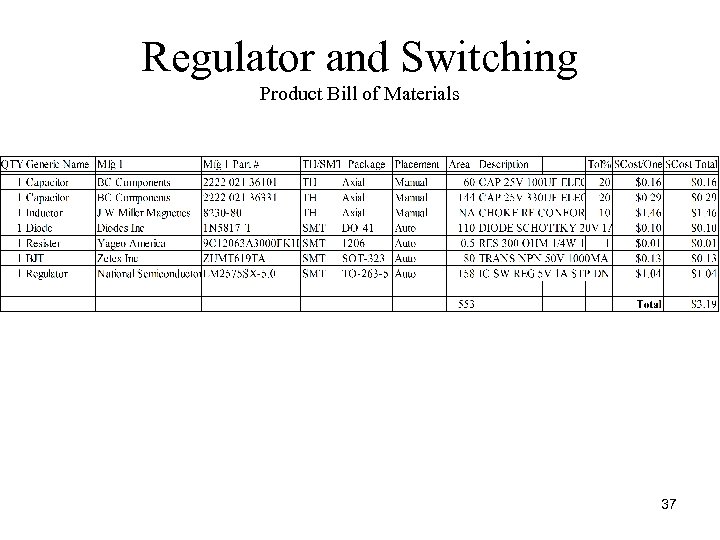 Regulator and Switching Product Bill of Materials 37
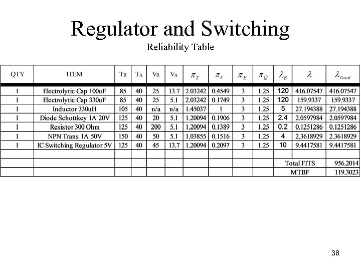 Regulator and Switching Reliability Table 38
 Regulator and Switching Summary of Reliability Table • The dominant parts for unreliability are the electrolytic capacitors. This is due to the method of approximation used as well as the voltage rating selected. • For the capacitors higher voltage rated components could be introduced to improve reliability. 39
 Regulator and Switching Obsolescence Table 40
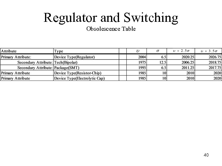
 Regulator and Switching Obsolescence Table • The worst parts for obsolescence is the SMT voltage regulator. The results do not warrant replacement. • The worst obsolescence window found was 6. 5 years. This is above the product life requirement of 5 years. 41
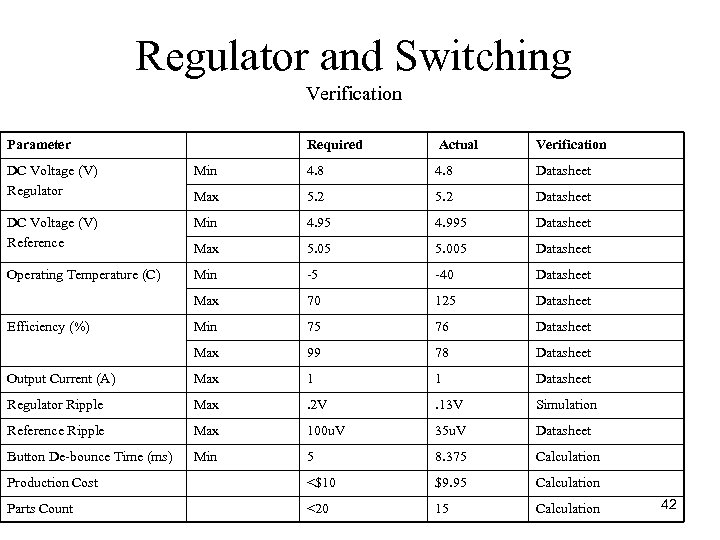 Regulator and Switching Verification Parameter Required Actual Verification DC Voltage (V) Regulator Min 4. 8 Datasheet Max 5. 2 Datasheet DC Voltage (V) Reference Min 4. 95 4. 995 Datasheet Max 5. 05 5. 005 Datasheet Operating Temperature (C) Min 5 40 Datasheet Max 70 125 Datasheet Min 75 76 Datasheet Max 99 78 Datasheet Output Current (A) Max 1 1 Datasheet Regulator Ripple Max . 2 V . 13 V Simulation Reference Ripple Max 100 u. V 35 u. V Datasheet Button De bounce Time (ms) Min 5 8. 375 Calculation Production Cost <$10 $9. 95 Calculation Parts Count <20 15 Calculation Efficiency (%) 42
 Regulator and Switching Assembly Specifications • All components for this block reside on PCB Board #1 • Testing will be performed on the regulator to ensure a clean +5 V output. 43
 Microprocessor Nole Martin 44
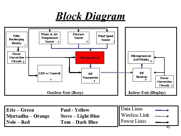 Block Diagram Solar Recharging Battery Pressure Sensor Water & Air Temperature Sensor 4 Wind Speed Sensor 6 5 1 Power Conversion Circuits 2 Microprocessor 3 LED w/ Controls 7 RF Transmitter 8 Outdoor Unit (Buoy) Eric – Green Murtadha – Orange Nole – Red Paul - Yellow Steve – Light Blue Tom – Dark Blue Microprocessor And Display 10 RF Receiver 9 Power Conversion Circuits 11 Indoor Unit (Display) Data Lines Wireless Link Power Lines 45
 Functional Purpose • Read analog outputs of the sensors and convert them to digital. • Process the results to obtain meaningful data. • Send meaningful data to the transmitter. • Control power to sensors. 46
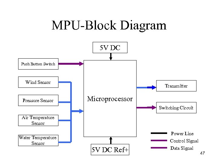 MPU Block Diagram 5 V DC Push Button Switch Wind Sensor Pressure Sensor Transmitter Microprocessor Switching Circuit Air Temperature Sensor Water Temperature Sensor 5 V DC Ref+ Power Line Control Signal Data Signal 47
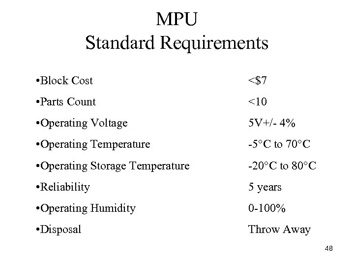 MPU Standard Requirements • Block Cost <$7 • Parts Count <10 • Operating Voltage 5 V+/ 4% • Operating Temperature 5°C to 70°C • Operating Storage Temperature 20°C to 80°C • Reliability 5 years • Operating Humidity 0 100% • Disposal Throw Away 48
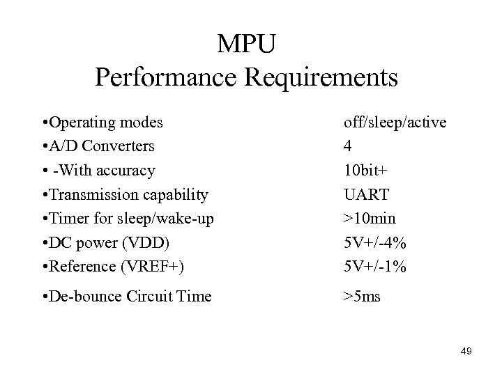 MPU Performance Requirements • Operating modes • A/D Converters • With accuracy • Transmission capability • Timer for sleep/wake up • DC power (VDD) • Reference (VREF+) • De bounce Circuit Time off/sleep/active 4 10 bit+ UART >10 min 5 V+/ 4% 5 V+/ 1% >5 ms 49
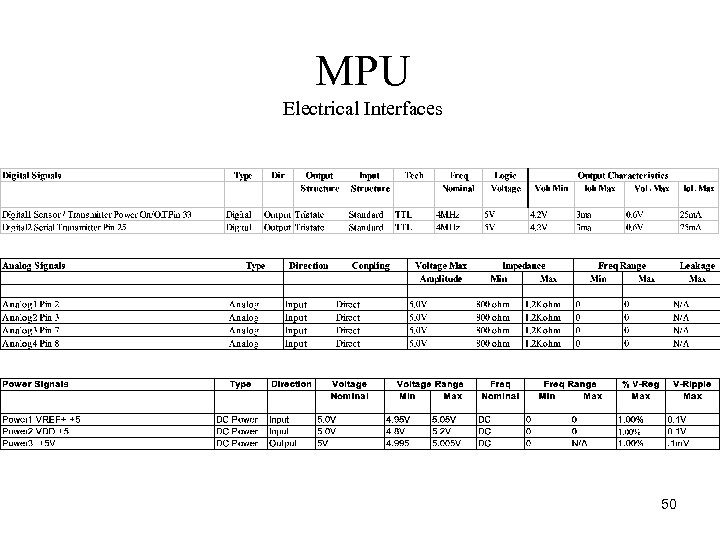 MPU Electrical Interfaces 50
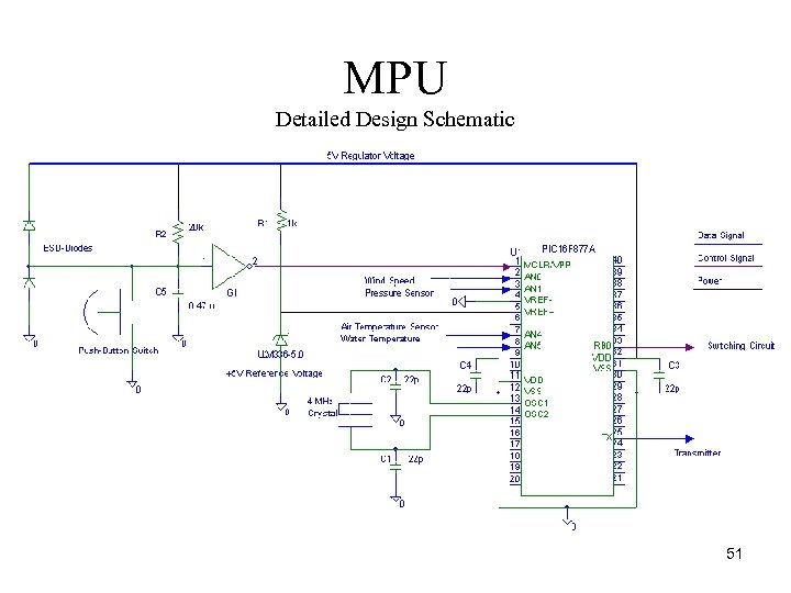 MPU Detailed Design Schematic 51
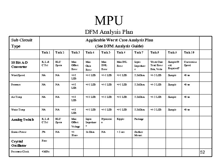 MPU DFM Analysis Plan Sub Circuit Type Applicable Worst Case Analysis Plan (See DFM Analysis Guide) Task 1 Task 2 Task 3 Task 4 Task 5 Task 6 Task 7 Task 8 Task 9 Task 10 10 Bit A-D Converter R, L & C Tol RLC Specs Max Offset Error Max Gain Error Max DNL Error Max INL Error Input Impedanc e Worst Case Total Error Bits, Volts Sample/H old Required? Conversion Speed Wind Speed NA NA +/ 2 LSB +/ 1 LSB 2. 5 k. Ohm +/ 5 LSB Sample 40 us Pressure NA NA +/ 2 LSB +/ 1 LSB 2. 5 k. Ohm +/ 5 LSB Sample 40 us Air Temp NA NA +/ 2 LSB +/ 1 LSB 2. 5 k. Ohm +/ 5 LSB Sample 40 us Water Temp NA NA +/ 2 LSB +/ 1 LSB 2. 5 k. Ohm +/ 5 LSB Sample 40 us Analog Switch R, L & C Tol RLC Specs Max Offset Input Impedanc e Hysteresi s Ripple Package 1 k Ohm NA < 5 mv Surface Mount Voltage Sensor Power 5% Crystal Oscillator Fosc Processor Clock 4 MHz NA +/ 20 mv 52
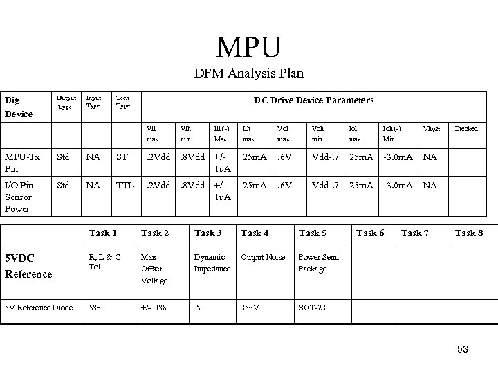 MPU DFM Analysis Plan Dig Device Output Type Input Type Tech Type DC Drive Device Parameters Vil max Vih min Iil ( ) Max Iih max Vol max Voh min Iol max Ioh ( ) Min Vhyst . 2 Vdd . 8 Vdd +/ 1 u. A 25 m. A . 6 V Vdd. 7 25 m. A 3. 0 m. A NA I/O Pin Std NA TTL. 2 Vdd. 8 Vdd Sensor Power +/ 1 u. A 25 m. A . 6 V Vdd. 7 25 m. A 3. 0 m. A NA MPU Tx Pin Std NA ST Task 1 Task 2 Task 3 Task 4 Task 5 5 VDC Reference R, L & C Tol Max Offset Voltage Dynamic Impedance Output Noise Power Semi Package 5 V Reference Diode 5% +/ . 1% . 5 35 u. V Task 6 Task 7 Checked Task 8 SOT 23 53
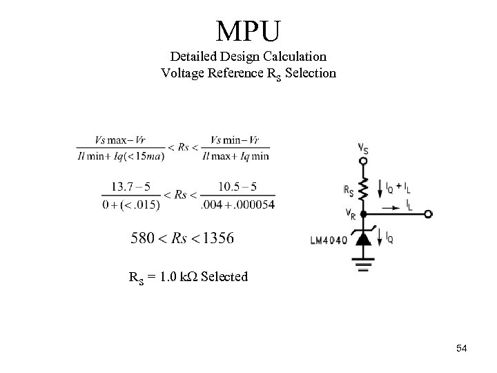 MPU Detailed Design Calculation Voltage Reference RS Selection RS = 1. 0 k Selected 54
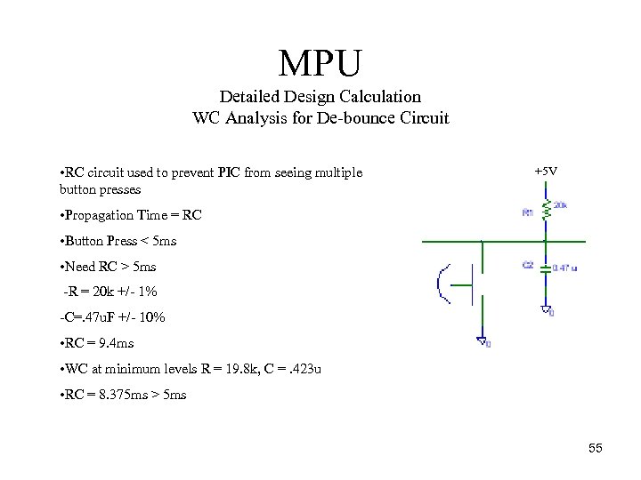 MPU Detailed Design Calculation WC Analysis for De bounce Circuit • RC circuit used to prevent PIC from seeing multiple button presses +5 V • Propagation Time = RC • Button Press < 5 ms • Need RC > 5 ms R = 20 k +/ 1% C=. 47 u. F +/ 10% • RC = 9. 4 ms • WC at minimum levels R = 19. 8 k, C =. 423 u • RC = 8. 375 ms > 5 ms 55
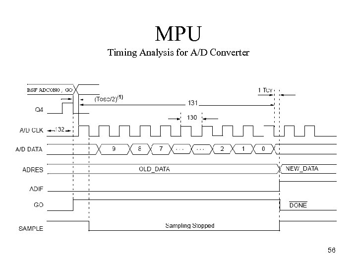 MPU Timing Analysis for A/D Converter 56
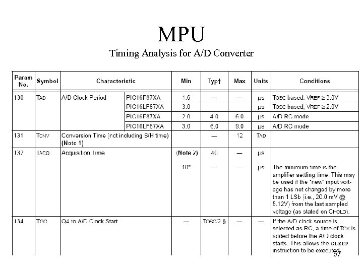 MPU Timing Analysis for A/D Converter 57
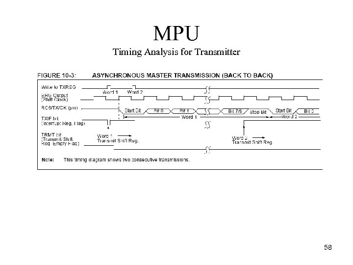 MPU Timing Analysis for Transmitter 58
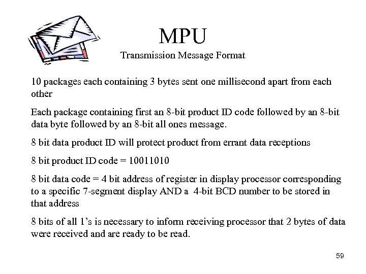 MPU Transmission Message Format 10 packages each containing 3 bytes sent one millisecond apart from each other Each package containing first an 8 bit product ID code followed by an 8 bit data byte followed by an 8 bit all ones message. 8 bit data product ID will protect product from errant data receptions 8 bit product ID code = 10011010 8 bit data code = 4 bit address of register in display processor corresponding to a specific 7 segment display AND a 4 bit BCD number to be stored in that address 8 bits of all 1’s is necessary to inform receiving processor that 2 bytes of data were received and are ready to be read. 59
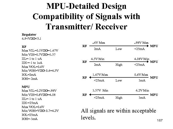
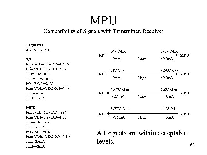 MPU Compatibility of Signals with Transmitter/ Receiver Regulator 4. 9
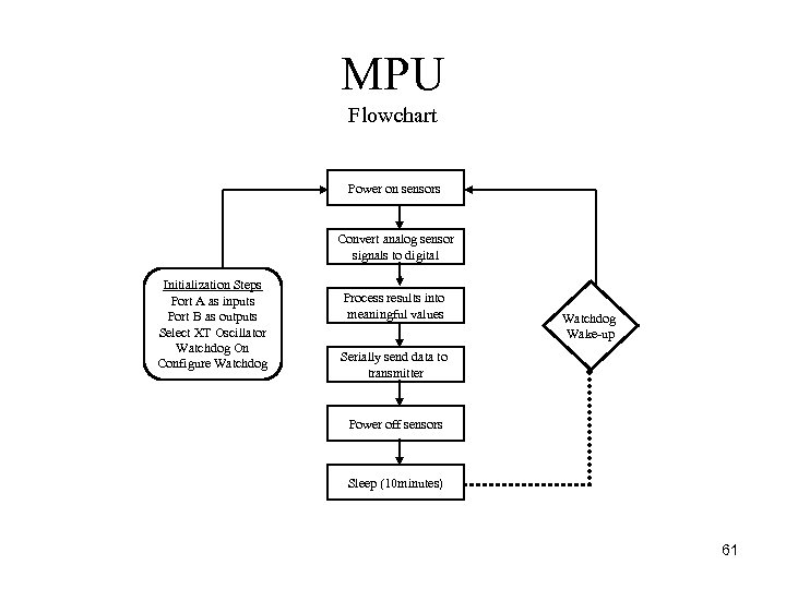 MPU Flowchart Power on sensors Convert analog sensor signals to digital Initialization Steps Port A as inputs Port B as outputs Select XT Oscillator Watchdog On Configure Watchdog Process results into meaningful values Watchdog Wake up Serially send data to transmitter Power off sensors Sleep (10 minutes) 61
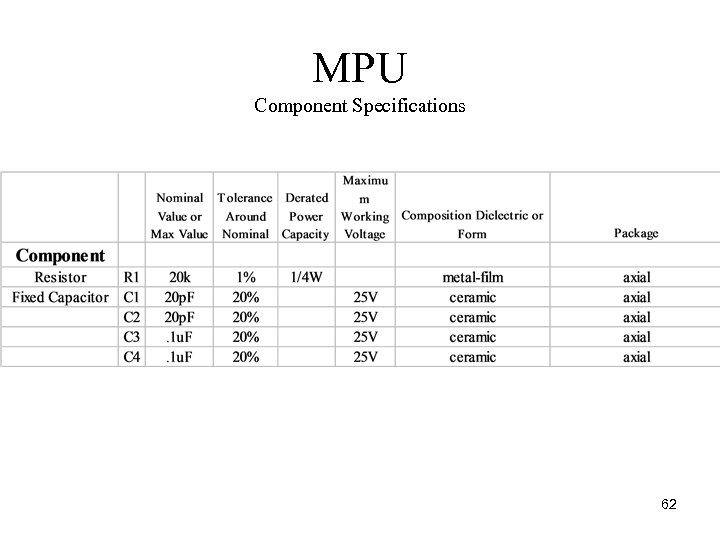 MPU Component Specifications 62
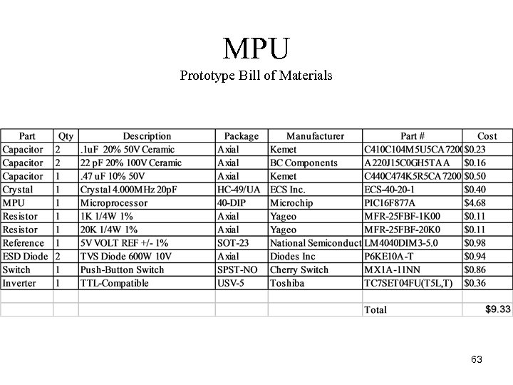 MPU Prototype Bill of Materials 63
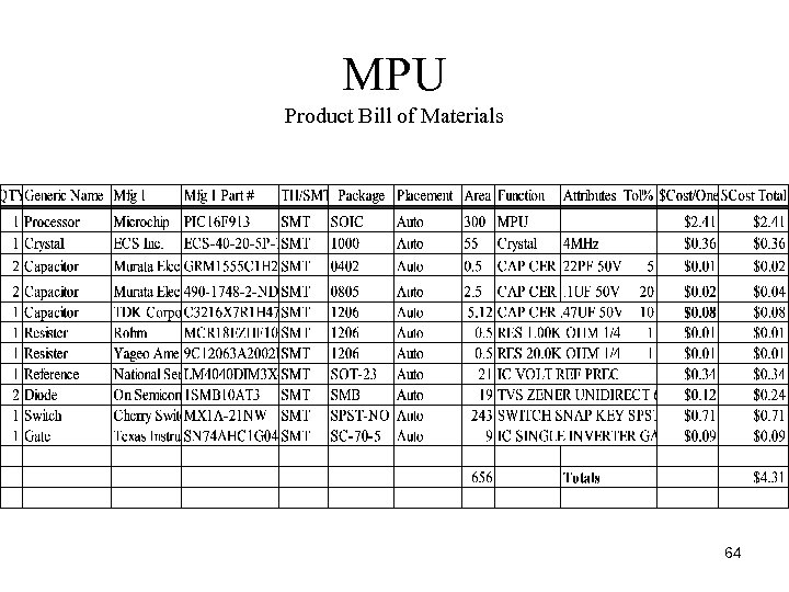 MPU Product Bill of Materials 64
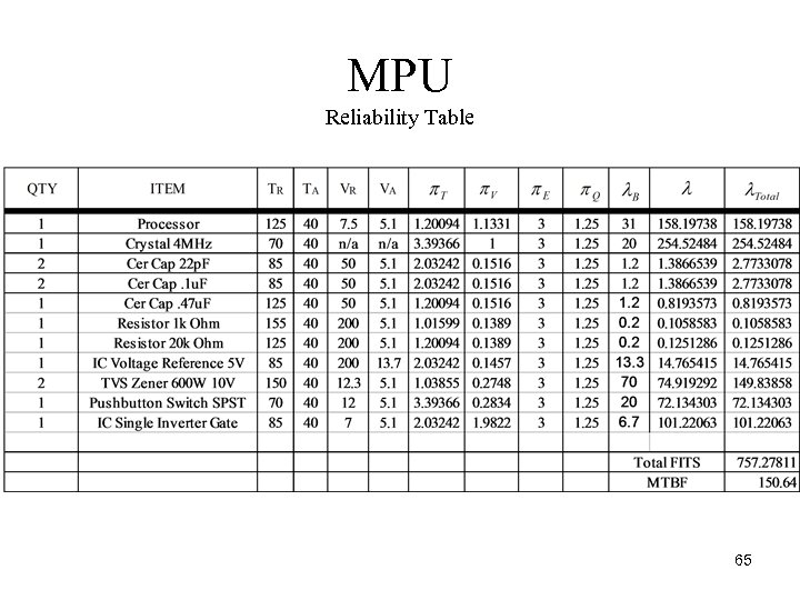 MPU Reliability Table 65
 MPU Summary of Reliability Table • The crystal, inverter gate, and ESD diodes could be considered as the worst parts for reliability. • This could be solved by finding components with higher voltage ratings. • A different method could be selected as well for better results. 66
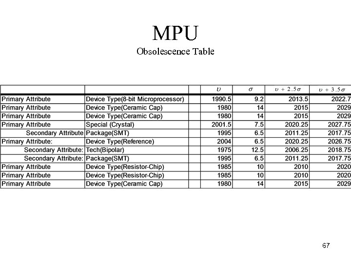 MPU Obsolescence Table 67
 MPU Summary of Obsolescence Table • The worst parts are the reference diode and the crystal. These results do not warrant replacement however. • The worst obsolescence window found was 6. 5 years. This is above the product life requirement of 5 years. 68
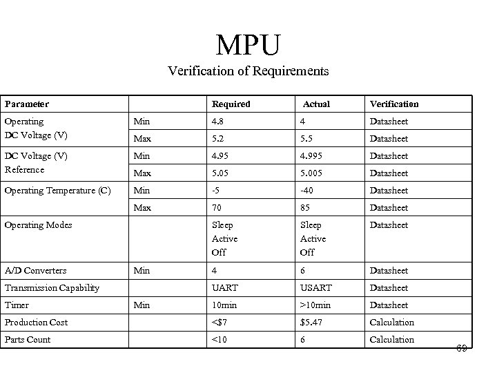 MPU Verification of Requirements Parameter Required Actual Verification Operating DC Voltage (V) Min 4. 8 4 Datasheet Max 5. 2 5. 5 Datasheet DC Voltage (V) Reference Min 4. 95 4. 995 Datasheet Max 5. 05 5. 005 Datasheet Operating Temperature (C) Min 5 40 Datasheet Max 70 85 Datasheet Sleep Active Off Datasheet 4 6 Datasheet UART USART Datasheet 10 min >10 min Datasheet Production Cost <$7 $5. 47 Calculation Parts Count <10 6 Calculation Operating Modes A/D Converters Min Transmission Capability Timer Min 69
 MPU Assembly and Testing • All components will reside on PCB #1. • Testing should be done to observe proper A/D conversion and UART transmission. 70
 Temperature Sensors Steven Krol 71
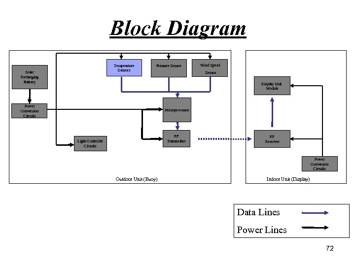 Block Diagram Temperature Sensors Solar Recharging Battery Pressure Sensor Wind Speed Sensor Display Unit Module Power Conversion Circuits Microprocessor RF Transmitter Light Controller Circuits RF Receiver Power Conversion Circuits Outdoor Unit (Buoy) Indoor Unit (Display) Data Lines Power Lines 72
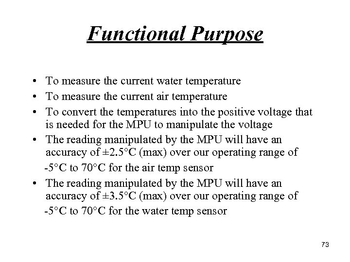 Functional Purpose • To measure the current water temperature • To measure the current air temperature • To convert the temperatures into the positive voltage that is needed for the MPU to manipulate the voltage • The reading manipulated by the MPU will have an accuracy of ± 2. 5 C (max) over our operating range of 5 C to 70 C for the air temp sensor • The reading manipulated by the MPU will have an accuracy of ± 3. 5 C (max) over our operating range of 5 C to 70 C for the water temp sensor 73
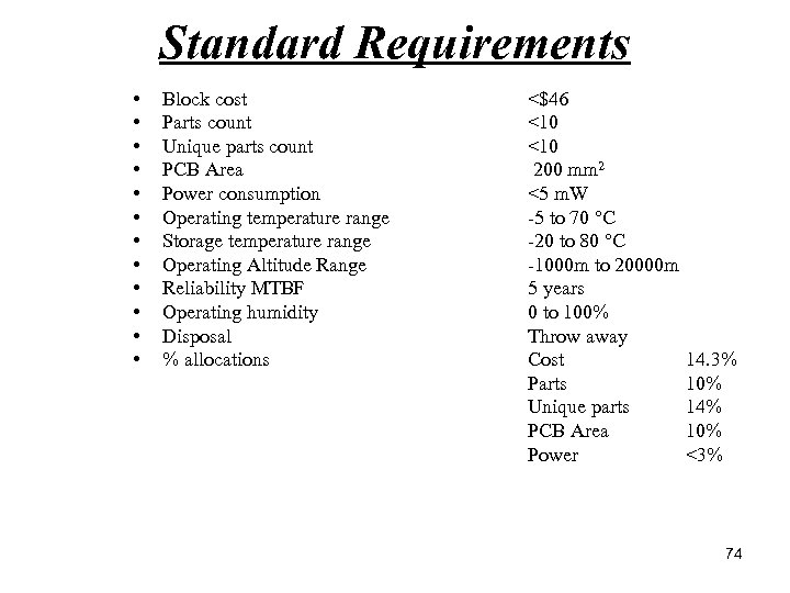 Standard Requirements • • • Block cost Parts count Unique parts count PCB Area Power consumption Operating temperature range Storage temperature range Operating Altitude Range Reliability MTBF Operating humidity Disposal % allocations <$46 <10 200 mm 2 <5 m. W 5 to 70 C 20 to 80 C 1000 m to 20000 m 5 years 0 to 100% Throw away Cost Parts Unique parts PCB Area Power 14. 3% 10% 14% 10% <3% 74
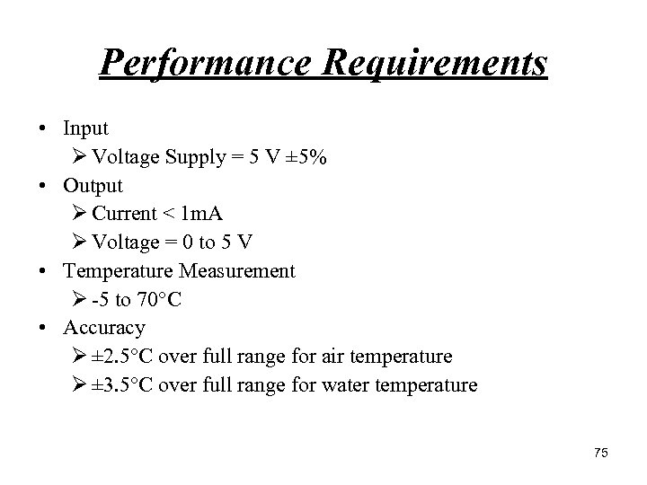 Performance Requirements • Input Ø Voltage Supply = 5 V ± 5% • Output Ø Current < 1 m. A Ø Voltage = 0 to 5 V • Temperature Measurement Ø 5 to 70 C • Accuracy Ø ± 2. 5 C over full range for air temperature Ø ± 3. 5 C over full range for water temperature 75
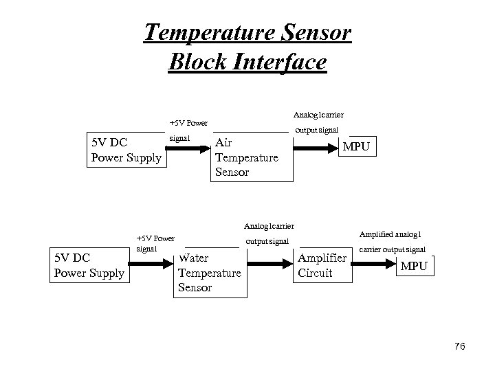 Temperature Sensor Block Interface Analog 1 carrier +5 V Power 5 V DC Power Supply signal output signal Air Temperature Sensor MPU Analog 1 carrier 5 V DC Power Supply +5 V Power signal Amplified analog 1 output signal Water Temperature Sensor Amplifier Circuit carrier output signal MPU 76
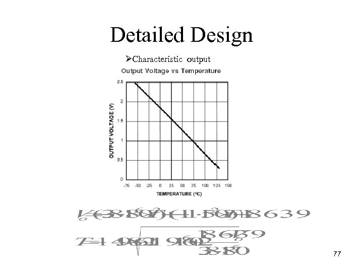 Detailed Design ØCharacteristic output 77
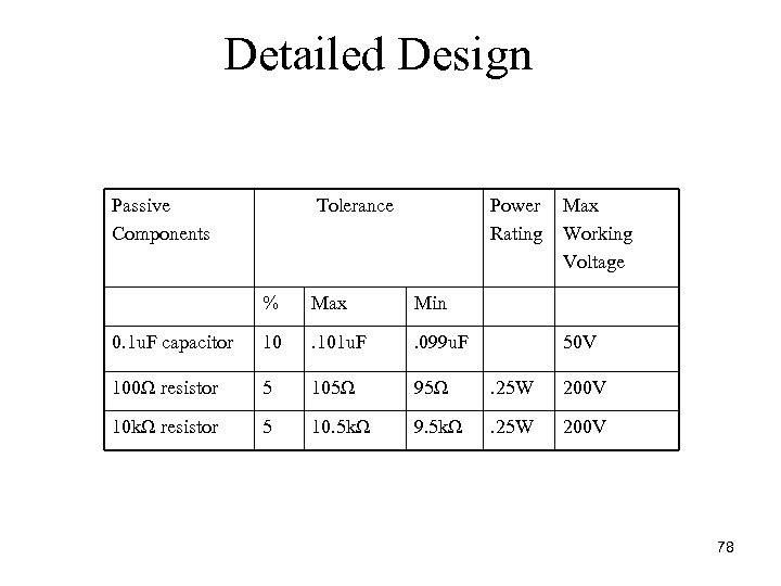 Detailed Design Passive Components Tolerance Power Rating Max Working Voltage % Max Min 0. 1 u. F capacitor 10 . 101 u. F . 099 u. F 100Ω resistor 5 105Ω 95Ω . 25 W 200 V 10 kΩ resistor 5 10. 5 kΩ 9. 5 kΩ . 25 W 200 V 50 V 78
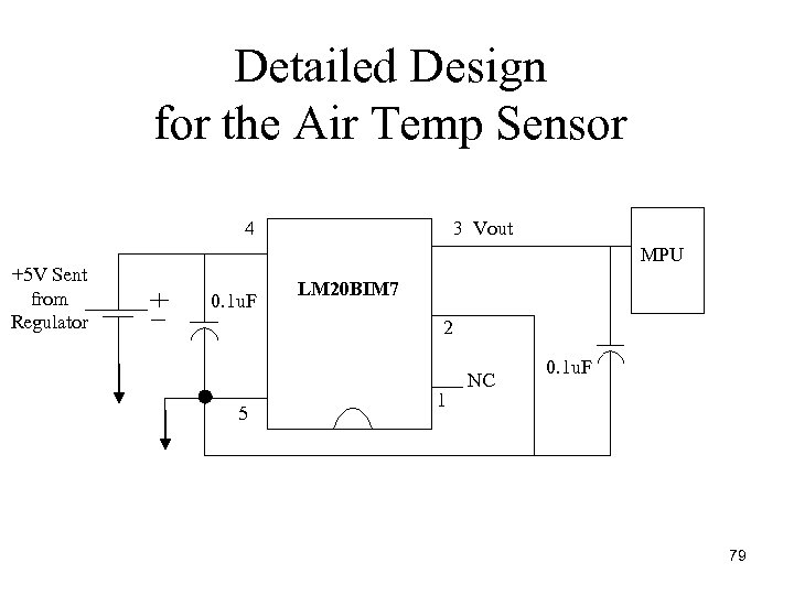 Detailed Design for the Air Temp Sensor 4 +5 V Sent from Regulator 0. 1 u. F 3 Vout LM 20 BIM 7 MPU 2 5 1 NC 0. 1 u. F 79
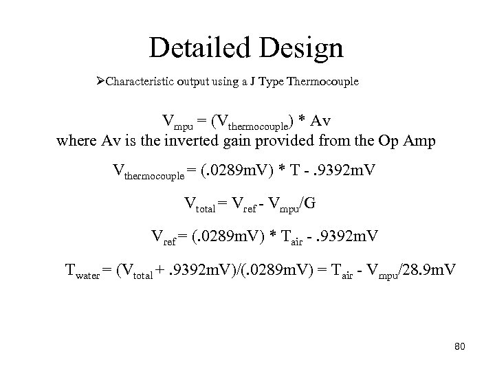 Detailed Design ØCharacteristic output using a J Type Thermocouple Vmpu = (Vthermocouple) * Av where Av is the inverted gain provided from the Op Amp Vthermocouple = (. 0289 m. V) * T . 9392 m. V Vtotal = Vref Vmpu/G Vref = (. 0289 m. V) * Tair . 9392 m. V Twater = (Vtotal +. 9392 m. V)/(. 0289 m. V) = Tair Vmpu/28. 9 m. V 80
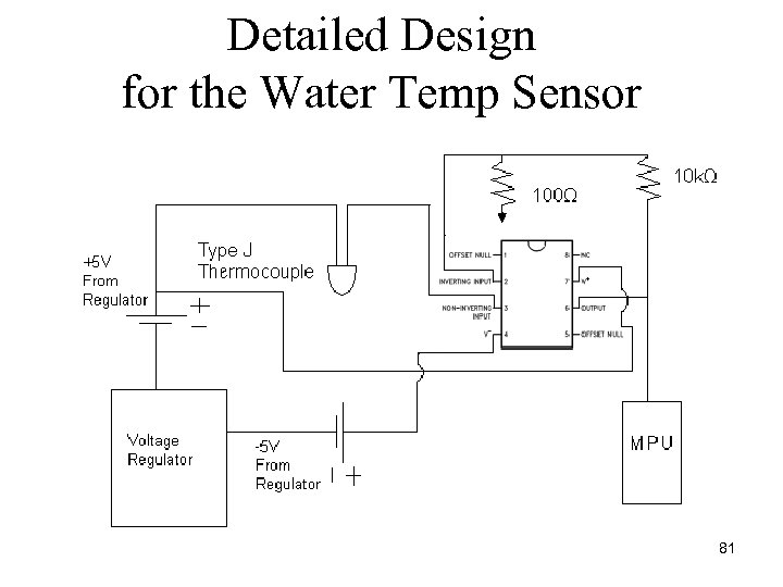 Detailed Design for the Water Temp Sensor 81
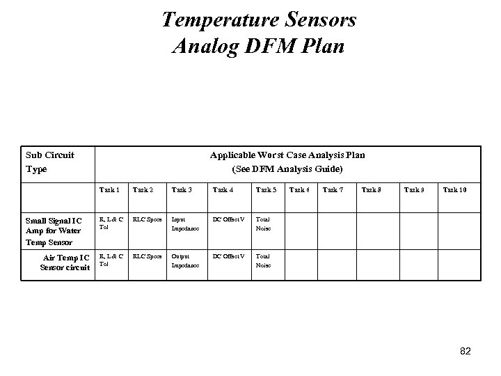 Temperature Sensors Analog DFM Plan Sub Circuit Type Applicable Worst Case Analysis Plan (See DFM Analysis Guide) Task 1 Small Signal IC Amp for Water Temp Sensor Air Temp IC Sensor circuit Task 2 Task 3 Task 4 Task 5 R, L & C Tol RLC Specs Input Impedance DC Offset V Total Noise R, L & C Tol RLC Specs Output Impedance DC Offset V Task 6 Task 7 Task 8 Task 9 Task 10 Total Noise 82
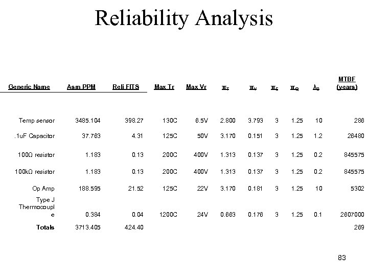 Reliability Analysis Generic Name Asm PPM Reli FITS Max Tr Max Vr πT πV πE πQ MTBF (years) λB Temp sensor 3485. 104 398. 27 130 C 6. 5 V 2. 800 3. 793 3 1. 25 10 286 . 1 u. F Capacitor 37. 763 4. 31 125 C 50 V 3. 170 0. 151 3 1. 25 1. 2 26480 100Ω resistor 1. 183 0. 13 200 C 400 V 1. 313 0. 137 3 1. 25 0. 2 845575 100 kΩ resistor 1. 183 0. 13 200 C 400 V 1. 313 0. 137 3 1. 25 0. 2 845575 Op Amp 188. 595 21. 52 125 C 22 V 3. 170 0. 181 3 1. 25 10 5302 Type J Thermocoupl e 0. 384 0. 04 1200 C 24 V 0. 663 0. 176 3 1. 25 0. 1 2607000 Totals 3713. 405 424. 40 269 83
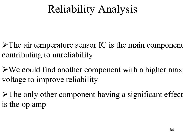 Reliability Analysis ØThe air temperature sensor IC is the main component contributing to unreliability ØWe could find another component with a higher max voltage to improve reliability ØThe only other component having a significant effect is the op amp 84
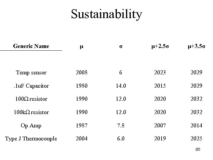 Sustainability Generic Name μ σ μ+2. 5σ μ+3. 5σ Temp sensor 2008 6 2023 2029 . 1 u. F Capacitor 1980 14. 0 2015 2029 100Ω resistor 1990 12. 0 2020 2032 100 kΩ resistor 1990 12. 0 2020 2032 Op Amp 1987 7. 8 2007 2014 Type J Thermocouple 2004 6. 0 2019 2025 85
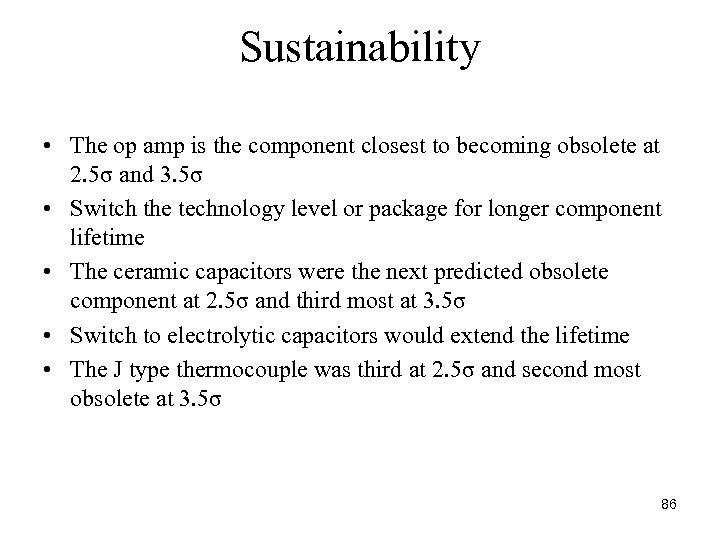 Sustainability • The op amp is the component closest to becoming obsolete at 2. 5σ and 3. 5σ • Switch the technology level or package for longer component lifetime • The ceramic capacitors were the next predicted obsolete component at 2. 5σ and third most at 3. 5σ • Switch to electrolytic capacitors would extend the lifetime • The J type thermocouple was third at 2. 5σ and second most obsolete at 3. 5σ 86
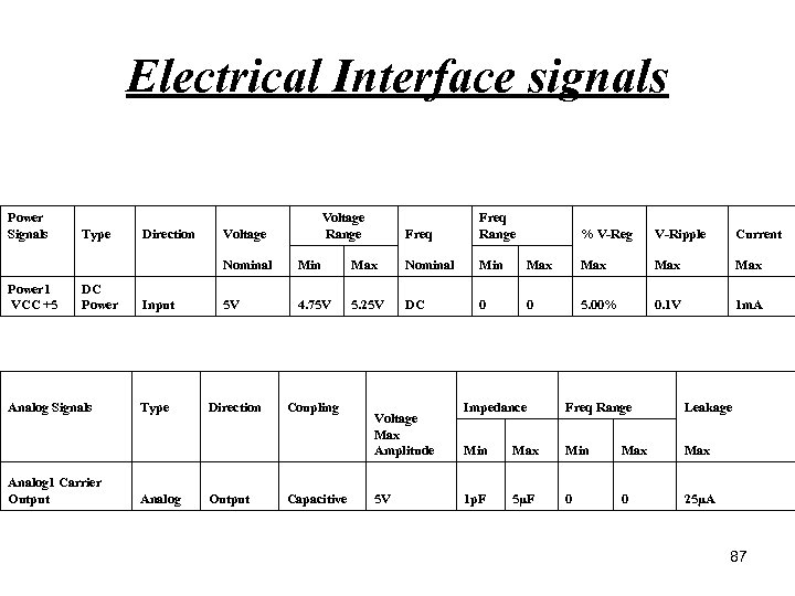 Electrical Interface signals Power Signals Type Direction Voltage Range Freq Range Nominal Min Max Nominal Min Power 1 VCC +5 DC Power Input 5 V 4. 75 V 5. 25 V DC 0 Analog Signals Type Direction Coupling Voltage Max Amplitude Analog 1 Carrier Output Analog Output Capacitive 5 V % V-Reg V-Ripple Current Max Max 0 5. 00% 0. 1 V 1 m. A Impedance Freq Range Leakage Min Max Max 1 p. F 5µF 0 0 25μA 87
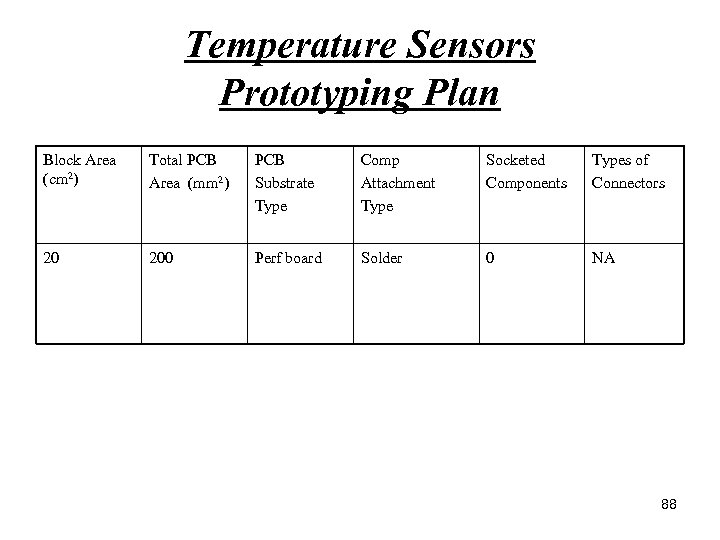 Temperature Sensors Prototyping Plan Block Area (cm 2) Total PCB Area (mm 2) PCB Substrate Type Comp Attachment Type Socketed Components Types of Connectors 20 200 Perf board Solder 0 NA 88
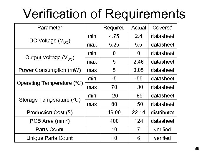 Verification of Requirements Parameter Required Actual Covered min 4. 75 2. 4 datasheet max 5. 25 5. 5 datasheet min 0 0 datasheet max 5 2. 48 datasheet max 5 0. 05 datasheet min -5 -55 datasheet max 70 130 datasheet min -20 -65 datasheet max 80 150 datasheet Production Cost ($) 46. 00 22. 14 distributor PCB Area (mm 2) 400 124 datasheet Parts Count 10 7 verified Unique Parts Count 10 6 verified DC Voltage (VDC) Output Voltage (VDC) Power Consumption (m. W) Operating Temperature ( C) Storage Temperature ( C) 89
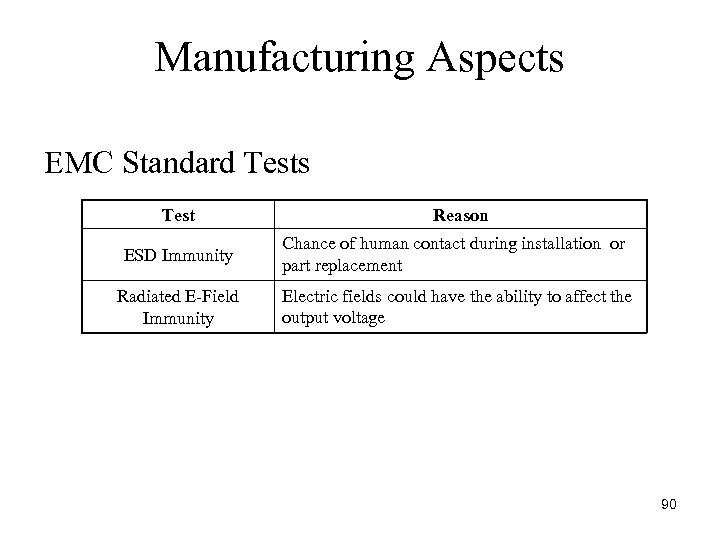 Manufacturing Aspects EMC Standard Tests Test Reason ESD Immunity Chance of human contact during installation or part replacement Radiated E Field Immunity Electric fields could have the ability to affect the output voltage 90
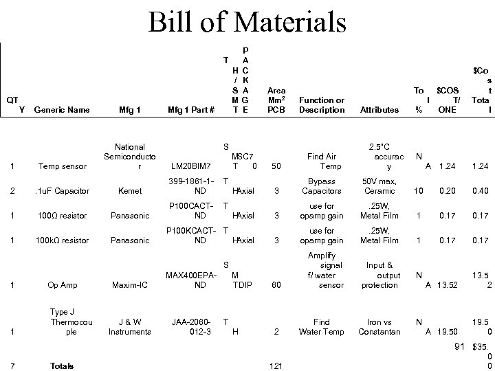 Bill of Materials H / S M T QT Y 1 2 1 1 Generic Name Mfg 1 Part # Temp sensor National Semiconducto r LM 20 BIM 7 Attributes T Panasonic P 100 CACTND Function or Description T Kemet 399 -1861 -1 ND Area Mm 2 PCB T P A C K A G E . 1 u. F Capacitor 100Ω resistor 100 kΩ resistor Panasonic S MSC 7 T 0 1 Op Amp Type J Thermocou ple JAA-2060012 -3 1. 24 3 Bypass Capacitors 50 V max, Ceramic 10 0. 20 0. 40 3 use for opamp gain . 25 W, Metal Film 1 0. 17 M TDIP 60 Amplify signal f/ water sensor Input & output protection H 2 Find Water Temp Iron vs Constantan H Axial MAX 400 EPAND J & W Instruments 50 P 100 KCACT- T ND H Axial Maxim-IC 2. 5˚C accurac y $COS l T/ % ONE Find Air Temp S 1 To $Co s t Tota l T N A 13. 52 13. 5 2 A 19. 50 19. 5 0 N 91 $35. 7 Totals 121 0 0
 Wind Sensor Steven Krol 92
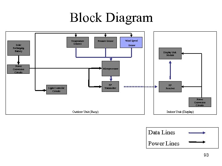 Block Diagram Temperature Sensors Solar Recharging Battery Pressure Sensor Wind Speed Sensor Display Unit Module Power Conversion Circuits Microprocessor RF Transmitter Light Controller Circuits RF Receiver Power Conversion Circuits Outdoor Unit (Buoy) Indoor Unit (Display) Data Lines Power Lines 93
 Functional Purpose • Wind is used to force an object to rotate • The wind speed sensor measures the horizontal speed of the wind converting the rate of rotation to a frequency 94
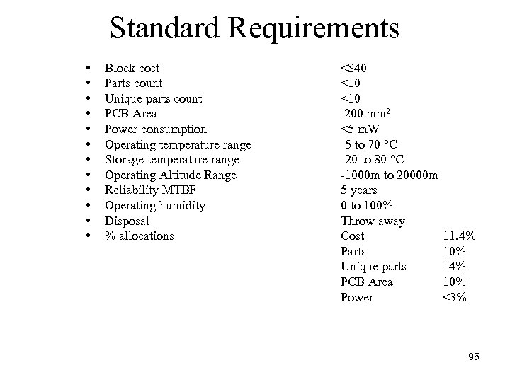 Standard Requirements • • • Block cost Parts count Unique parts count PCB Area Power consumption Operating temperature range Storage temperature range Operating Altitude Range Reliability MTBF Operating humidity Disposal % allocations <$40 <10 200 mm 2 <5 m. W 5 to 70 C 20 to 80 C 1000 m to 20000 m 5 years 0 to 100% Throw away Cost Parts Unique parts PCB Area Power 11. 4% 10% 14% 10% <3% 95
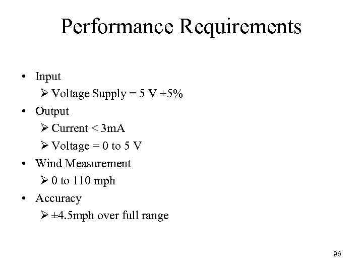 Performance Requirements • Input Ø Voltage Supply = 5 V ± 5% • Output Ø Current < 3 m. A Ø Voltage = 0 to 5 V • Wind Measurement Ø 0 to 110 mph • Accuracy Ø ± 4. 5 mph over full range 96
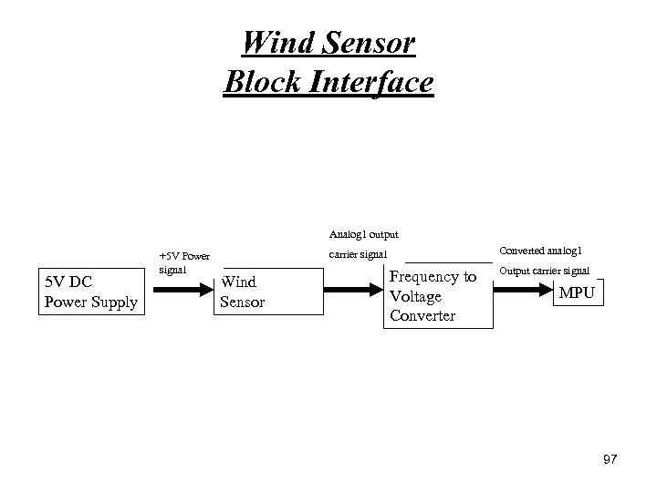 Wind Sensor Block Interface Analog 1 output 5 V DC Power Supply +5 V Power signal Converted analog 1 carrier signal Wind Sensor Frequency to Voltage Converter Output carrier signal MPU 97
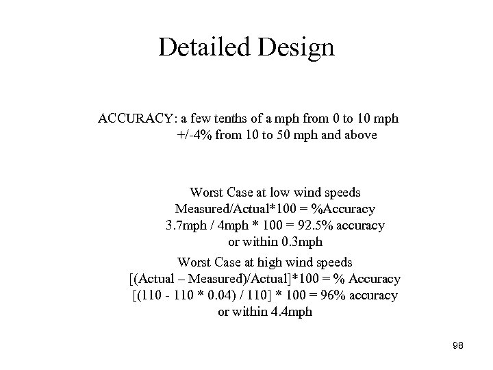 Detailed Design ACCURACY: a few tenths of a mph from 0 to 10 mph +/ 4% from 10 to 50 mph and above Worst Case at low wind speeds Measured/Actual*100 = %Accuracy 3. 7 mph / 4 mph * 100 = 92. 5% accuracy or within 0. 3 mph Worst Case at high wind speeds [(Actual – Measured)/Actual]*100 = % Accuracy [(110 * 0. 04) / 110] * 100 = 96% accuracy or within 4. 4 mph 98
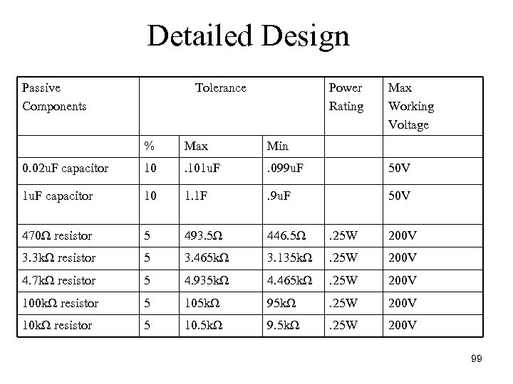 Detailed Design Passive Components Tolerance Power Rating Max Working Voltage % Max Min 0. 02 u. F capacitor 10 . 101 u. F . 099 u. F 50 V 1 u. F capacitor 10 1. 1 F . 9 u. F 50 V 470Ω resistor 5 493. 5Ω 446. 5Ω . 25 W 200 V 3. 3 kΩ resistor 5 3. 465 kΩ 3. 135 kΩ . 25 W 200 V 4. 7 kΩ resistor 5 4. 935 kΩ 4. 465 kΩ . 25 W 200 V 100 kΩ resistor 5 105 kΩ 95 kΩ . 25 W 200 V 10 kΩ resistor 5 10. 5 kΩ 9. 5 kΩ . 25 W 200 V 99
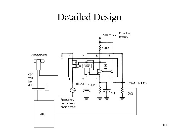 Detailed Design 100
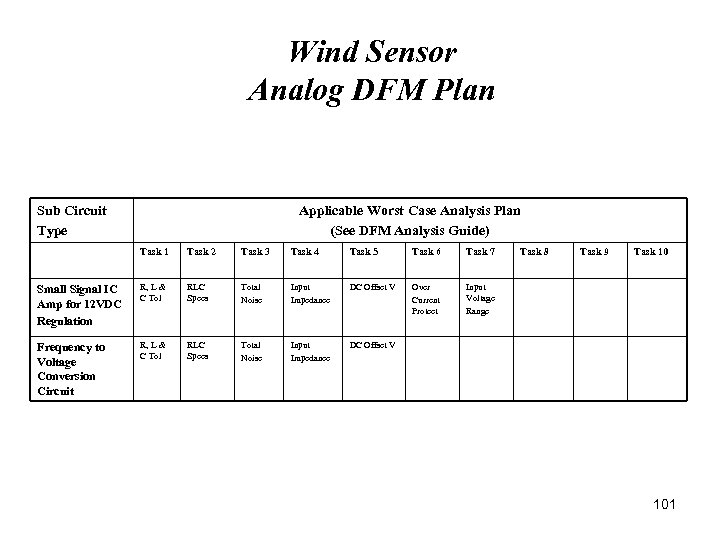 Wind Sensor Analog DFM Plan Sub Circuit Type Applicable Worst Case Analysis Plan (See DFM Analysis Guide) Task 1 Task 2 Task 3 Task 4 Task 5 Task 6 Task 7 Small Signal IC Amp for 12 VDC Regulation R, L & C Tol RLC Specs Total Noise Input Impedance DC Offset V Over Current Protect Input Voltage Range Frequency to Voltage Conversion Circuit R, L & C Tol RLC Specs Total Noise Input Impedance Task 8 Task 9 Task 10 DC Offset V 101
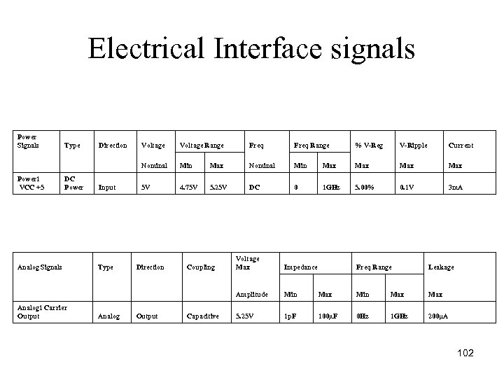 Electrical Interface signals Power Signals Type Direction Voltage Range Freq Range % V-Reg V-Ripple Current Nominal Min Max Max Max Power 1 VCC +5 DC Power Input 5 V 4. 75 V 5. 25 V DC 0 1 GHz 5. 00% 0. 1 V 3 m. A Analog Signals Type Direction Coupling Voltage Max Impedance Amplitude Min Analog 1 Carrier Output Analog Output Capacitive 5. 25 V 1 p. F Freq Range Leakage Max Min Max 100µF 0 Hz 1 GHz 200μA 102
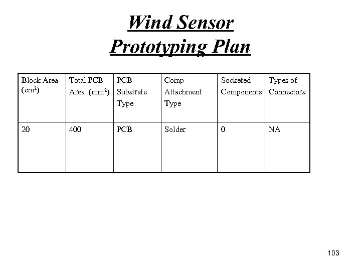 Wind Sensor Prototyping Plan Block Area (cm 2) Total PCB Area (mm 2) Substrate Type Comp Attachment Type Socketed Types of Components Connectors 20 400 Solder 0 PCB NA 103
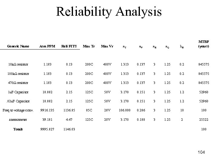 Reliability Analysis Generic Name Asm PPM Reli FITS Max Tr Max Vr πT πV πE πQ λB MTBF (years) 10 kΩ resistor 1. 183 0. 13 200 C 400 V 1. 313 0. 137 3 1. 25 0. 2 845575 100 kΩ resistor 1. 183 0. 13 200 C 400 V 1. 313 0. 137 3 1. 25 0. 2 845575 470Ω resistor 1. 183 0. 13 200 C 400 V 1. 313 0. 137 3 1. 25 0. 2 845575 1 u. F Capacitor 18. 882 2. 15 125 C 50 V 3. 170 0. 151 3 1. 25 1. 2 52960 . 02 u. F Capacitor 18. 882 2. 15 125 C 50 V 3. 170 0. 151 3 1. 25 1. 2 52960 Freq to voltage conv. 9916. 135 1136. 85 85 C 28 V 106. 000 0. 286 3 1. 25 10 100 anemometer 39. 181 4. 47 125 C 20 V 3. 170 0. 188 3 1. 25 2 25522 Totals 9995. 827 1146. 03 100 104
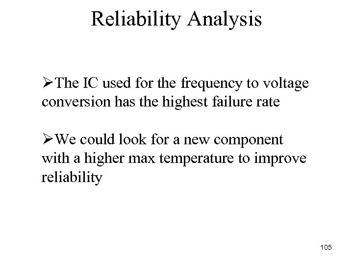 Reliability Analysis ØThe IC used for the frequency to voltage conversion has the highest failure rate ØWe could look for a new component with a higher max temperature to improve reliability 105
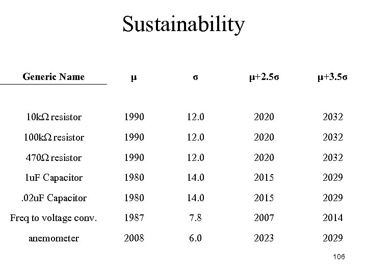 Sustainability Generic Name μ σ μ+2. 5σ μ+3. 5σ 10 kΩ resistor 1990 12. 0 2020 2032 100 kΩ resistor 1990 12. 0 2020 2032 470Ω resistor 1990 12. 0 2020 2032 1 u. F Capacitor 1980 14. 0 2015 2029 . 02 u. F Capacitor 1980 14. 0 2015 2029 Freq to voltage conv. 1987 7. 8 2007 2014 anemometer 2008 6. 0 2023 2029 106
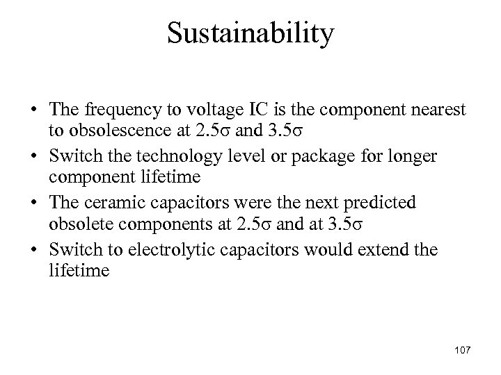 Sustainability • The frequency to voltage IC is the component nearest to obsolescence at 2. 5σ and 3. 5σ • Switch the technology level or package for longer component lifetime • The ceramic capacitors were the next predicted obsolete components at 2. 5σ and at 3. 5σ • Switch to electrolytic capacitors would extend the lifetime 107
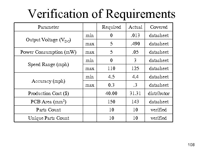 Verification of Requirements Parameter Required Actual Covered min 0 . 013 datasheet max 5 . 490 datasheet max 5 . 05 datasheet min 0 3 datasheet max 110 125 datasheet min 4. 5 4. 4 datasheet max 0. 3 datasheet Production Cost ($) 40. 00 31. 31 distributor PCB Area (mm 2) 150 143 datasheet Parts Count 10 10 verified Unique Parts Count 10 10 verified Output Voltage (VDC) Power Consumption (m. W) Speed Range (mph) Accuracy (mph) 108
 Manufacturing Aspects EMC Standard Tests Test Reason ESD Immunity Chance of human contact during installation or part replacement Radiated E Field Immunity Electric fields could have the ability to affect the output voltage 109
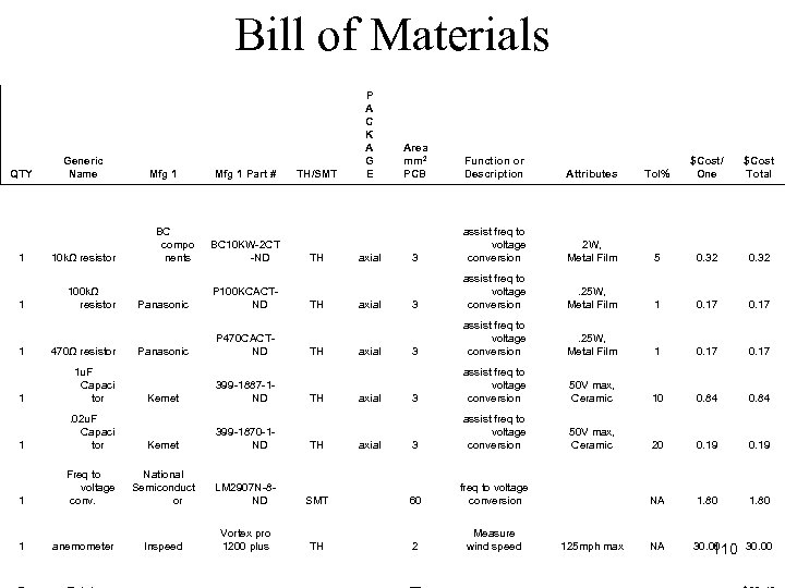 Bill of Materials QTY Generic Name Mfg 1 Part # TH/SMT P A C K A G E 1 10 kΩ resistor 1 100 kΩ resistor BC compo nents BC 10 KW-2 CT -ND TH Panasonic P 100 KCACTND Panasonic P 470 CACTND Kemet 399 -1887 -1 ND TH TH TH axial Function or Description Attributes Tol% $Cost/ One $Cost Total 3 assist freq to voltage conversion 2 W, Metal Film 5 0. 32 3 assist freq to voltage conversion . 25 W, Metal Film 1 0. 17 3 assist freq to voltage conversion 50 V max, Ceramic 10 0. 84 3 assist freq to voltage conversion 50 V max, Ceramic 20 0. 19 NA 1. 80 NA 30. 00 110 30. 00 1 470Ω resistor 1 1 u. F Capaci tor 1 . 02 u. F Capaci tor Kemet 399 -1870 -1 ND 1 Freq to voltage conv. National Semiconduct or LM 2907 N-8 ND SMT 60 freq to voltage conversion 1 anemometer Inspeed Vortex pro 1200 plus TH 2 Measure wind speed TH axial Area mm 2 PCB axial 125 mph max
 RF Transmitter Tom Reuter 111
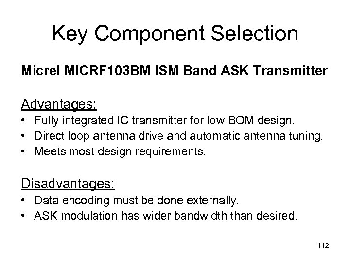 Key Component Selection Micrel MICRF 103 BM ISM Band ASK Transmitter Advantages: • Fully integrated IC transmitter for low BOM design. • Direct loop antenna drive and automatic antenna tuning. • Meets most design requirements. Disadvantages: • Data encoding must be done externally. • ASK modulation has wider bandwidth than desired. 112
 Key Component Selection Requirement Supply Voltage 4. 9 to 5. 1 VDC MICRF 103 BM Spec 4. 75 to 5. 5 VDC Supply Current 20 m. A max 18. 5 m. A max Transmission Distance Transmission Frequency Modulation Type 100 meters ~100 meters (@ 9600 bps) 862 MHz to 928 MHz Frequency Shift Keying 800 MHz to 1 GHz selected w/ crystal ASK 113
 MICRF 103 BM Schematic 114
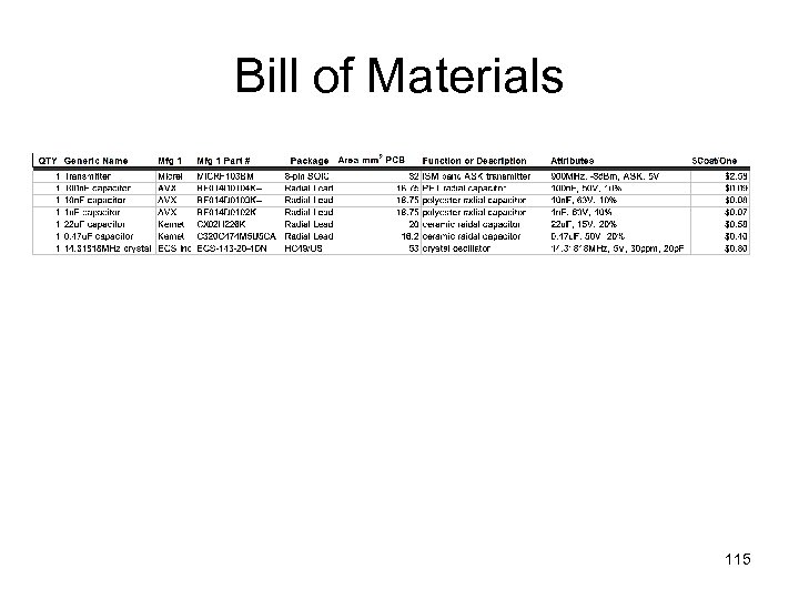 Bill of Materials 115
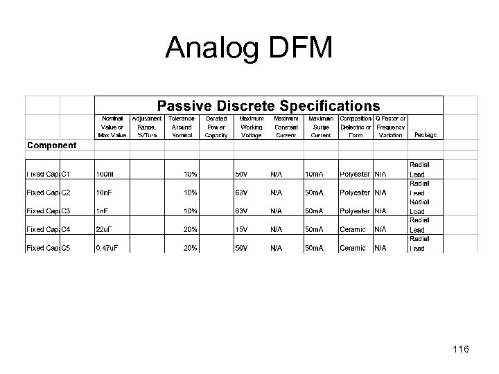 Analog DFM 116
 Analog DFM Analog Worst-Case Analyses: • • Voltage or Current Transfer Function Maximum Offset Voltage Phase vs. Frequency vs. Component Variations Output Impedance Open Loop Phase Margin Pole & Zero Locations (Fosc) Noise and/or Ripple Semiconductor Package & Heatsink 117
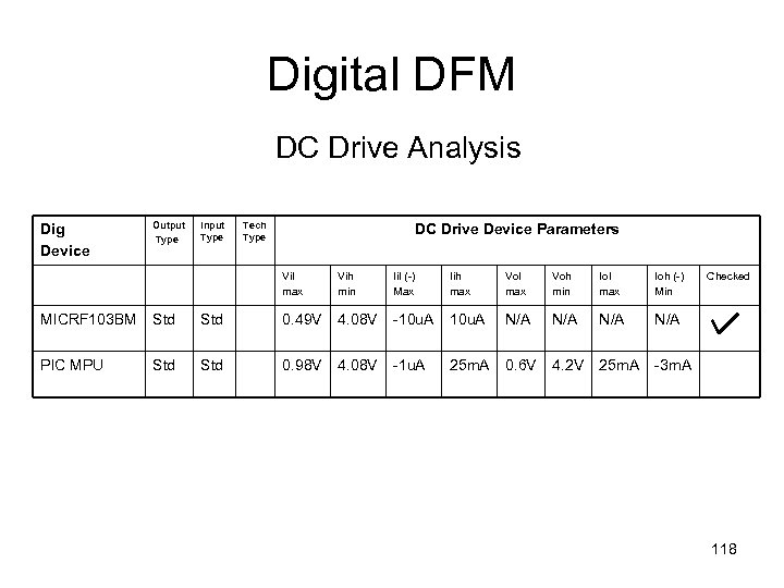 Digital DFM DC Drive Analysis Dig Device Output Type Input Type Tech Type DC Drive Device Parameters Vil max Vih min Iil (-) Max Iih max Vol max Voh min Iol max Ioh (-) Min MICRF 103 BM Std 0. 49 V 4. 08 V -10 u. A N/A N/A PIC MPU Std 0. 98 V 4. 08 V -1 u. A 25 m. A 0. 6 V 4. 2 V 25 m. A Checked -3 m. A 118
 Pressure Sensor Eric Ritzke 119
 Functional Purpose Ø The pressure sensor sends a voltage to the CPU to accurately measure pressure in kilopascals (k. Pa). Ø Allows for the prediction of weather with change in pressure. 120
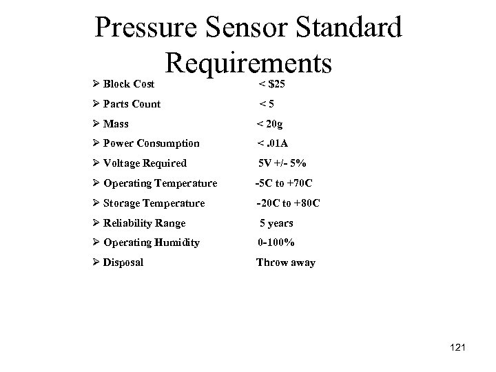 Pressure Sensor Standard Requirements Ø Block Cost < $25 Ø Parts Count < 5 Ø Mass < 20 g Ø Power Consumption <. 01 A Ø Voltage Required 5 V +/- 5% Ø Operating Temperature -5 C to +70 C Ø Storage Temperature -20 C to +80 C Ø Reliability Range 5 years Ø Operating Humidity 0 -100% Ø Disposal Throw away 121
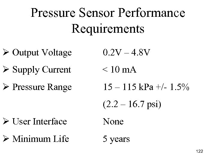 Pressure Sensor Performance Requirements Ø Output Voltage 0. 2 V – 4. 8 V Ø Supply Current < 10 m. A Ø Pressure Range 15 – 115 k. Pa +/ 1. 5% (2. 2 – 16. 7 psi) Ø User Interface None Ø Minimum Life 5 years 122
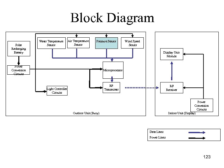 Block Diagram Solar Recharging Battery Water Temperature Sensor Air Temperature Sensor Pressure Sensor Wind Speed Sensor Display Unit Module Power Conversion Circuits Microprocessor RF Transmitter Light Controller Circuits RF Receiver Power Conversion Circuits Indoor Unit (Display) Outdoor Unit (Buoy) Data Lines Power Lines 123
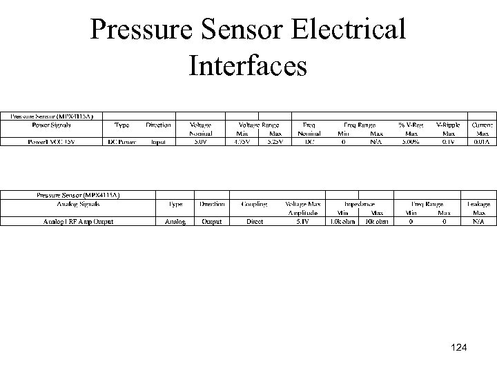 Pressure Sensor Electrical Interfaces 124
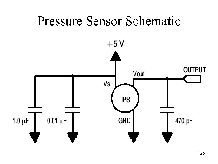 Pressure Sensor Schematic 125
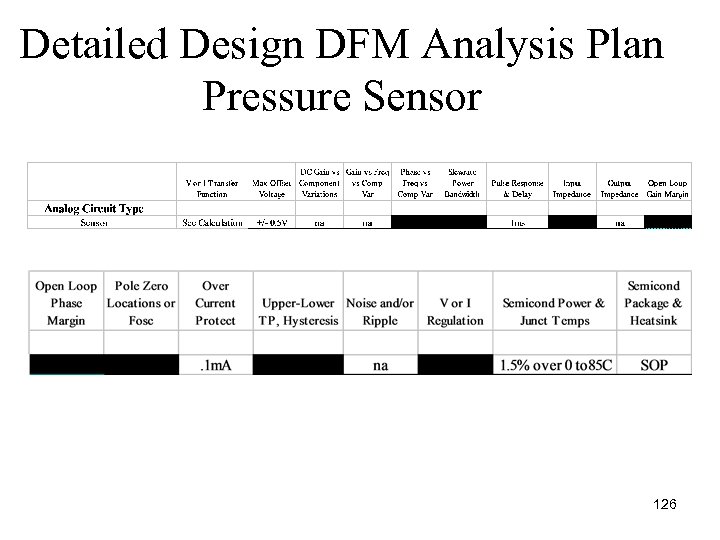 Detailed Design DFM Analysis Plan Pressure Sensor 126
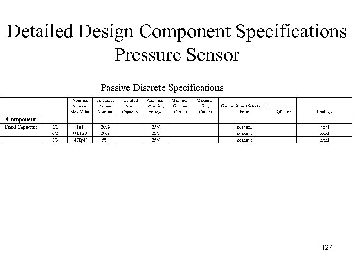 Detailed Design Component Specifications Pressure Sensor Passive Discrete Specifications 127
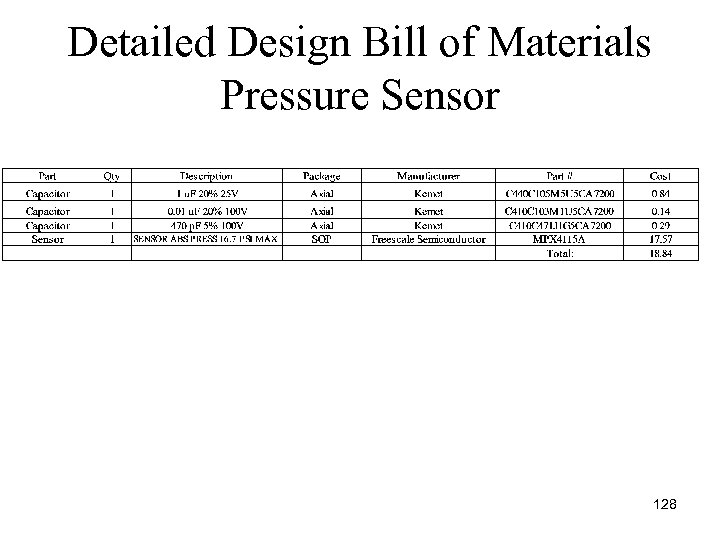 Detailed Design Bill of Materials Pressure Sensor 128
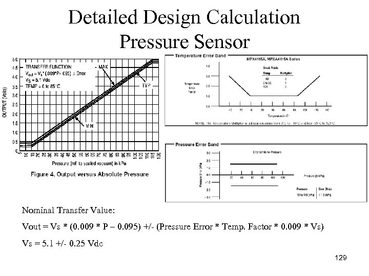 Detailed Design Calculation Pressure Sensor Nominal Transfer Value: Vout = Vs * (0. 009 * P – 0. 095) +/ (Pressure Error * Temp. Factor * 0. 009 * Vs) Vs = 5. 1 +/ 0. 25 Vdc 129
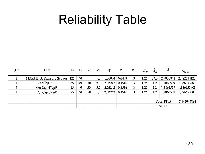 Reliability Table 130
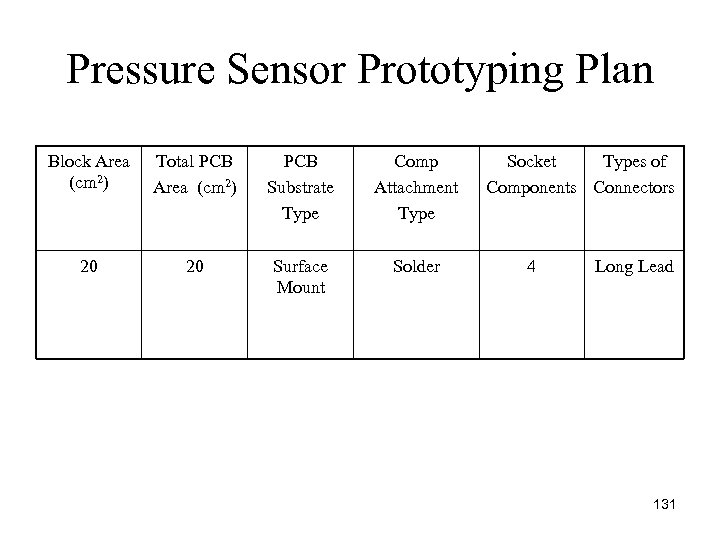 Pressure Sensor Prototyping Plan Block Area (cm 2) Total PCB Area (cm 2) PCB Substrate Type Comp Attachment Type 20 20 Surface Mount Solder Socket Types of Components Connectors 4 Long Lead 131
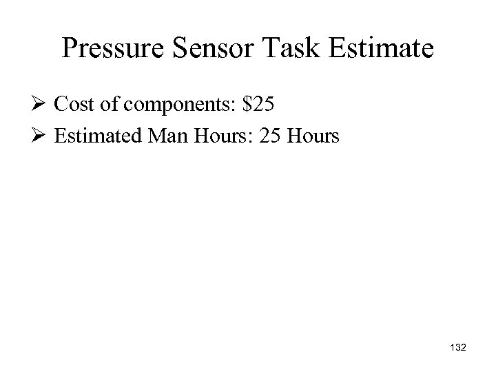 Pressure Sensor Task Estimate Ø Cost of components: $25 Ø Estimated Man Hours: 25 Hours 132
 Light Controller Circuit Eric Ritzke 133
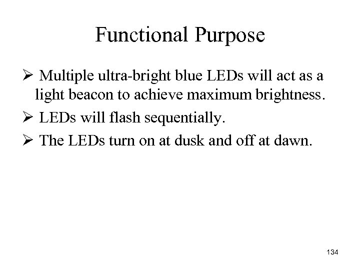 Functional Purpose Ø Multiple ultra bright blue LEDs will act as a light beacon to achieve maximum brightness. Ø LEDs will flash sequentially. Ø The LEDs turn on at dusk and off at dawn. 134
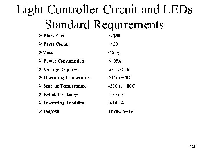 Light Controller Circuit and LEDs Standard Requirements Ø Block Cost < $30 Ø Parts Count < 30 ØMass < 50 g Ø Power Consumption <. 05 A Ø Voltage Required 5 V +/- 5% Ø Operating Temperature -5 C to +70 C Ø Storage Temperature -20 C to +80 C Ø Reliability Range 5 years Ø Operating Humidity 0 -100% Ø Disposal Throw away 135
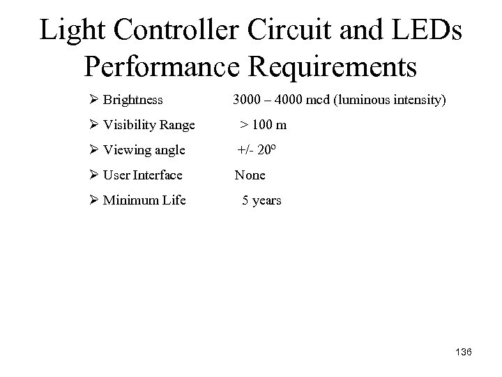 Light Controller Circuit and LEDs Performance Requirements Ø Brightness 3000 – 4000 mcd (luminous intensity) Ø Visibility Range > 100 m Ø Viewing angle +/ 20º Ø User Interface None Ø Minimum Life 5 years 136
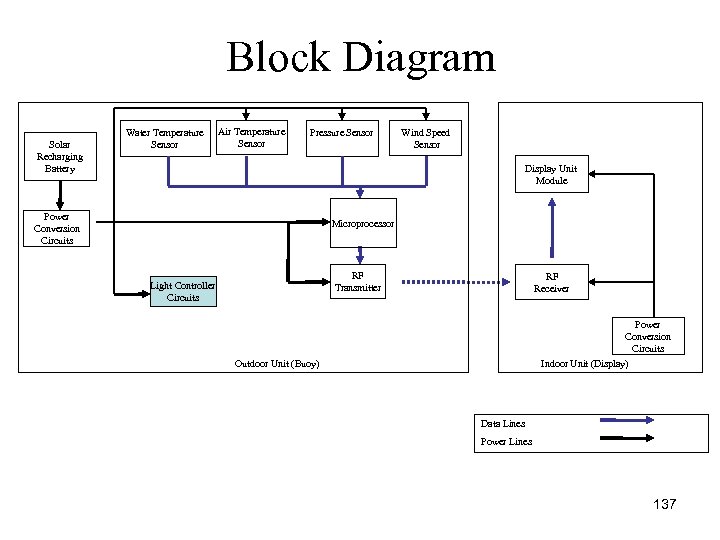 Block Diagram Solar Recharging Battery Water Temperature Sensor Air Temperature Sensor Pressure Sensor Wind Speed Sensor Display Unit Module Power Conversion Circuits Microprocessor RF Transmitter Light Controller Circuits RF Receiver Power Conversion Circuits Outdoor Unit (Buoy) Indoor Unit (Display) Data Lines Power Lines 137
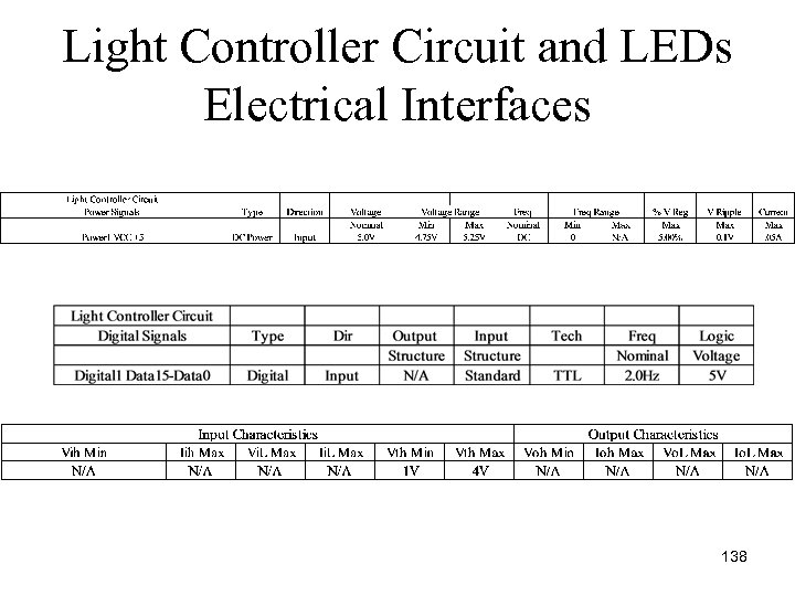 Light Controller Circuit and LEDs Electrical Interfaces 138
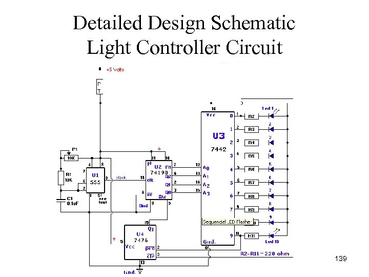 Detailed Design Schematic Light Controller Circuit 139
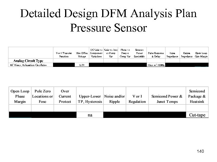 Detailed Design DFM Analysis Plan Pressure Sensor 140
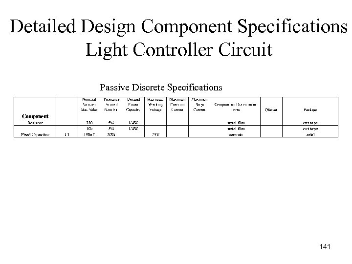 Detailed Design Component Specifications Light Controller Circuit Passive Discrete Specifications 141
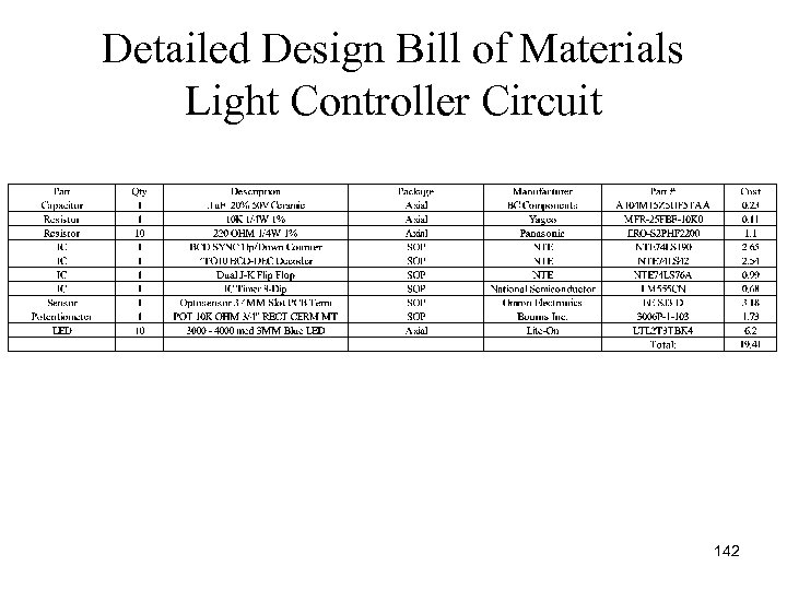 Detailed Design Bill of Materials Light Controller Circuit 142
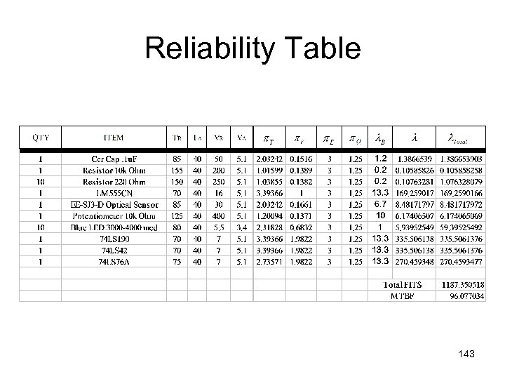 Reliability Table 143
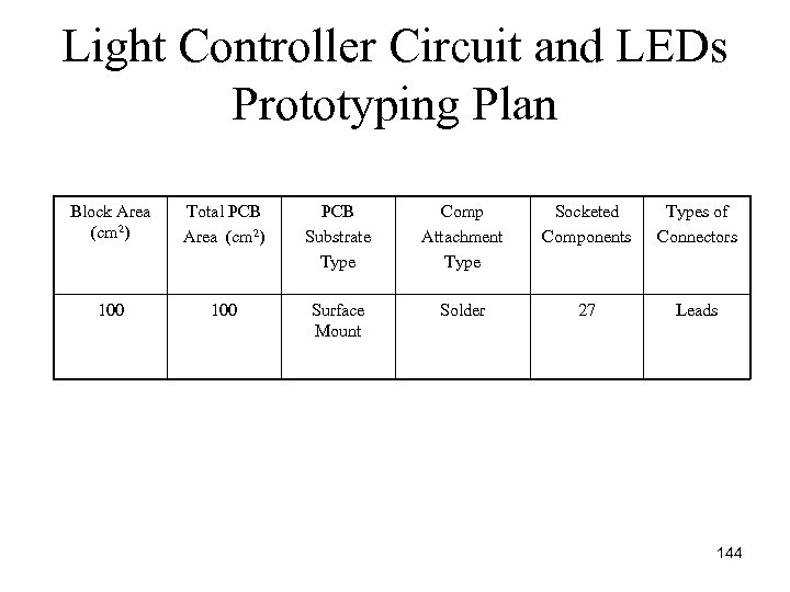 Light Controller Circuit and LEDs Prototyping Plan Block Area (cm 2) Total PCB Area (cm 2) PCB Substrate Type Comp Attachment Type Socketed Components Types of Connectors 100 Surface Mount Solder 27 Leads 144
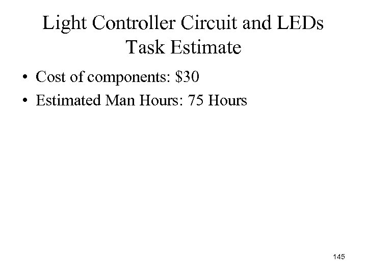 Light Controller Circuit and LEDs Task Estimate • Cost of components: $30 • Estimated Man Hours: 75 Hours 145
 RF Receiver Tom Reuter 146
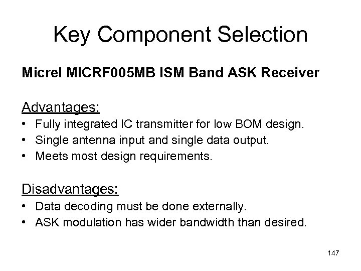 Key Component Selection Micrel MICRF 005 MB ISM Band ASK Receiver Advantages: • Fully integrated IC transmitter for low BOM design. • Single antenna input and single data output. • Meets most design requirements. Disadvantages: • Data decoding must be done externally. • ASK modulation has wider bandwidth than desired. 147
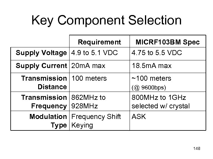 Key Component Selection Requirement Supply Voltage 4. 9 to 5. 1 VDC MICRF 103 BM Spec 4. 75 to 5. 5 VDC Supply Current 20 m. A max 18. 5 m. A max Transmission Distance Transmission Frequency Modulation Type 100 meters ~100 meters (@ 9600 bps) 862 MHz to 928 MHz Frequency Shift Keying 800 MHz to 1 GHz selected w/ crystal ASK 148
 MICRF 103 BM Schematic 149
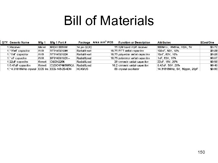 Bill of Materials 150
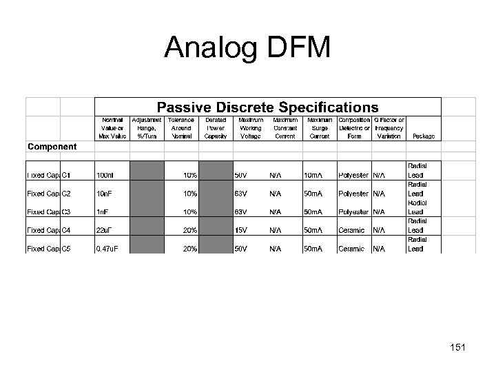 Analog DFM 151
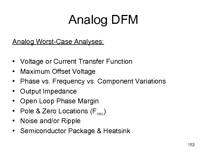 Analog DFM Analog Worst-Case Analyses: • • Voltage or Current Transfer Function Maximum Offset Voltage Phase vs. Frequency vs. Component Variations Output Impedance Open Loop Phase Margin Pole & Zero Locations (Fosc) Noise and/or Ripple Semiconductor Package & Heatsink 152
 Digital DFM DC Drive Analysis Dig Device Output Type Input Type Tech Type DC Drive Device Parameters Vil max Vih min Iil (-) Max Iih max Vol max Voh min Iol max Ioh (-) Min MICRF 005 BM Std N/A N/A 0. 49 V 4. 59 V 5 u. A -5 u. A PIC MPU Std 0. 98 V 4. 08 V -1 u. A 25 m. A 0. 6 V 4. 2 V 25 m. A Checked -3 m. A 153
 Indoor Microprocessor and Display Paul Simons 154
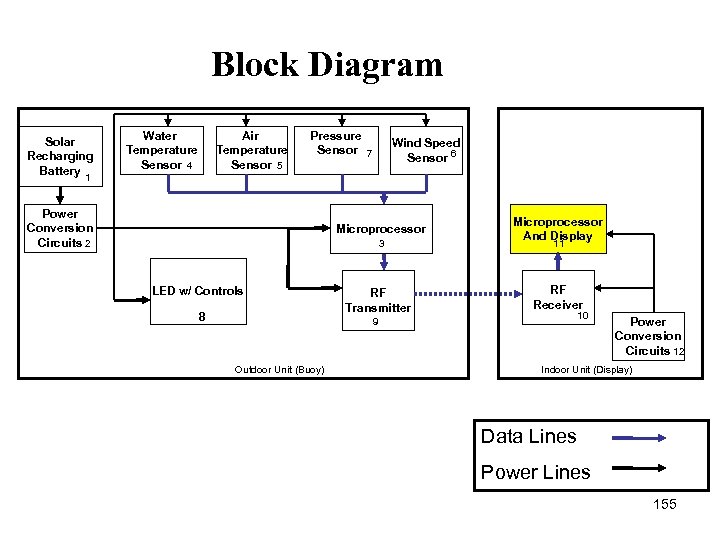 Block Diagram Solar Recharging Battery Water Temperature Sensor 4 Air Temperature Sensor 5 Pressure Sensor 7 Wind Speed Sensor 6 1 Power Conversion Circuits 2 Microprocessor 3 LED w/ Controls 8 RF Transmitter 9 Outdoor Unit (Buoy) Microprocessor And Display 11 RF Receiver 10 Power Conversion Circuits 12 Indoor Unit (Display) Data Lines Power Lines 155
 Functional Purpose • Read digital data out of RF Receiver • Process the results and send digital signal to proper location • Display a visual readout of data 156
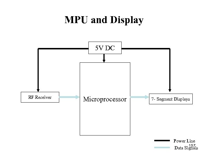 MPU and Display 5 V DC RF Receiver Microprocessor 7 Segment Displays Power Line 157 Data Signals
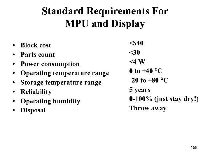 Standard Requirements For MPU and Display • • Block cost Parts count Power consumption Operating temperature range Storage temperature range Reliability Operating humidity Disposal <$40 <30 <4 W 0 to +40 C -20 to +80 C 5 years 0 -100% (just stay dry!) Throw away 158
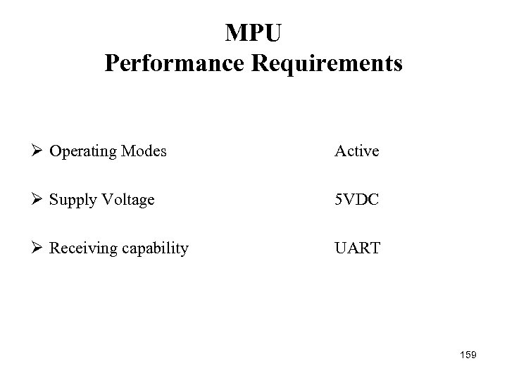 MPU Performance Requirements Ø Operating Modes Active Ø Supply Voltage 5 VDC Ø Receiving capability UART 159
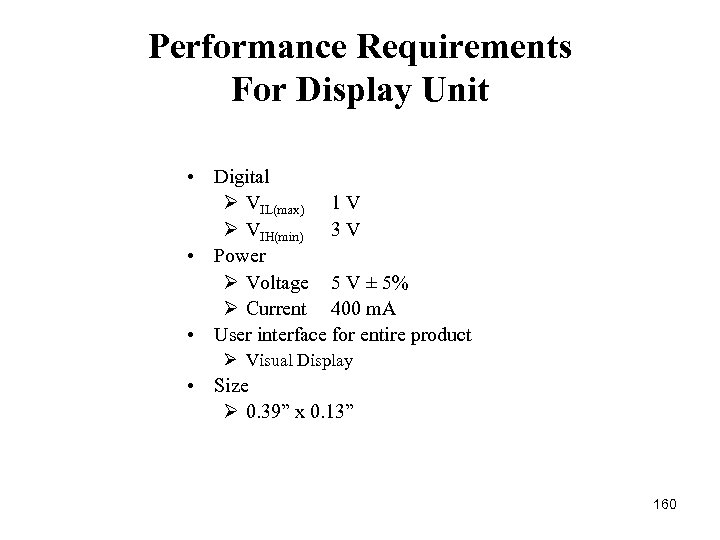 Performance Requirements For Display Unit • Digital Ø VIL(max) 1 V Ø VIH(min) 3 V • Power Ø Voltage 5 V ± 5% Ø Current 400 m. A • User interface for entire product Ø Visual Display • Size Ø 0. 39” x 0. 13” 160
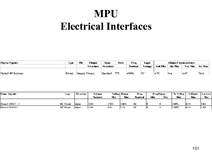 MPU Electrical Interfaces 161
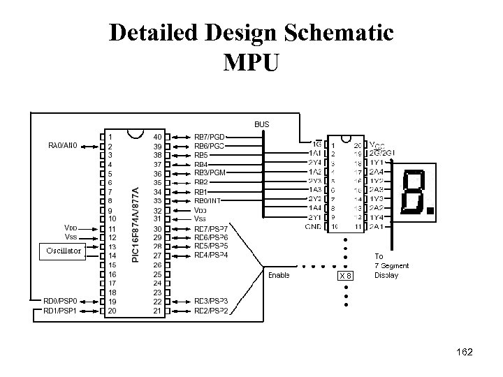 Detailed Design Schematic MPU 162
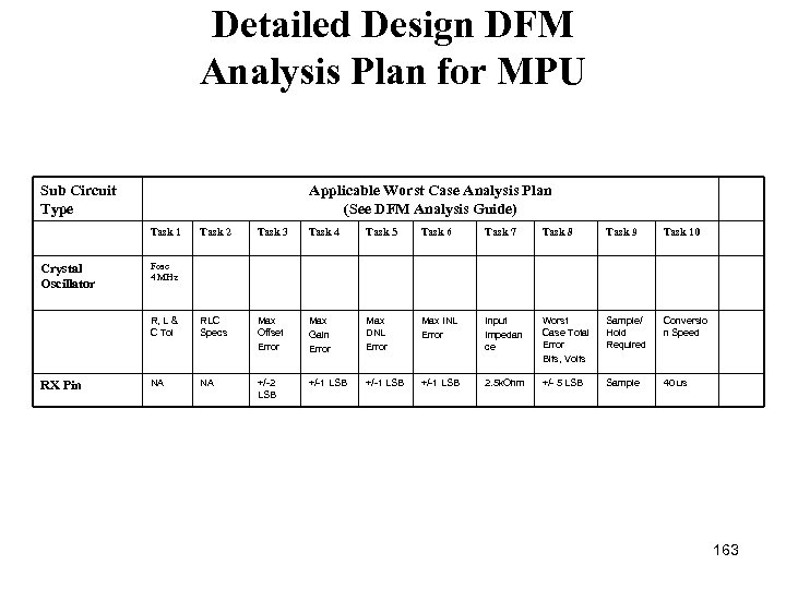 Detailed Design DFM Analysis Plan for MPU Sub Circuit Type Applicable Worst Case Analysis Plan (See DFM Analysis Guide) Task 1 RX Pin Task 3 Task 4 Task 5 Task 6 Task 7 Task 8 Task 9 Task 10 R, L & C Tol Crystal Oscillator Task 2 RLC Specs Max Offset Error Max Gain Error Max DNL Error Max INL Error Input Impedan ce Worst Case Total Error Bits, Volts Sample/ Hold Required Conversio n Speed NA NA +/-2 LSB +/-1 LSB 2. 5 k. Ohm +/- 5 LSB Sample 40 us Fosc 4 MHz 163
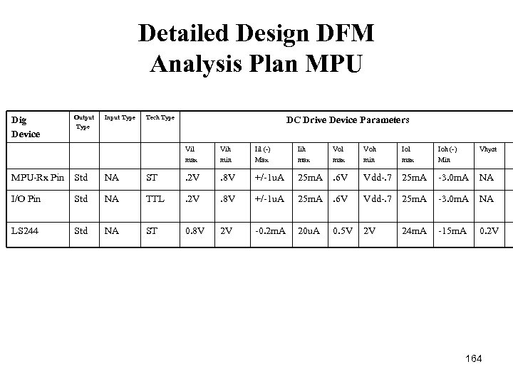 Detailed Design DFM Analysis Plan MPU Dig Device Output Type Input Type Tech Type DC Drive Device Parameters Vil max Vih min Iil ( ) Max Iih max Vol max Voh min Iol max Ioh ( ) Min Vhyst MPU Rx Pin Std NA ST . 2 V . 8 V +/ 1 u. A 25 m. A . 6 V Vdd. 7 25 m. A 3. 0 m. A NA I/O Pin Std NA TTL . 2 V . 8 V +/ 1 u. A 25 m. A . 6 V Vdd. 7 25 m. A 3. 0 m. A NA LS 244 Std NA ST 0. 8 V 2 V 0. 2 m. A 20 u. A 0. 5 V 2 V 24 m. A 15 m. A 0. 2 V 164
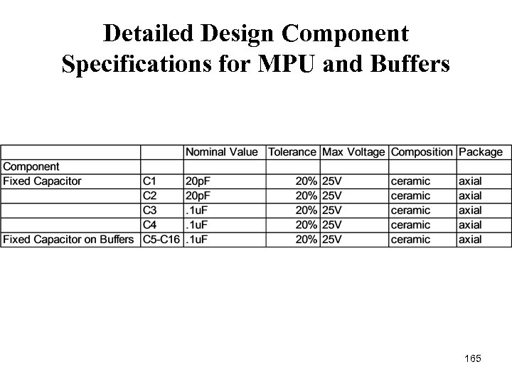 Detailed Design Component Specifications for MPU and Buffers 165
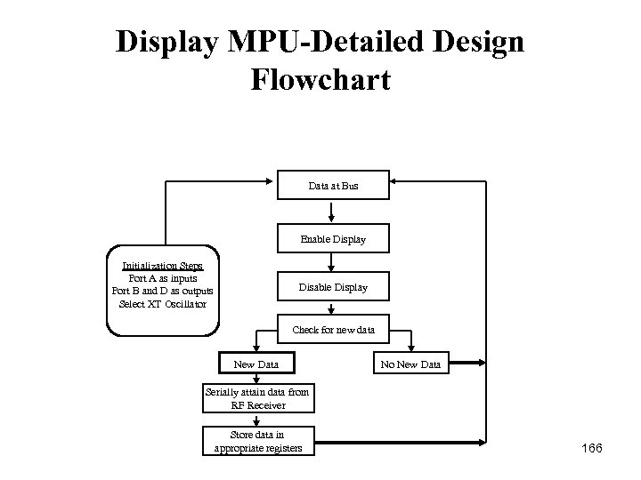 Display MPU-Detailed Design Flowchart Data at Bus Enable Display Initialization Steps Port A as inputs Port B and D as outputs Select XT Oscillator Disable Display Check for new data New Data No New Data Serially attain data from RF Receiver Store data in appropriate registers 166
 MPU-Detailed Design Compatibility of Signals with Transmitter/ Receiver Regulator 4. 9
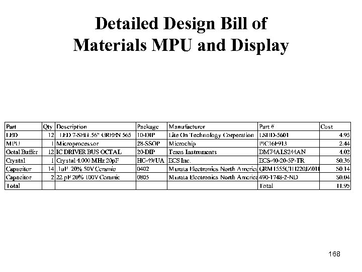 Detailed Design Bill of Materials MPU and Display 168
 Reliability Table 169
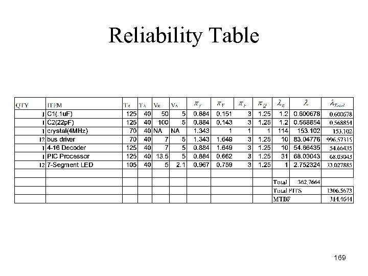
 MPU and Display Summary of Reliability Table • The dominant part for unreliability are the crystal. This is due to the method of approximation used. • To improve this characteristic, a different method of approximation should be used. 170
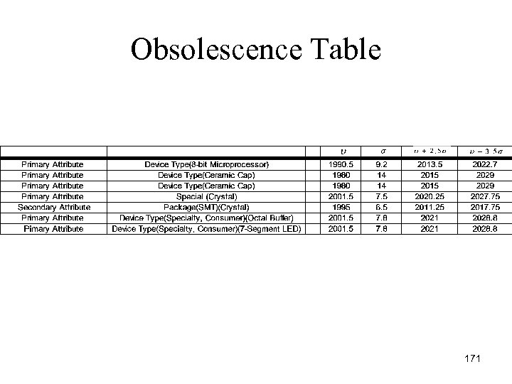 Obsolescence Table 171
 Obsolescence Summary • The worse obsolescence case is 6. 5 years, which is the crystal. However, this exceeds our speculated reliability period of 5 years. 172
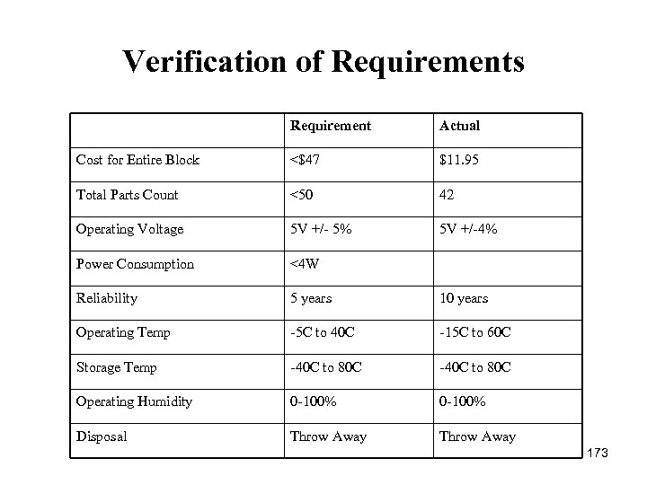 Verification of Requirements Requirement Actual Cost for Entire Block <$47 $11. 95 Total Parts Count <50 42 Operating Voltage 5 V +/ 5% 5 V +/ 4% Power Consumption <4 W Reliability 5 years 10 years Operating Temp 5 C to 40 C 15 C to 60 C Storage Temp 40 C to 80 C Operating Humidity 0 100% Disposal Throw Away 173
 MPU and Display Manufacturing and Testing Requirements • All components reside on PCB #3. • Must test all 7 segment displays to ensure functionality. • Processor must be programmed before soldering onto PCB. • Test entire display unit with RF receiver, MPU, buffers, and displays. 174
 Display Power Regulation Paul Simons Team 3 175
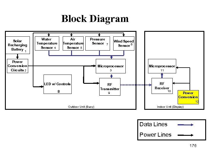 Block Diagram Solar Recharging Battery Water Temperature Sensor 4 Air Temperature Sensor 5 Pressure Sensor 7 Wind Speed Sensor 6 1 Power Conversion Circuits 2 Microprocessor LED w/ Controls 8 Microprocessor 3 11 RF Transmitter 9 RF Receiver 10 Power Conversion 12 Outdoor Unit (Buoy) Indoor Unit (Display) Data Lines Power Lines 176
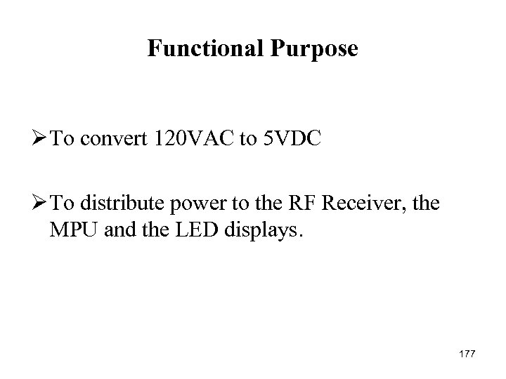 Functional Purpose Ø To convert 120 VAC to 5 VDC Ø To distribute power to the RF Receiver, the MPU and the LED displays. 177
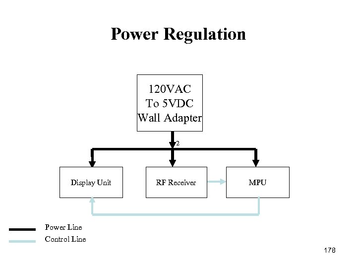 Power Regulation 120 VAC To 5 VDC Wall Adapter 2 Display Unit RF Receiver MPU Power Line Control Line 178
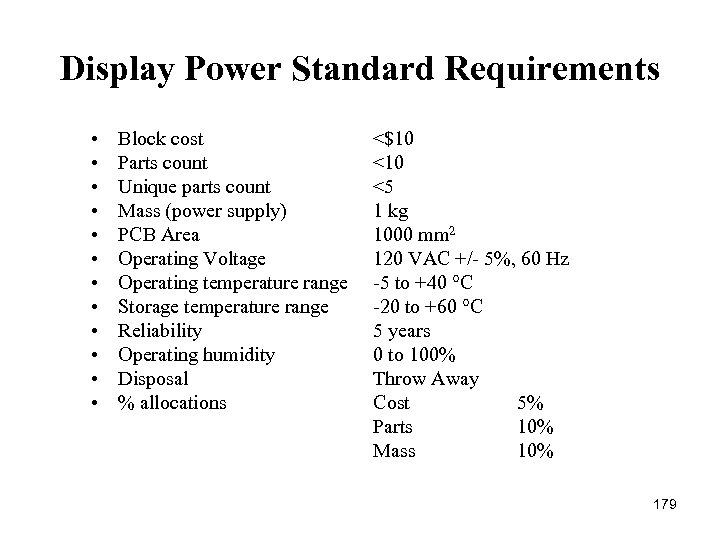 Display Power Standard Requirements • • • Block cost Parts count Unique parts count Mass (power supply) PCB Area Operating Voltage Operating temperature range Storage temperature range Reliability Operating humidity Disposal % allocations <$10 <5 1 kg 1000 mm 2 120 VAC +/ 5%, 60 Hz 5 to +40 C 20 to +60 C 5 years 0 to 100% Throw Away Cost 5% Parts 10% Mass 10% 179
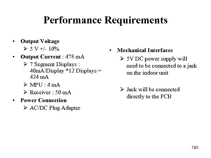 Performance Requirements • Output Voltage Ø 5 V +/ 10% • Output Current : 478 m. A Ø 7 Segment Displays : 40 m. A/Display *12 Displays = 424 m. A Ø MPU : 4 m. A Ø Receiver : 50 m. A • Power Connection Ø AC/DC Plug Adapter • Mechanical Interfaces Ø 5 V DC power supply will need to be connected to a jack on the indoor unit Ø Jack will be connected directly to the PCB 180
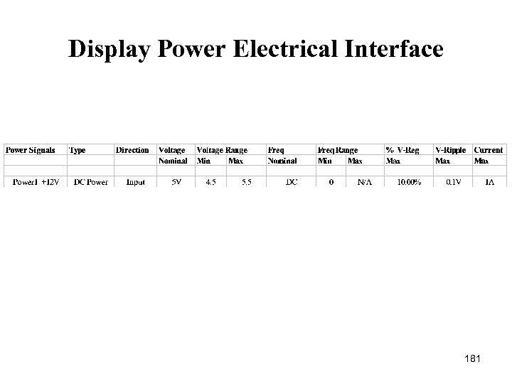 Display Power Electrical Interface 181
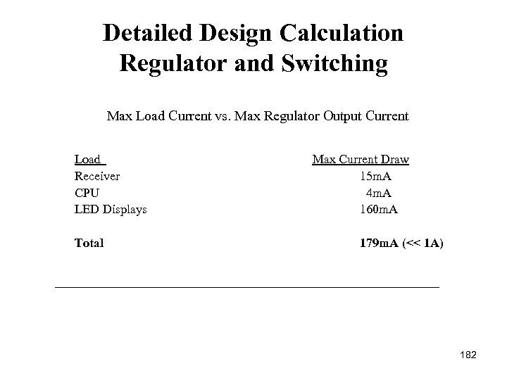 Detailed Design Calculation Regulator and Switching Max Load Current vs. Max Regulator Output Current Load Receiver CPU LED Displays Total Max Current Draw 15 m. A 4 m. A 160 m. A 179 m. A (<< 1 A) 182
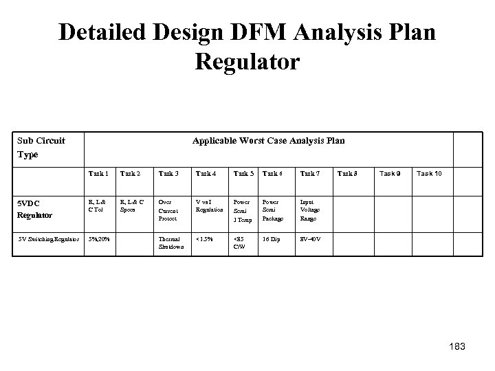 Detailed Design DFM Analysis Plan Regulator Sub Circuit Type Applicable Worst Case Analysis Plan Task 1 Task 2 Task 3 Task 4 Task 5 Task 6 Task 7 5 VDC Regulator R, L & C Tol R, L & C Specs Over Current Protect V vs I Regulation Power Semi J Temp Power Semi Package 5%, 20% Thermal Shutdown <1. 5% <85 C/W 16 Dip Task 9 Task 10 Input Voltage Range 5 V Switching Regulator Task 8 8 V 40 V 183
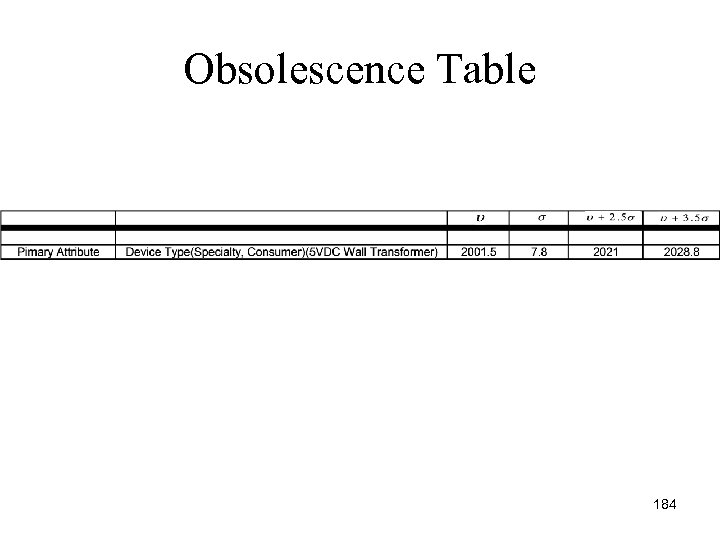 Obsolescence Table 184
 Obsolescence Summary • The worse obsolescence case is 7. 8 years for the wall transformer. However, this exceeds our speculated reliability period of 5 years. 185
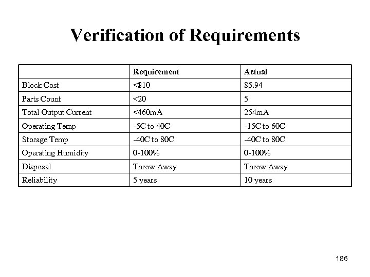 Verification of Requirements Requirement Actual Block Cost <$10 $5. 94 Parts Count <20 5 Total Output Current <460 m. A 254 m. A Operating Temp 5 C to 40 C 15 C to 60 C Storage Temp 40 C to 80 C Operating Humidity 0 100% Disposal Throw Away Reliability 5 years 10 years 186
 Display Power Assembly and Testing • Test to ensure 5 V output. • Solder leads from wall transformer to PCB. 187
 Assembly Level • Level 1: – Program PIC Microcontrollers – Test PIC functionality • Level 2: – Assemble components on PCB 1 (Buoy) and solder – Assemble components on PCB 2 (Buoy) and solder – Assemble components on PCB 3 (Display) and solder 188
 Assembly Level • Level 3: – Construct buoy – Mount battery in the buoy – Mount PCB in the buoy – Mount sensors on buoy externally – Mount antenna on buoy externally – Mount Solar Panel and connect to battery 189
 Assembly Level • Level 4: – Mount PCB in display casing • Level 5: – Perform all necessary functionality tests – Seal buoy and display cases • Level 6: – Place buoy and display module in packaging with user manual. 190
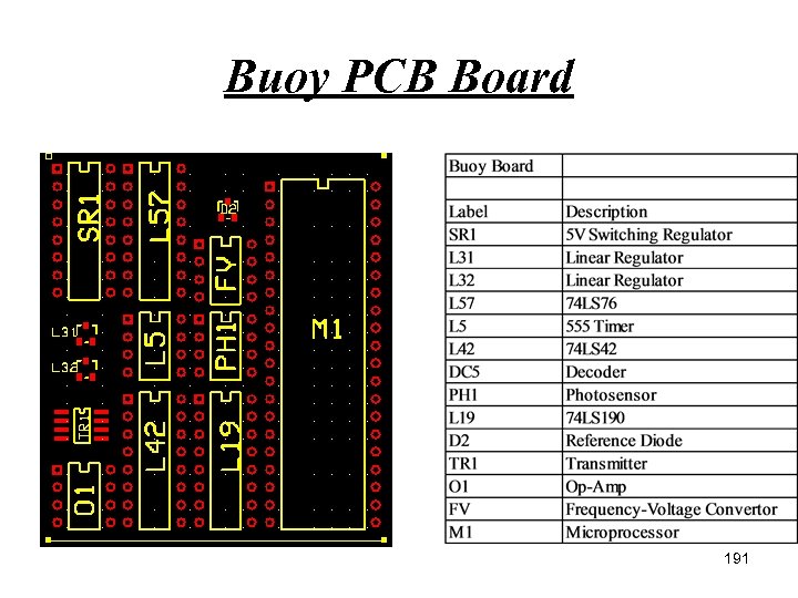 Buoy PCB Board 191
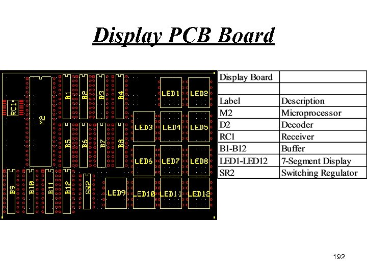 Display PCB Board 192
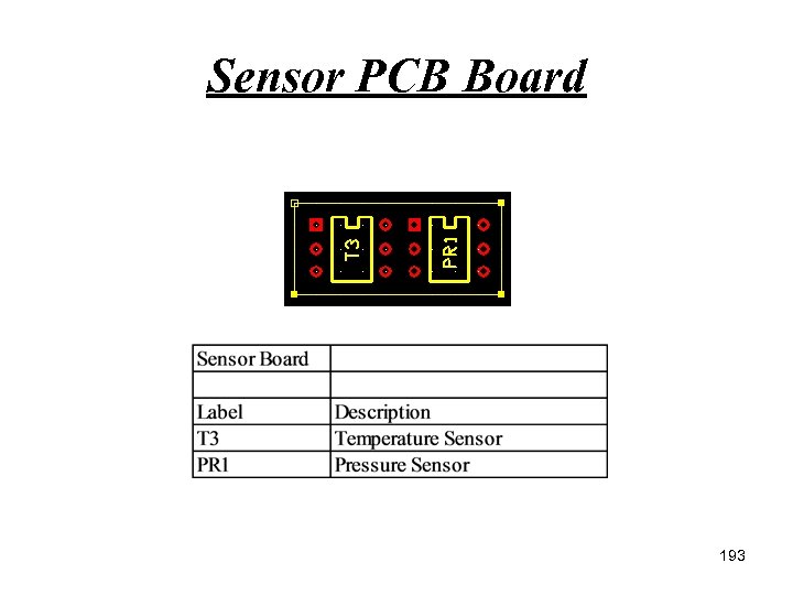 Sensor PCB Board 193
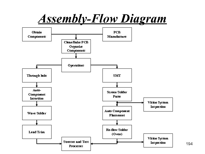 Assembly-Flow Diagram Obtain Components PCB Manufacture Clean/Bake PCB Organize Components Operations Through hole SMT Auto. Component Insertion Screen Solder Paste Vision System Inspection Wave Solder Auto Component Placement Lead Trim Re-flow Solder (Oven) Stresses and Test Processes Vision System Inspection 194


