6ec3ad7d200209cf5ca6686662991dd5.ppt
- Количество слайдов: 36
 Dual Damascene using Step and Flash Imprint Lithography Grant Willson Department of Chemical Engineering Department of Chemistry The University of Texas Austin, Texas 78712 http: //willson. cm. utexas. edu
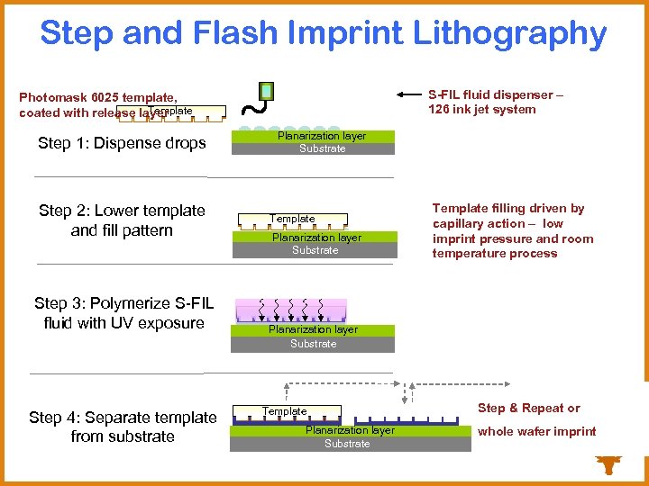 Step and Flash Imprint Lithography S-FIL fluid dispenser – 126 ink jet system Photomask 6025 template, Template coated with release layer Step 1: Dispense drops Step 2: Lower template and fill pattern Step 3: Polymerize S-FIL fluid with UV exposure Step 4: Separate template from substrate Planarization layer Substrate Template filling driven by capillary action – low imprint pressure and room temperature process Planarization layer Substrate Template Planarization layer Substrate Step & Repeat or whole wafer imprint
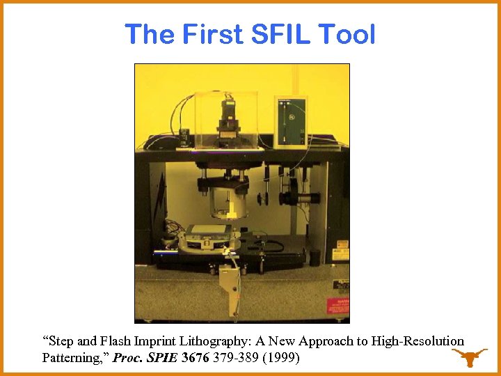 The First SFIL Tool “Step and Flash Imprint Lithography: A New Approach to High-Resolution Patterning, ” Proc. SPIE 3676 379 -389 (1999)
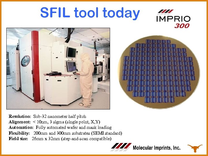 SFIL tool today Resolution: Sub-32 nanometer half pitch Alignment: < 10 nm, 3 sigma (single point, X, Y) Automation: Fully automated wafer and mask loading Flexibility: 200 mm and 300 mm substrates (SEMI standard) Field size: 26 mm x 32 mm (step-and-scan compatible)
 Resolution of Imprint Lithography 2 nm Replication (Rogers et al, Illinois) SFIL 20 nm Replication 25 nm vias ~130 atoms wide 22 nm logic (M 1)
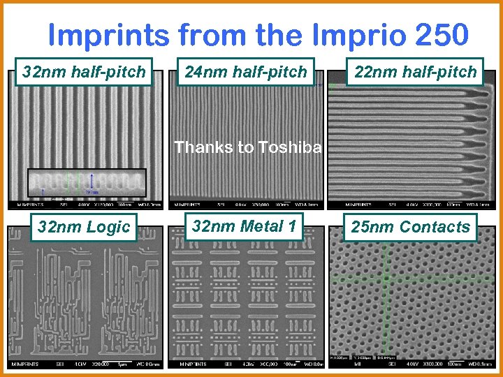 Imprints from the Imprio 250 32 nm half-pitch 24 nm half-pitch 22 nm half-pitch Thanks to Toshiba 32 nm Logic 32 nm Metal 1 25 nm Contacts
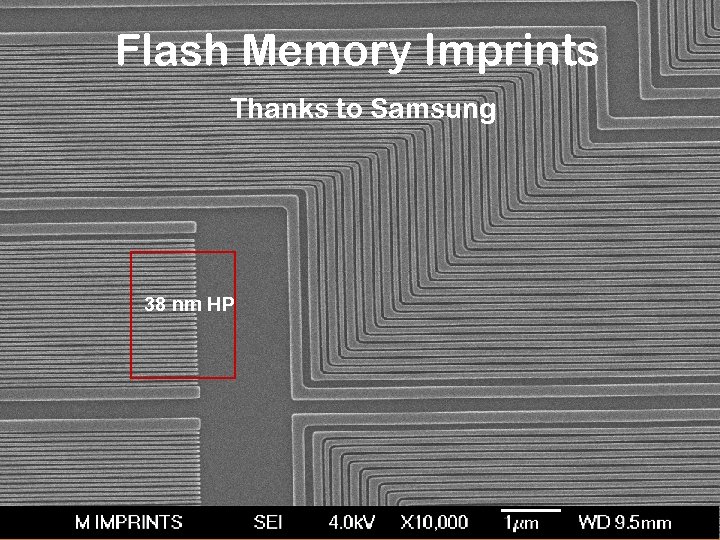 Flash Memory Imprints Thanks to Samsung 38 nm HP
 Non-CMOS Applications 100 nm 20 nm Patterned Photonic Crystals Media
 Multitiered Templates Fabricated with alternating layers of ITO and PECVD Oxide SFIL Imprint S. Johnson, et. al. Microelectron. Eng. (2003) 67, 221
 Our Job! Moore You?
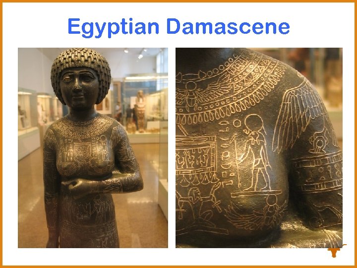 Egyptian Damascene
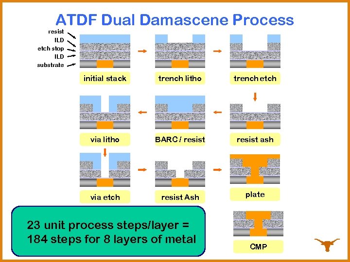 ATDF Dual Damascene Process resist ILD etch stop ILD substrate initial stack trench litho trench etch via litho BARC / resist ash via etch resist Ash plate 23 unit process steps/layer = 184 steps for 8 layers of metal CMP
 Direct Etch or Direct Imprint SIM Process DPD Process Imprint Template SIM Dielectric Layer Previous Metal Layer Imprint Template Sacrificial Imprint Material Directly Patternable Dielectric DPD Previous Metal Layer
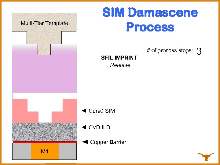 Multi-Tier Template SIM Damascene Process # of process steps: SFIL IMPRINT Release Press Flash ◄ Cured SIM Dispense SIM ◄ CVD ILD Copper Barrier M 1 1 0 3 2
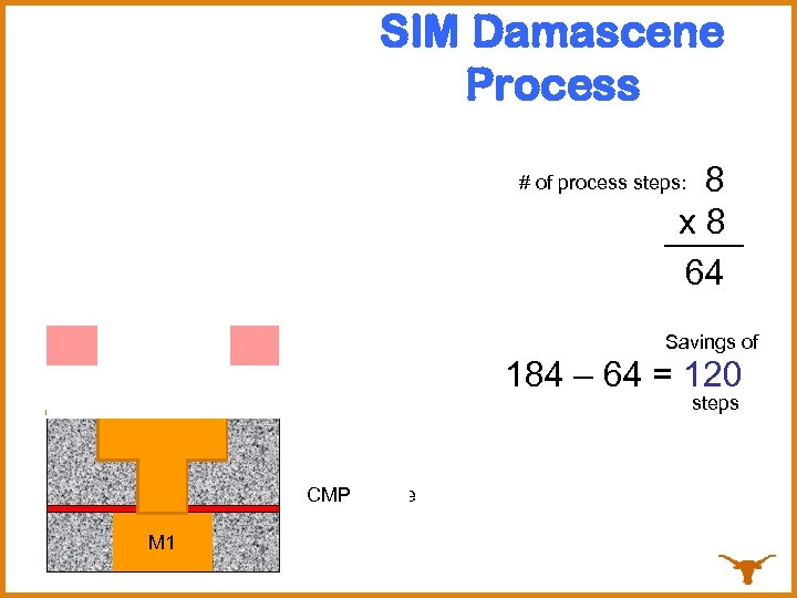 SIM Damascene Process 5 4 6 8 7 3 x 8 64 # of process steps: Savings of 184 – 64 = 120 steps Copper Seed Barrier Etch transfer CMP Plate M 1
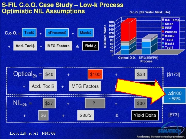
 BEOL Multilevel Imprint Cost Saving 20% l l 20% overall wafer cost saving at 30 wph Cost analysis by Sergei V. Postnikov, Infineon Technologies; presented at Semicon Europa 2007, Stuttgart, Germany
 Lloyd Litt, et. Al NNT 08
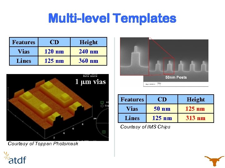 Multi-level Templates Features Vias CD 120 nm Height 240 nm Lines 125 nm 360 nm 1 μm vias Features Vias CD 50 nm Height 125 nm Lines 125 nm 313 nm Courtesy of IMS Chips Courtesy of Toppan Photomask
 Multi-Level S-FIL Test Vehicle Via chain M 1 by M 2 by SFIL Photolithography Test Structures
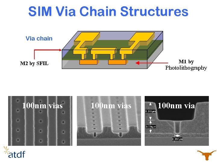 SIM Via Chain Structures Via chain M 1 by M 2 by SFIL 100 nm vias Photolithography 100 nm vias 100 nm via
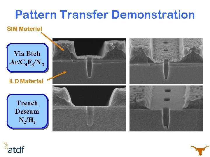 Pattern Transfer Demonstration SIM Material Via Etch Ar/C 4 F 8/N 2 ILD Material Trench Descum N 2/H 2
 Pattern Transfer Demonstration Trench Etch CF 4/C 4 F 8/N 2 Ash N 2/H 2 Both Coral® and Black Diamond® were processed
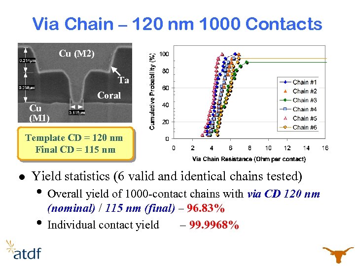 Via Chain – 120 nm 1000 Contacts Cu (M 2) Ta Coral Cu (M 1) Template CD = 120 nm Final CD = 115 nm l Yield statistics (6 valid and identical chains tested) • Overall yield of 1000 -contact chains with via CD 120 nm • (nominal) / 115 nm (final) – 96. 83% Individual contact yield – 99. 9968%
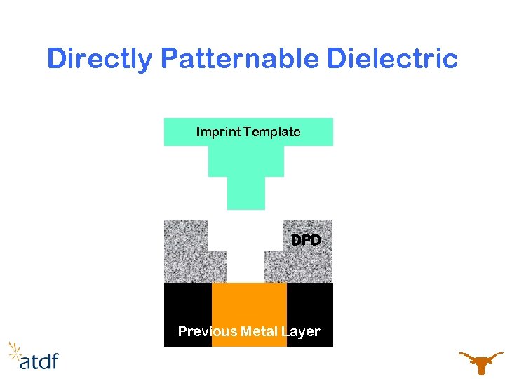 Directly Patternable Dielectric Imprint Template DPD Previous Metal Layer
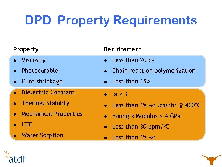 DPD Property Requirements Property Requirement l Viscosity l Less than 20 c. P l Photocurable l Chain reaction polymerization l Cure shrinkage l Less than 15% l Dielectric Constant l l Thermal Stability l Less than 1% wt loss/hr @ 400 o. C l Mechanical Properties l Young’s Modulus ≥ 4 GPa l CTE l Less than 30 ppm/o. C l Water Sorption l Less than 1% wt e≤ 3
 Sol-gel Design/Formulation H 2 O, H+ Alkoxysilanes ultrasonication, vacuum Sol-Gel
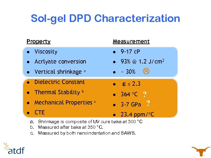 Sol-gel DPD Characterization Property Measurement l Viscosity l 9 -17 c. P l Acrlyate conversion l 93% @ 1. 2 J/cm 2 l Vertical shrinkage a l ~ 30% l Dielectric Constant l l Thermal Stability l l Mechanical Properties l CTE b c e ≤ 2. 3 l ? 3 -7 GPa ? l 23. 4 ppm/°C 364 °C a. Shrinkage is composite of UV cure bake at 300 °C b. Measured after bake at 350 °C. c. Measured by both nanoindentation and SAWS.
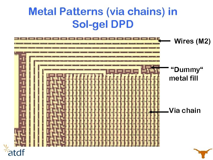 Metal Patterns (via chains) in Sol-gel DPD Wires (M 2) “Dummy“ metal fill Via chain
 Sol-Gel DPD Integration Study BEOL Imprint etch metal CMP uniformity alignment template Defect Sources M 1 defects (not expected) Particle defects (expected)
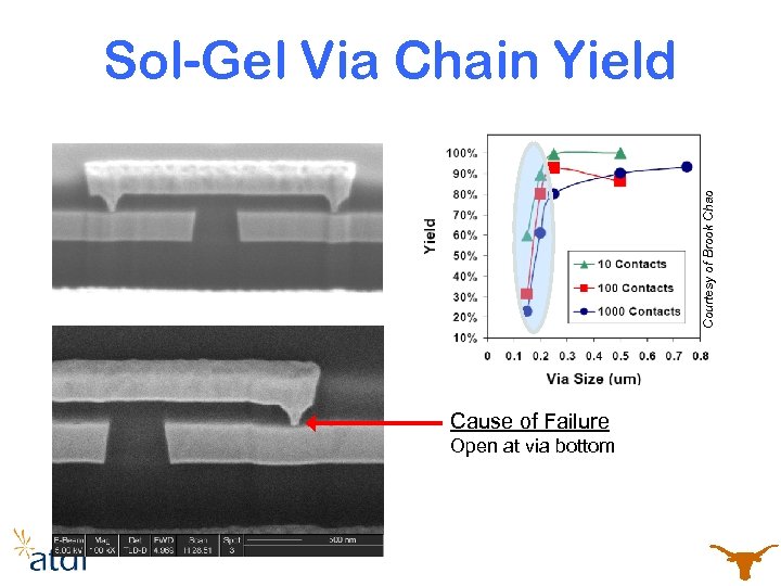 120 nm Via Chains Poor Yield Cause of Failure Open at via bottom Courtesy of Brook Chao Sol-Gel Via Chain Yield
 POSS Design/Synthesis for DPD
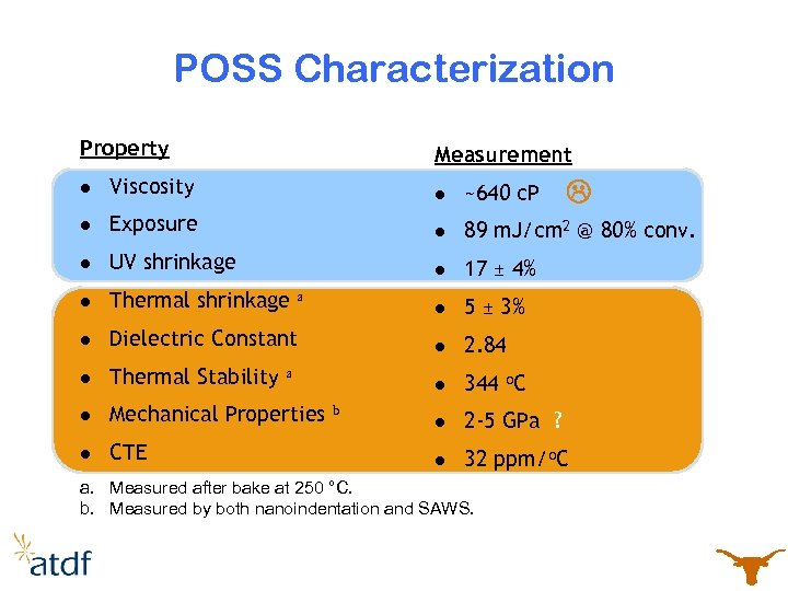 POSS Characterization Property Measurement l Viscosity l ~640 c. P l Exposure l 89 m. J/cm 2 @ 80% conv. l UV shrinkage l 17 ± 4% l Thermal shrinkage l 5 ± 3% l Dielectric Constant l 2. 84 l Thermal Stability l 344 o. C l Mechanical Properties l 2 -5 GPa ? l CTE l 32 ppm/o. C a a b a. Measured after bake at 250 °C. b. Measured by both nanoindentation and SAWS.
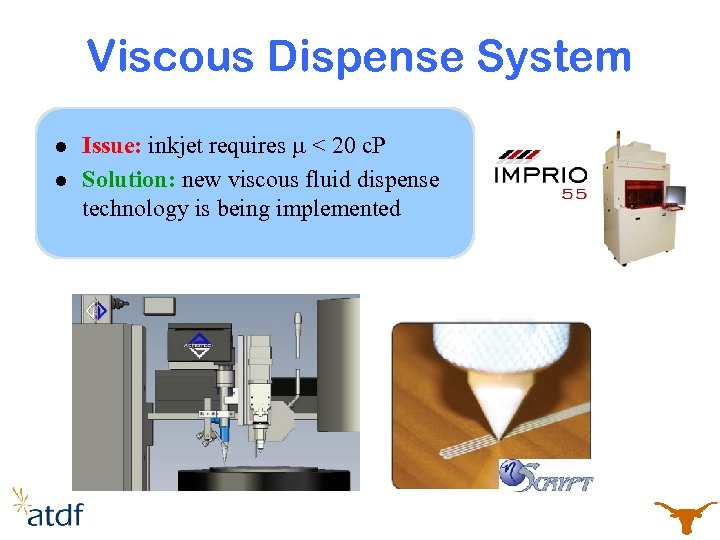 Viscous Dispense System l l Issue: inkjet requires m < 20 c. P Solution: new viscous fluid dispense technology is being implemented
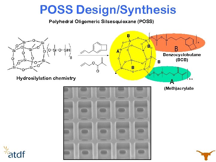 POSS Design/Synthesis Polyhedral Oligomeric Silsesquioxane (POSS) B B A B Benzocyclobutane (BCB) B B Hydrosilylation chemistry A A (Meth)acrylate
 Conclusions l Multi-level S-FIL is a viable approach for Cu / low-k dual damascene processing • SIM Process has been demonstrated by good electrical • yield in various via and line test structures Implementation does not involve reliability testing • Lower cost DPD Process is making progress • Opportunity for materials design • Some processing challenges remain • Implementation of DPD requires reliability testing
 These people did the work Brook H. Chao, Frank Palmieri, Wei-Lun Jen, and D. Hale Mc. Michael The University of Texas at Austin Jordan Owens, Rich Berger, Ken Sotoodeh, Bruce Wilks, Joseph Pham, Ronald Carpio, Ed La. Belle, and Jeff Wetzel Advanced Technology Development Facility, Inc. These people paid for the work


