d247f16fcb9123c4d6e971f3af13a999.ppt
- Количество слайдов: 55
 DTRA Radiation Hardened Microelectronics Program: RH 90 nm Technology Development Program Presented at the Fault Tolerant Space-borne Computing Workshop L. M Cohn/DTRA-RD Lewis. Cohn@DTRA. MIL 28 May 2008
 Agenda • DTRA Radiation Hardened Microelectronics Program • Boeing Radiation Hardening-by-Design (RHBD) 90 nm Program • Radiation Hardening by Process (RHBP) Programs • BAE Systems 90 nm RHBP Program • Honeywell 90 nm RHBP Program • RH Enabling Technology Development Projects • Summary 2
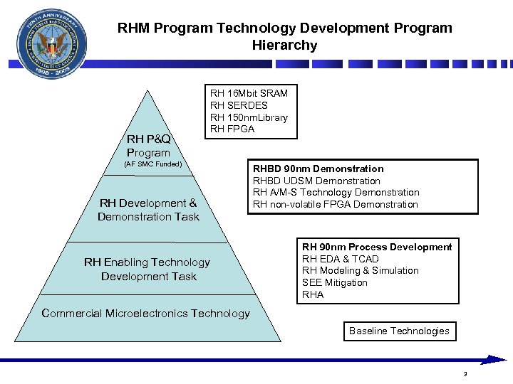 RHM Program Technology Development Program Hierarchy RH P&Q Program RH 16 Mbit SRAM RH SERDES RH 150 nm. Library RH FPGA (AF SMC Funded) RH Development & Demonstration Task RH Enabling Technology Development Task RHBD 90 nm Demonstration RHBD UDSM Demonstration RH A/M-S Technology Demonstration RH non-volatile FPGA Demonstration RH 90 nm Process Development RH EDA & TCAD RH Modeling & Simulation SEE Mitigation RHA Commercial Microelectronics Technology Baseline Technologies 3
 DTRA/DARPA Boeing RHBD 90 nm Program
 RHBD 90 nm Technology Development & Demonstration Program • • Program Objectives Program Description Scope of Work Program Organization Major Accomplishments Technology Transfer Activities Summary 5
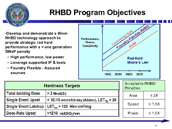 RHBD Program Objectives • Develop and demonstrate a 90 nm RHBD technology approach to provide strategic rad hard performance with a < one generation SWa. P penalty • High performance, low power • Leverage supported IP & tools • Foundry Flexible - Assured sources Hardness Targets Performance, Power, Complexity Acceptable RHBD Penalties Area ≤ 2 X Speed ≤ 1. 5 X Power ≤ 1. 5 X 6
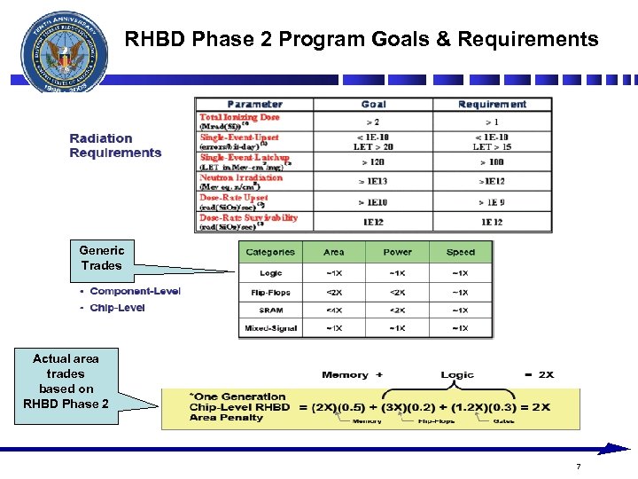 RHBD Phase 2 Program Goals & Requirements Generic Trades Actual area trades based on RHBD Phase 2 7
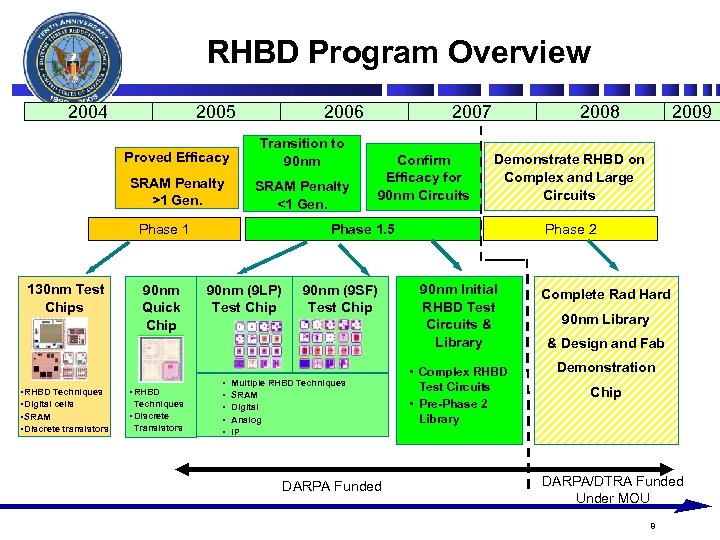 RHBD Program Overview 2004 2005 2006 Proved Efficacy Transition to 90 nm SRAM Penalty >1 Gen. SRAM Penalty <1 Gen. Phase 1 130 nm Test Chips • RHBD Techniques • Digital cells • SRAM • Discrete transistors 90 nm Quick Chip • RHBD Techniques • Discrete Transistors 2007 Confirm Efficacy for 90 nm Circuits 2008 Demonstrate RHBD on Complex and Large Circuits Phase 2 Phase 1. 5 90 nm (9 LP) Test Chip • • • 90 nm (9 SF) Test Chip Multiple RHBD Techniques SRAM Digital Analog IP DARPA Funded 2009 90 nm Initial RHBD Test Circuits & Library Complete Rad Hard • Complex RHBD Test Circuits • Pre-Phase 2 Library Demonstration 90 nm Library & Design and Fab Chip DARPA/DTRA Funded Under MOU 8
 Scope of Work • RHBD Design Techniques Characterization • 90 nm Libraries & IP Development and Optimization • SEE Analysis methods & tools • TCVs, CTVs • PDVs – Demonstrations fabricated and Characterized • TRL “TBD” Design Capability • 65 nm and 45 nm preliminary investigations 9
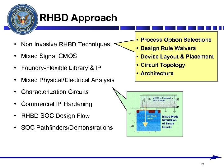 RHBD Approach • Non Invasive RHBD Techniques • Mixed Signal CMOS • Foundry-Flexible Library & IP • Mixed Physical/Electrical Analysis • • • Process Option Selections Design Rule Waivers Device Layout & Placement Circuit Topology Architecture • Characterization Circuits • Commercial IP Hardening • RHBD SOC Design Flow • SOC Pathfinders/Demonstrations 10
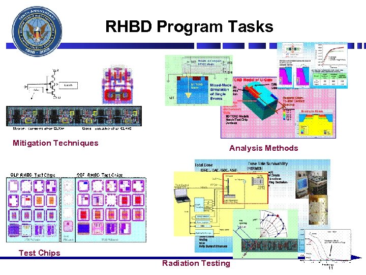 RHBD Program Tasks Mitigation Techniques Analysis Methods Test Chips Radiation Testing 11
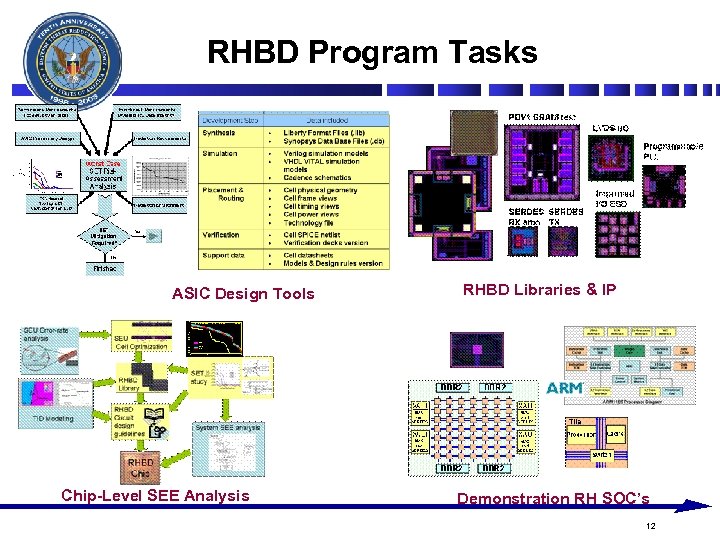 RHBD Program Tasks ASIC Design Tools Chip-Level SEE Analysis RHBD Libraries & IP Demonstration RH SOC’s 12
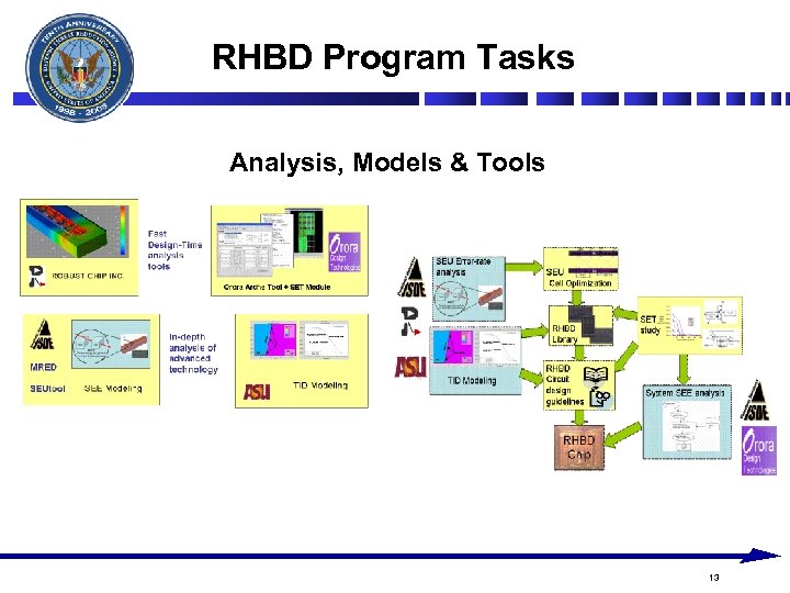 RHBD Program Tasks Analysis, Models & Tools 13
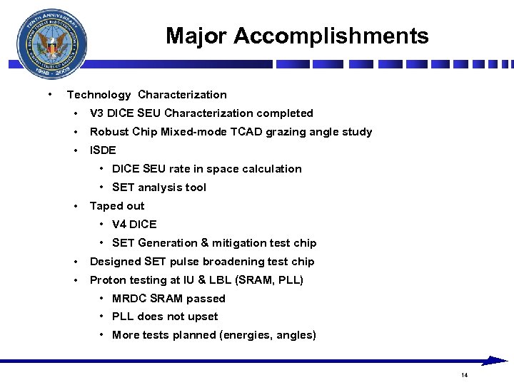 Major Accomplishments • Technology Characterization • V 3 DICE SEU Characterization completed • Robust Chip Mixed-mode TCAD grazing angle study • ISDE • DICE SEU rate in space calculation • SET analysis tool • Taped out • V 4 DICE • SET Generation & mitigation test chip • Designed SET pulse broadening test chip • Proton testing at IU & LBL (SRAM, PLL) • MRDC SRAM passed • PLL does not upset • More tests planned (energies, angles) 14
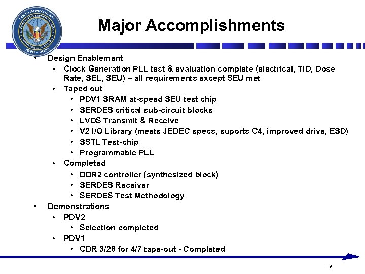 Major Accomplishments • • Design Enablement • Clock Generation PLL test & evaluation complete (electrical, TID, Dose Rate, SEL, SEU) – all requirements except SEU met • Taped out • PDV 1 SRAM at-speed SEU test chip • SERDES critical sub-circuit blocks • LVDS Transmit & Receive • V 2 I/O Library (meets JEDEC specs, suports C 4, improved drive, ESD) • SSTL Test-chip • Programmable PLL • Completed • DDR 2 controller (synthesized block) • SERDES Receiver • SERDES Test Methodology Demonstrations • PDV 2 • Selection completed • PDV 1 • CDR 3/28 for 4/7 tape-out - Completed 15
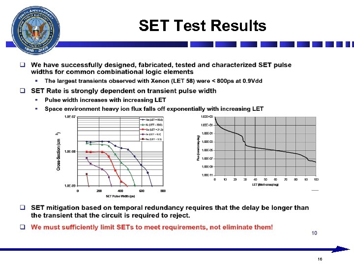 SET Test Results 16
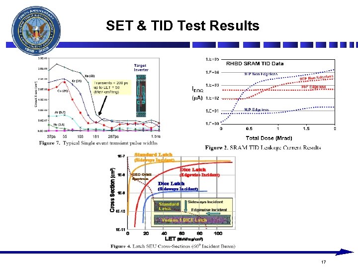 SET & TID Test Results 17
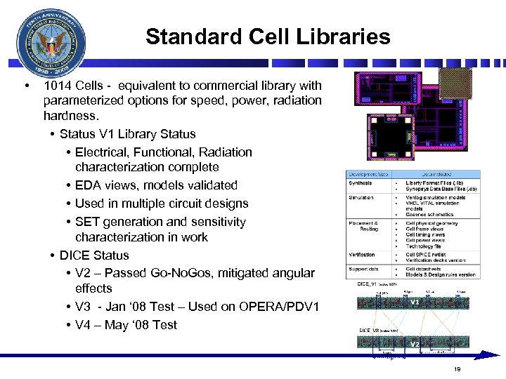 Standard Cell Libraries • 1014 Cells - equivalent to commercial library with parameterized options for speed, power, radiation hardness. • Status V 1 Library Status • Electrical, Functional, Radiation characterization complete • EDA views, models validated • Used in multiple circuit designs • SET generation and sensitivity characterization in work • DICE Status • V 2 – Passed Go-No. Gos, mitigated angular effects • V 3 - Jan ‘ 08 Test – Used on OPERA/PDV 1 • V 4 – May ‘ 08 Test 18
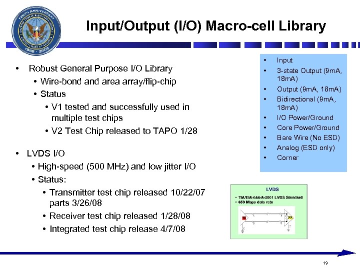 Input/Output (I/O) Macro-cell Library • Robust General Purpose I/O Library • Wire-bond area array/flip-chip • Status • V 1 tested and successfully used in multiple test chips • V 2 Test Chip released to TAPO 1/28 • LVDS I/O • High-speed (500 MHz) and low jitter I/O • Status: • Transmitter test chip released 10/22/07 parts 3/26/08 • Receiver test chip released 1/28/08 • Integrated test chip release 4/7/08 • • • Input 3 -state Output (9 m. A, 18 m. A) Bidirectional (9 m. A, 18 m. A) I/O Power/Ground Core Power/Ground Bare Wire (No ESD) Analog (ESD only) Corner 19
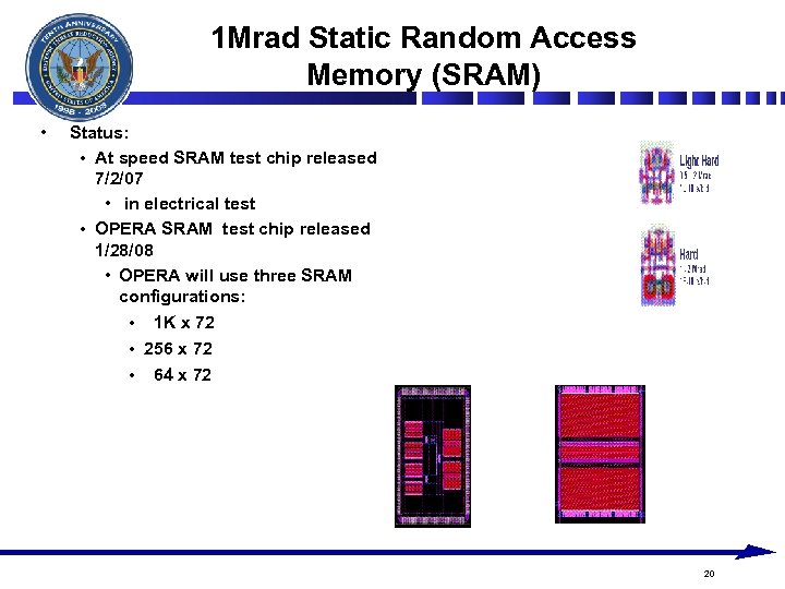 1 Mrad Static Random Access Memory (SRAM) • Status: • At speed SRAM test chip released 7/2/07 • in electrical test • OPERA SRAM test chip released 1/28/08 • OPERA will use three SRAM configurations: • 1 K x 72 • 256 x 72 • 64 x 72 20
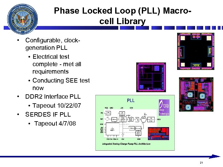 Phase Locked Loop (PLL) Macrocell Library • Configurable, clockgeneration PLL • Electrical test complete - met all requirements • Conducting SEE test now • DDR 2 Interface PLL • Tapeout 10/22/07 • SERDES IF PLL • Tapeout 4/7/08 21
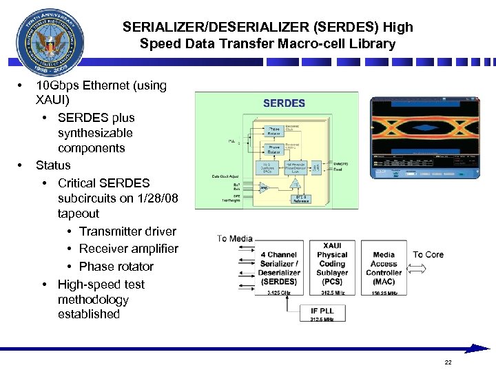 SERIALIZER/DESERIALIZER (SERDES) High Speed Data Transfer Macro-cell Library • • 10 Gbps Ethernet (using XAUI) • SERDES plus synthesizable components Status • Critical SERDES subcircuits on 1/28/08 tapeout • Transmitter driver • Receiver amplifier • Phase rotator • High-speed test methodology established 22
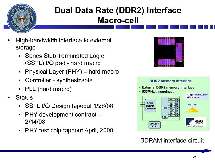 Dual Data Rate (DDR 2) Interface Macro-cell • High-bandwidth interface to external storage • Series Stub Terminated Logic (SSTL) I/O pad - hard macro • Physical Layer (PHY) – hard macro • Controller - synthesizable • PLL (hard macro) • Status • SSTL I/O Design tapeout 1/28/08 • PHY development contract – 2/14/08 • PHY test chip tapeout April, 2008 SDRAM interface circuit 23
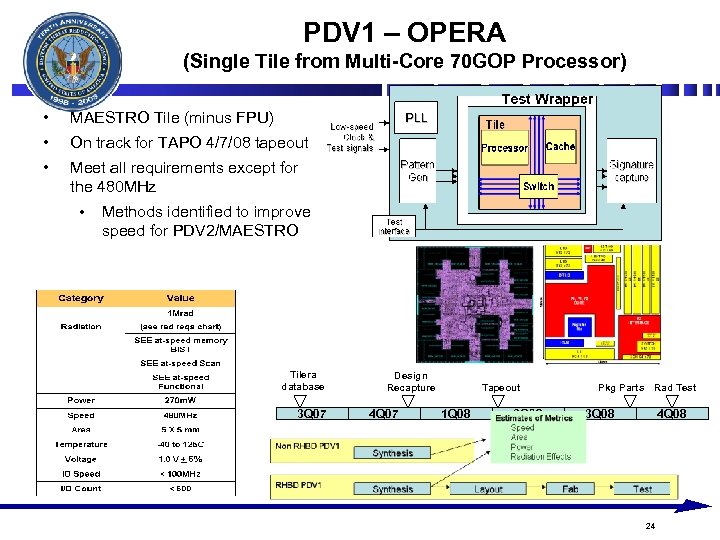 PDV 1 – OPERA (Single Tile from Multi-Core 70 GOP Processor) • MAESTRO Tile (minus FPU) • On track for TAPO 4/7/08 tapeout • Meet all requirements except for the 480 MHz • Methods identified to improve speed for PDV 2/MAESTRO Tilera database 3 Q 07 Design Recapture 4 Q 07 Tapeout 1 Q 08 2 Q 08 Pkg Parts Rad Test 3 Q 08 4 Q 08 24
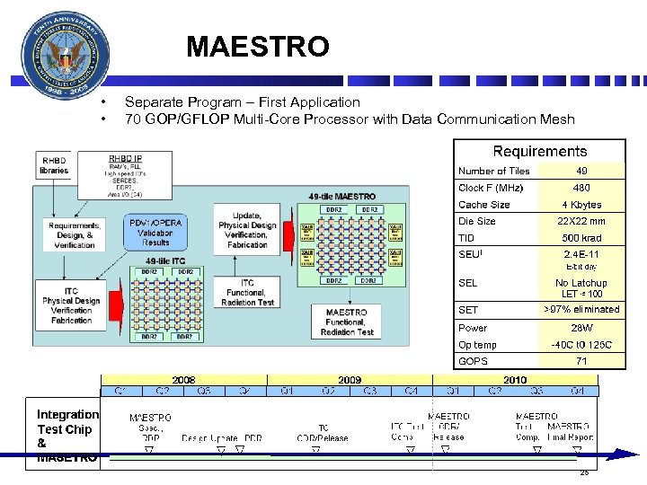 MAESTRO • • Separate Program – First Application 70 GOP/GFLOP Multi-Core Processor with Data Communication Mesh 25
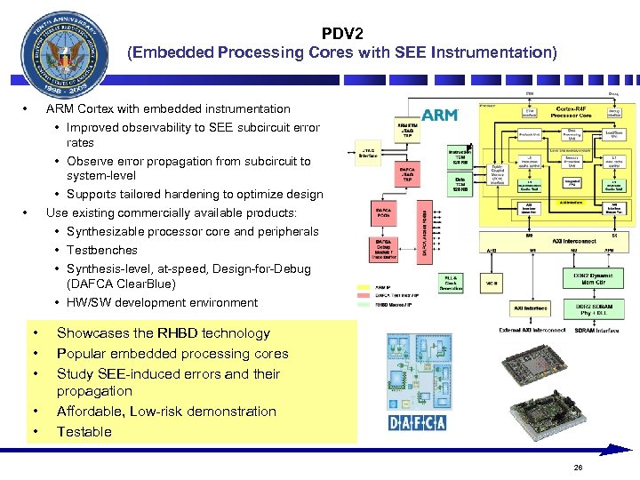 PDV 2 (Embedded Processing Cores with SEE Instrumentation) • ARM Cortex with embedded instrumentation • • Improved observability to SEE subcircuit error rates • Observe error propagation from subcircuit to system-level • Supports tailored hardening to optimize design Use existing commercially available products: • Synthesizable processor core and peripherals • Testbenches • Synthesis-level, at-speed, Design-for-Debug (DAFCA Clear. Blue) • HW/SW development environment • • • Showcases the RHBD technology Popular embedded processing cores Study SEE-induced errors and their propagation Affordable, Low-risk demonstration Testable 26
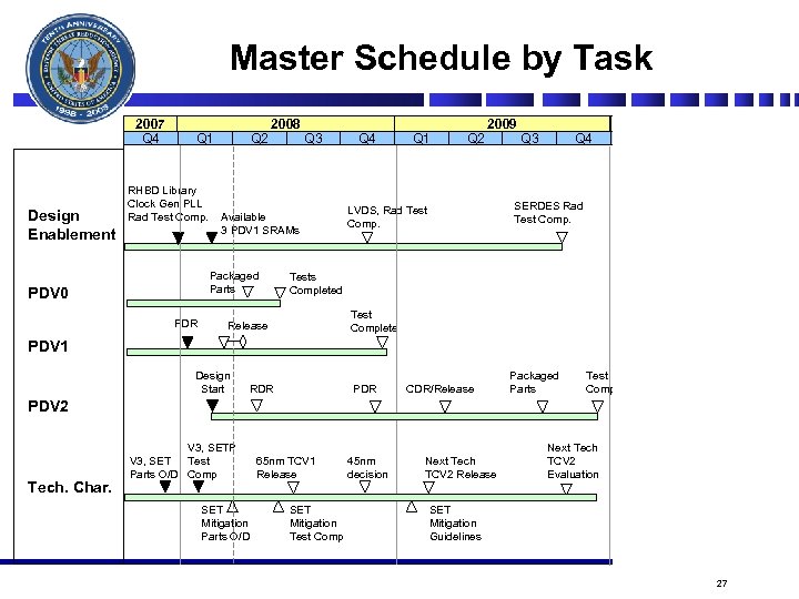 Master Schedule by Task 2007 Q 4 Design Enablement Q 1 RHBD Library Clock Gen PLL Rad Test Comp. Q 2 2008 Available 3 PDV 1 SRAMs Packaged Parts PDV 0 PDR Q 3 Q 4 Q 1 Q 2 2009 Q 3 Q 4 Q 1 2010 Q 2 Q 3 SERDES Rad Test Comp. LVDS, Rad Test Comp. Tests Completed Test Complete Release PDV 1 Design Start PDR RDR CDR/Release Packaged Parts Test Comp. PDV 2 Tech. Char. V 3, SETP V 3, SET Test Parts O/D Comp SET Mitigation Parts O/D 65 nm TCV 1 Release SET Mitigation Test Comp 45 nm decision Next Tech TCV 2 Release Next Tech TCV 2 Evaluation SET Mitigation Guidelines 27
 Technology Transfer Activities • The DTRA/Boeing technology development programs, starting in 1996, have had a strong focus on technology transfer. • • • Focusing on the RHBD Phase 2 Program technology transfer activities include: • • • RH Digital Signal Processor Foundry Independent RH Microelectronics RH EDA Very Deep Submicron Microelectronics RH EDA Ultra-Deep Submicron Microelectronics Development of this capability at the Boeing “Phantom Works” to serve the entire DOD and commercial satellite and missile system community; N. B. this organization serves as a “pure play” design house with many customers outside of Boeing. Direct transfer to the AF TSAT SPO & Boeing TSAT Program Office WRT Single-Event Effects mitigation at 90 nm – In progress and mitigation methods incorporated into Boeing design. Direct support of three OGA Programs; 96 GFLOP DSP and the Opera & Maestro microprocessor architectures – In progress, see PDV-1 discussion. Wide dissemination of the ongoing technology development efforts through briefings at NSREC, HEART, GOMAC, Aerospace Conference and other speaking venues. Significant program review attendance by AF SMC, Aerospace Corp. , DARPA, Boeing Space Systems, GD, and others. Bottom Line: The government owns this technology and will ensure that it is made available to any and all government contractors and both Boeing and DARPA concur with this position. 28
 Summary • RHBD Phase 2 program is on schedule to demonstrate a RHBD 90 nm general purpose microprocessor structure identified “Opera” by June 2008 • Design of Opera previously accomplished through DARPA, USAF & OGA polymorphic computing program) • RHBD digital 90 nm libraries have been demonstrated • Additional macro-cells to complete the demonstration are in development and on schedule • The overall program is on schedule (all technical requirements, cost and schedule on track). • The cell library and macro-cells are owned by the government and available to other government organizations and their contractors 29
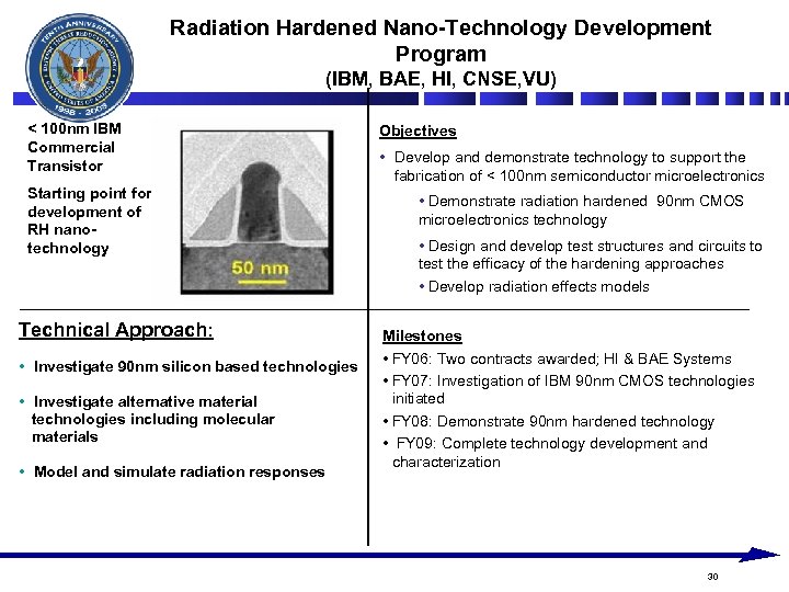 Radiation Hardened Nano-Technology Development Program (IBM, BAE, HI, CNSE, VU) < 100 nm IBM Commercial Transistor Starting point for development of RH nanotechnology Technical Approach: • Investigate 90 nm silicon based technologies • Investigate alternative material technologies including molecular materials • Model and simulate radiation responses Objectives • Develop and demonstrate technology to support the fabrication of < 100 nm semiconductor microelectronics • Demonstrate radiation hardened 90 nm CMOS microelectronics technology • Design and develop test structures and circuits to test the efficacy of the hardening approaches • Develop radiation effects models Milestones • FY 06: Two contracts awarded; HI & BAE Systems • FY 07: Investigation of IBM 90 nm CMOS technologies initiated • FY 08: Demonstrate 90 nm hardened technology • FY 09: Complete technology development and characterization 30
 BAE Systems RH 90 nm Program
 BAE Systems RH 90 nm Program • • Program Description Goals and Requirements Technical Approach Major Accomplishments • Testing and Simulation Results • Technology Transfer • Summary 32
 Program Description: Evaluation of 90 nm commercial bulk CMOS technology and initial development of 90 nm Rad Hard techniques Customer: Defense Threat Reduction Agency (DTRA) Period of Performance: 3/31/06 to 8/31/09 Teammates/Subcontractors: IBM and Vanderbilt University Collaborators: CNSE, NRL, AFRL, TAPO Program Objectives: • Radiation Hardness evaluation of existing 90 nm test structures • Design of Experiments (DOE) of minimally invasive RH techniques • Design/Fabrication/Evaluation of Technology Characterization Vehicle (TCV) 33
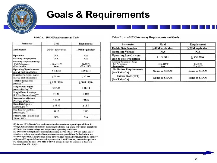 Goals & Requirements 34
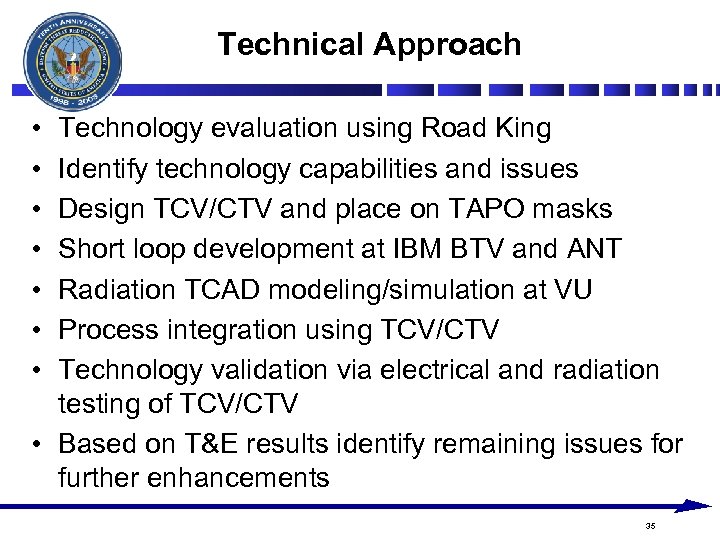 Technical Approach • • Technology evaluation using Road King Identify technology capabilities and issues Design TCV/CTV and place on TAPO masks Short loop development at IBM BTV and ANT Radiation TCAD modeling/simulation at VU Process integration using TCV/CTV Technology validation via electrical and radiation testing of TCV/CTV • Based on T&E results identify remaining issues for further enhancements 35
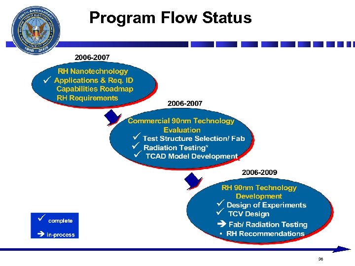 Program Flow Status 36
 Major Accomplishments • Baseline technology radiation testing and characterization completed • Completed base SEU 3 D mixed mode simulations on the 2. 3 um 2 memory cell; results shows ample SEU hardness margin with targeted R and C • Radiation testing on test structures completed • Total ionizing dose • Single Event Gate Rupture • Single Event Upset • SRAM cell design completed • TCV designed completed and fabrication initiated 37
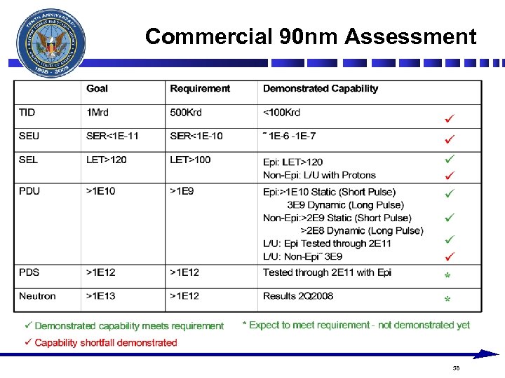 Commercial 90 nm Assessment 38
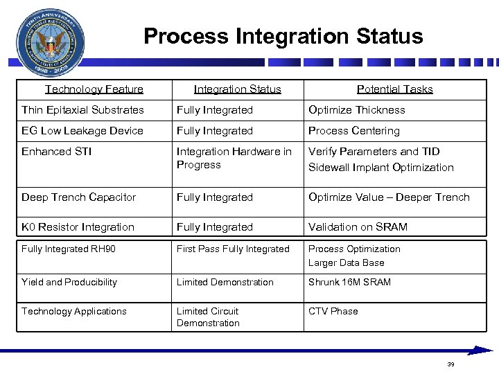 Process Integration Status Technology Feature Integration Status Potential Tasks Thin Epitaxial Substrates Fully Integrated Optimize Thickness EG Low Leakage Device Fully Integrated Process Centering Enhanced STI Integration Hardware in Progress Verify Parameters and TID Sidewall Implant Optimization Deep Trench Capacitor Fully Integrated Optimize Value – Deeper Trench K 0 Resistor Integration Fully Integrated Validation on SRAM Fully Integrated RH 90 First Pass Fully Integrated Process Optimization Larger Data Base Yield and Producibility Limited Demonstration Shrunk 16 M SRAM Technology Applications Limited Circuit Demonstration CTV Phase 39
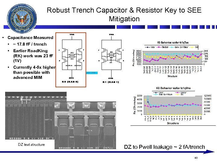 Robust Trench Capacitor & Resistor Key to SEE Mitigation • Capacitance Measured • ~ 17. 8 f. F / trench • Earlier Road. King (RK) work was 23 f. F (1 V) • Currently 4 -5 x higher than possible with advanced MIM DZ test structure DZ to Pwell leakage ~ 2 f. A/trench 40
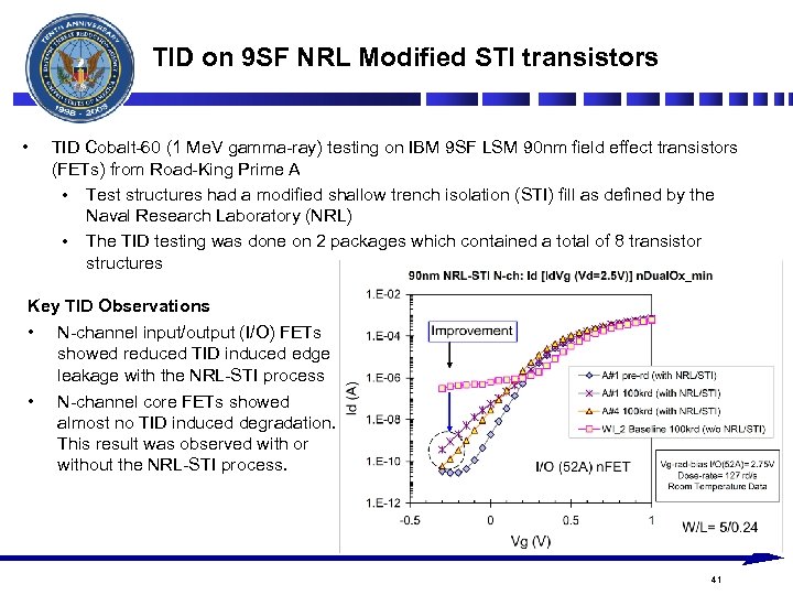 TID on 9 SF NRL Modified STI transistors • TID Cobalt-60 (1 Me. V gamma-ray) testing on IBM 9 SF LSM 90 nm field effect transistors (FETs) from Road-King Prime A • Test structures had a modified shallow trench isolation (STI) fill as defined by the Naval Research Laboratory (NRL) • The TID testing was done on 2 packages which contained a total of 8 transistor structures Key TID Observations • N-channel input/output (I/O) FETs showed reduced TID induced edge leakage with the NRL-STI process • N-channel core FETs showed almost no TID induced degradation. This result was observed with or without the NRL-STI process. 41
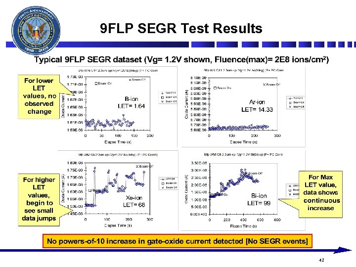 9 FLP SEGR Test Results 42
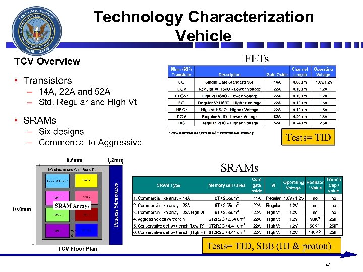 Technology Characterization Vehicle 43
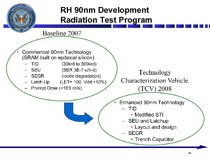 RH 90 nm Development Radiation Test Program 44
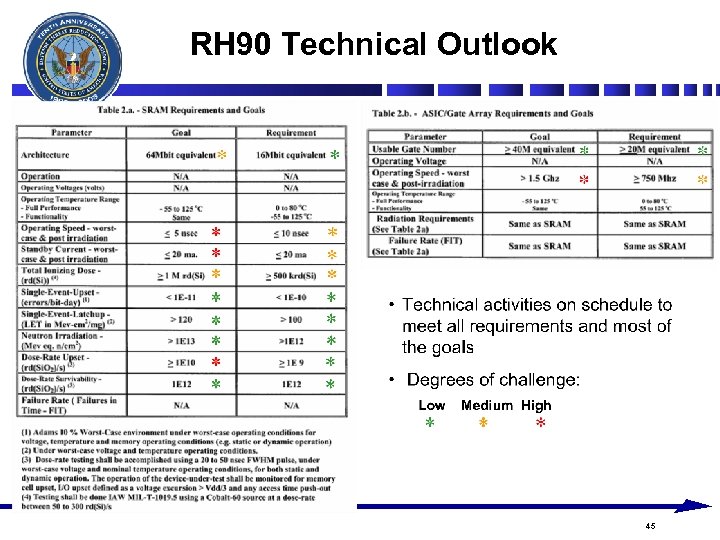 RH 90 Technical Outlook 45
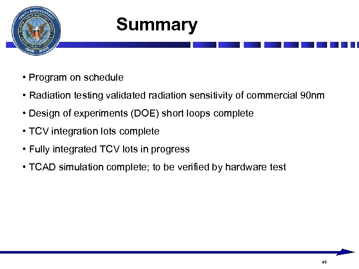 Summary • Program on schedule • Radiation testing validated radiation sensitivity of commercial 90 nm • Design of experiments (DOE) short loops complete • TCV integration lots complete • Fully integrated TCV lots in progress • TCAD simulation complete; to be verified by hardware test 46
 Honeywell RH 90 nm Program
 Honeywell SSED RH 90 nm Program • • • Program Objectives Major Accomplishments Technology Development Status Schedule Summary 48
 Program Objectives • Objectives of the program • Design, fabricate, test and evaluate nanotechnology test structures and circuits to support radiation testing and characterization • Characterize and project the radiation response of those identified technologies • Develop radiation hardening technology suitable to support the demonstration of RH nanotechnology devices and circuits 49
 Honeywell / IBM Collaboration • Honeywell has teamed with IBM to develop a 90 nm rad-hard SOI technology • Based on IBM’s 90 nm SOI technology, with Honeywell’s radiation hardening technology added • Multiple Vt’s, single core gate oxide, 63 nm Lpoly, body tied • 10 LM • Low k Copper BEOL • Deep trench capacitor and IP • Ta. N resistor • First phase will demonstrate all key modules necessary to achieve the desired SRAM cell size and have the devices needed for SER hardening 50
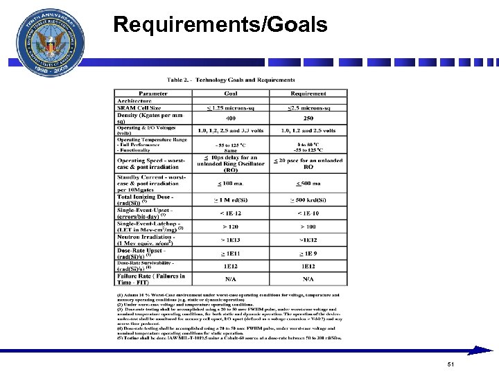 Requirements/Goals 51
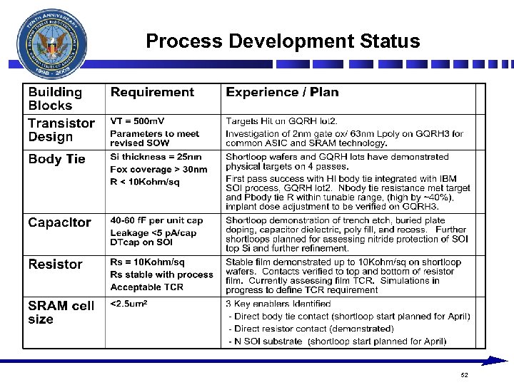 Process Development Status 52
 RH Enabling Technology Development Projects
 Enabling Technology Development Project Contributors • • ASU CFDRC Lynguent MRDC Orora RAD Robust Chip, Inc. Vanderbilt University 55
 RH 90 nm Technology Development and Demonstration Program Summary • The DTRA RHM Program is pursuing the development and demonstration of RH 90 nm technology through two basic approaches: • A Joint RHBD project with DARPA with Boeing/IBM • Two RHBP technology development efforts with BAE/IBM and Honeywell/IBM • RHBD project is on schedule to test and characterize two PDV devices by 4 QCY 2009. • RHBP efforts are scheduled to demonstrate an integrated RH 90 nm process by 2009 • Follow-on program required to demonstrate a RHBP PDV. • In addition, a number of enabling technology projects are underway to address specific issues such as SEE and radiation response modeling and characterization. 56


