c416034449aab8f61a87cddec453f153.ppt
- Количество слайдов: 79
 Digital Logic Synthesis for Memristors
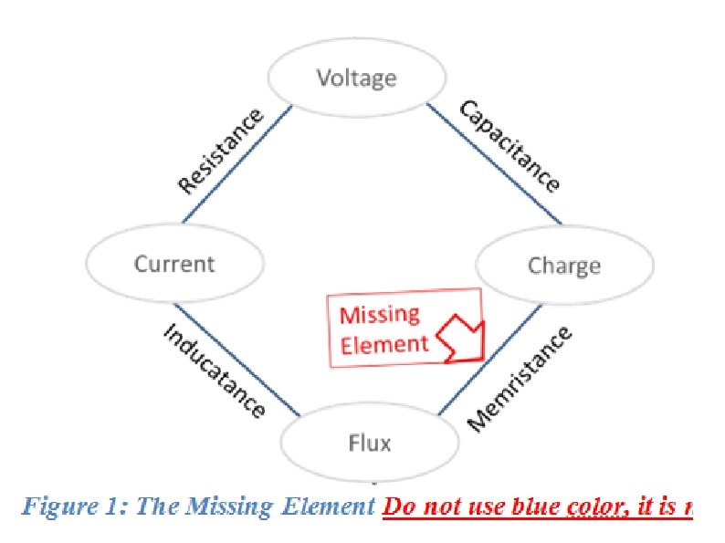
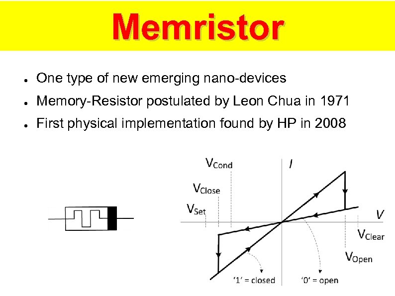 Memristor ● One type of new emerging nano-devices ● Memory-Resistor postulated by Leon Chua in 1971 ● First physical implementation found by HP in 2008
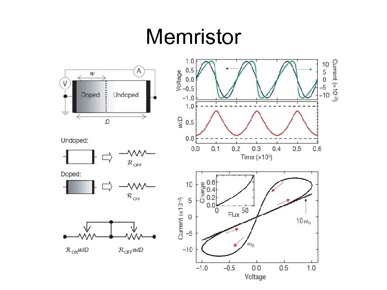 Memristor
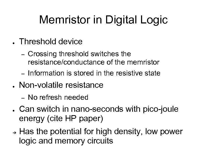 Memristor in Digital Logic ● Threshold device – – ● Crossing threshold switches the resistance/conductance of the memristor Information is stored in the resistive state Non-volatile resistance – ● ➔ No refresh needed Can switch in nano-seconds with pico-joule energy (cite HP paper) Has the potential for high density, low power logic and memory circuits
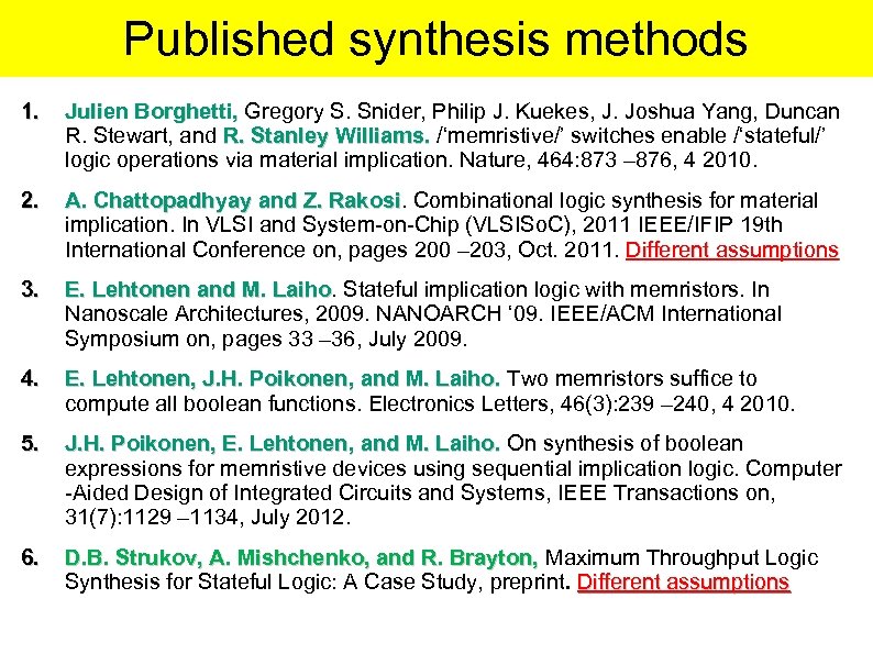 Published synthesis methods 1. Julien Borghetti, Gregory S. Snider, Philip J. Kuekes, J. Joshua Yang, Duncan R. Stewart, and R. Stanley Williams. /‘memristive/’ switches enable /‘stateful/’ logic operations via material implication. Nature, 464: 873 – 876, 4 2010. 2. A. Chattopadhyay and Z. Rakosi. Combinational logic synthesis for material Rakosi implication. In VLSI and System-on-Chip (VLSISo. C), 2011 IEEE/IFIP 19 th International Conference on, pages 200 – 203, Oct. 2011. Different assumptions 3. E. Lehtonen and M. Laiho. Stateful implication logic with memristors. In Laiho Nanoscale Architectures, 2009. NANOARCH ‘ 09. IEEE/ACM International Symposium on, pages 33 – 36, July 2009. 4. E. Lehtonen, J. H. Poikonen, and M. Laiho. Two memristors suffice to compute all boolean functions. Electronics Letters, 46(3): 239 – 240, 4 2010. 5. J. H. Poikonen, E. Lehtonen, and M. Laiho. On synthesis of boolean expressions for memristive devices using sequential implication logic. Computer -Aided Design of Integrated Circuits and Systems, IEEE Transactions on, 31(7): 1129 – 1134, July 2012. 6. D. B. Strukov, A. Mishchenko, and R. Brayton, Maximum Throughput Logic Synthesis for Stateful Logic: A Case Study, preprint. Different assumptions
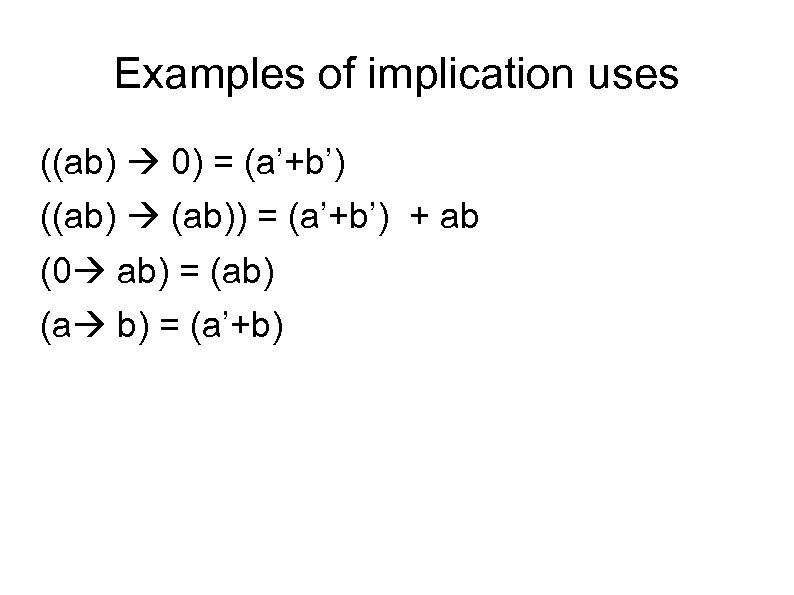
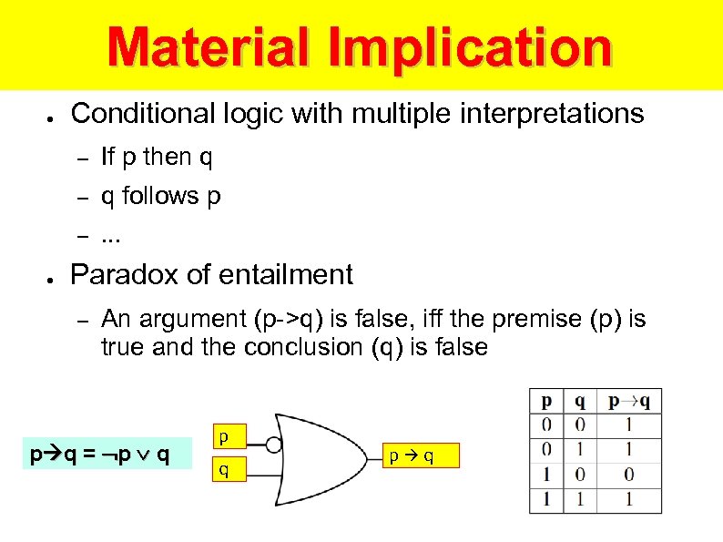 Material Implication ● Conditional logic with multiple interpretations – – q follows p – ● If p then q. . . Paradox of entailment – An argument (p->q) is false, iff the premise (p) is true and the conclusion (q) is false p q = p q p q
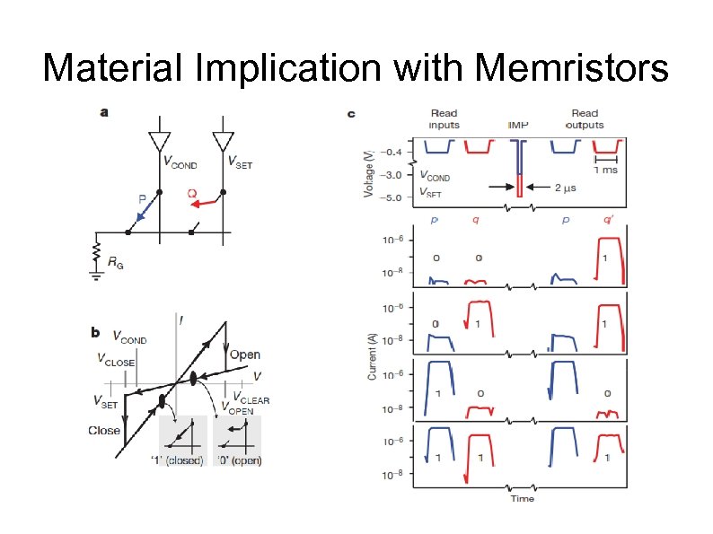
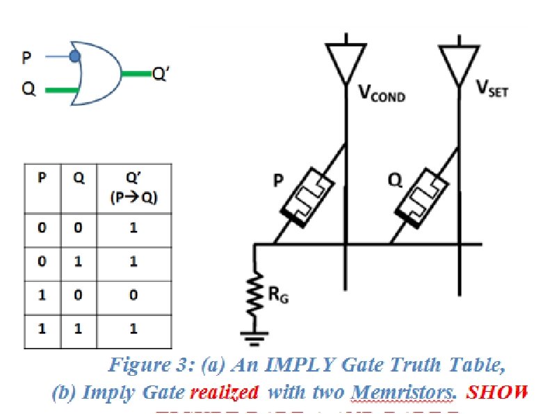
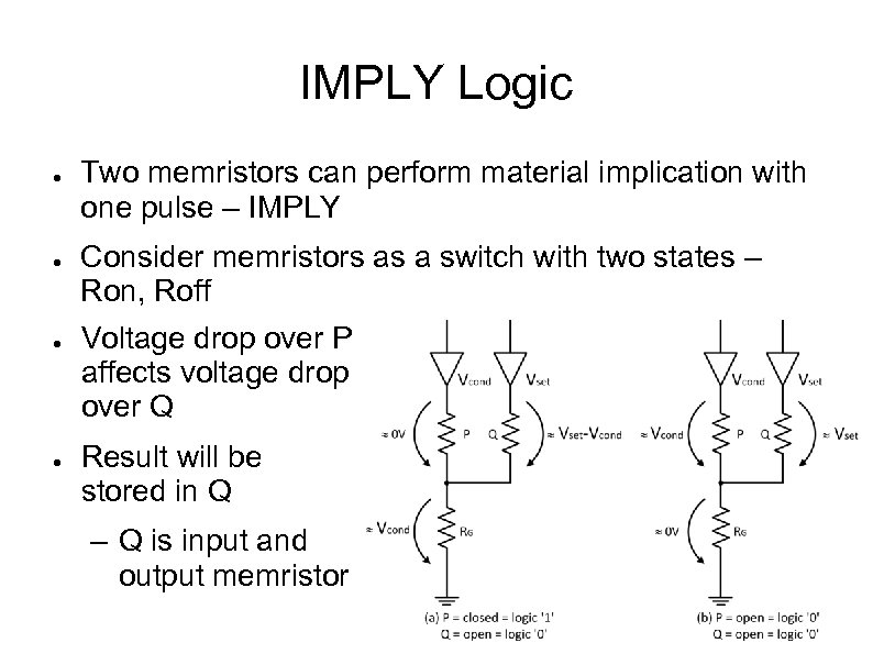 IMPLY Logic ● ● Two memristors can perform material implication with one pulse – IMPLY Consider memristors as a switch with two states – Ron, Roff Voltage drop over P affects voltage drop over Q Result will be stored in Q – Q is input and output memristor
 IMPLY Logic - Notes ● Explains the conditions for Q changing its state ● Q is pre-set to “ 0” (low conductance / high resistance) ● Voltage level V_Rg determines voltage drop over Q ● Only if P = “ 0” V_Rg remains low and allows Q to change
 Material Implication with Memristors
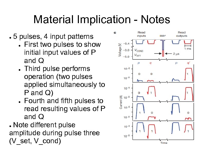 Material Implication - Notes 5 pulses, 4 input patterns ● First two pulses to show initial input values of P and Q ● Third pulse performs operation (two pulses applied simultaneously to P and Q) ● Fourth and fifth pulses to read resulting values of P and Q ● Note different pulse amplitude during pulse three (V_set, V_cond) ●
 Why are we interested in that? ● CMOS technology scaling is approaching limits ● Main limitation in modern CPUs is heat ● 2 -terminal device of 10 nm size – ● Allow much higher/denser device integration Switching between states can be done with pico Joule
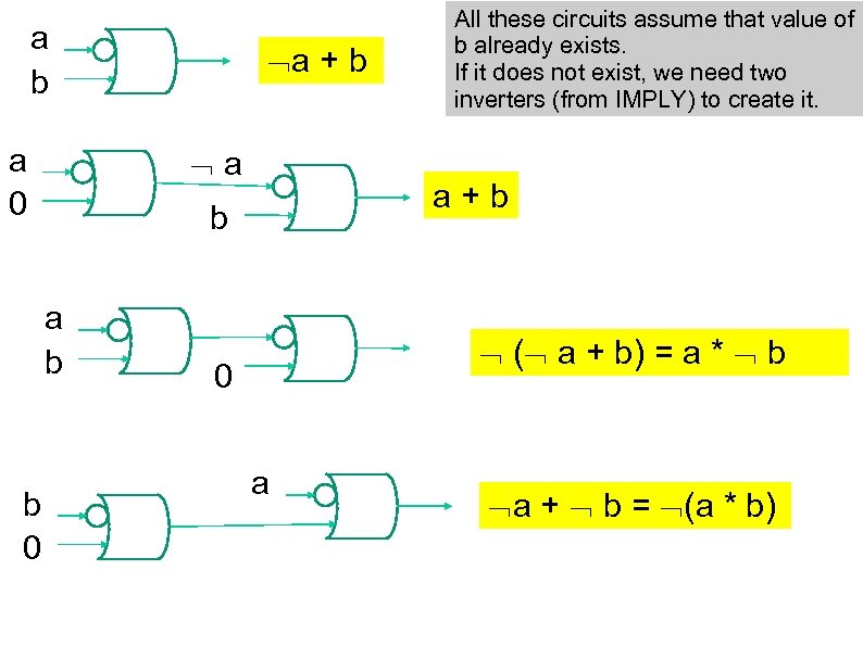
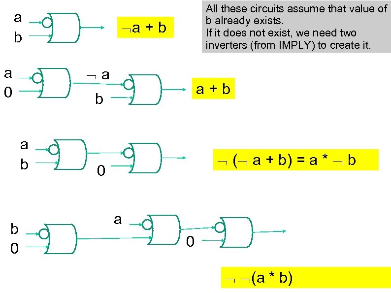
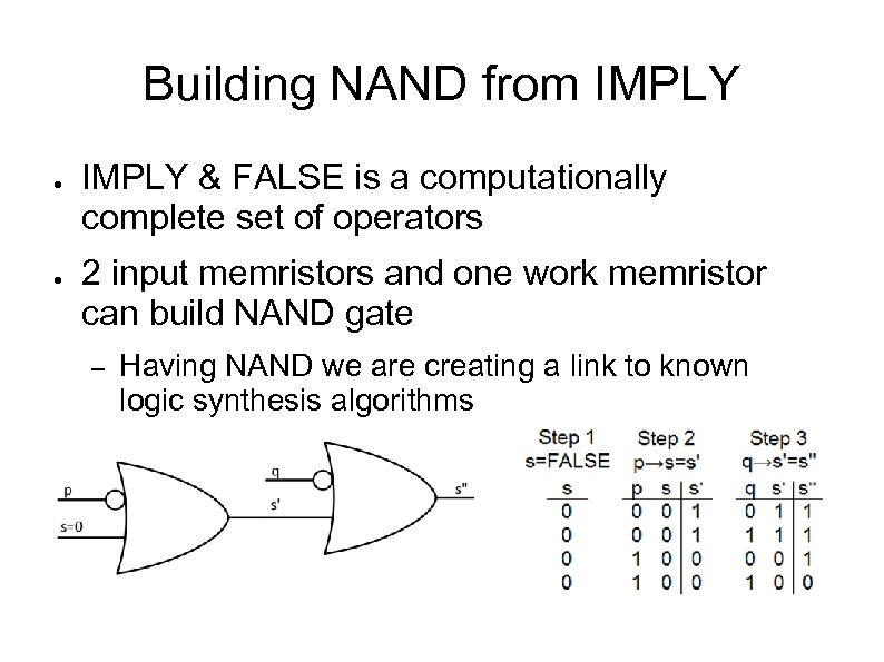 Building NAND from IMPLY ● ● IMPLY & FALSE is a computationally complete set of operators 2 input memristors and one work memristor can build NAND gate – Having NAND we are creating a link to known logic synthesis algorithms
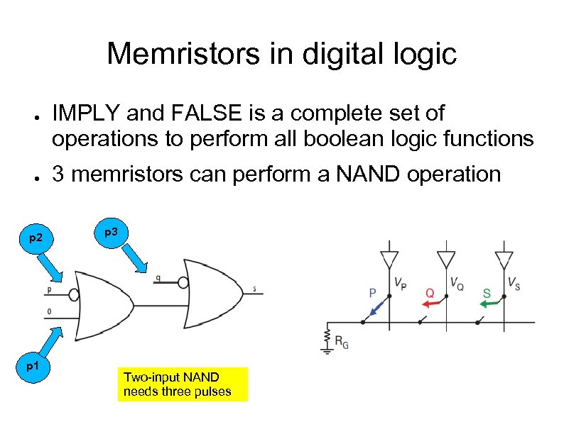 Memristors in digital logic ● ● p 2 p 1 IMPLY and FALSE is a complete set of operations to perform all boolean logic functions 3 memristors can perform a NAND operation p 3 Two-input NAND needs three pulses
 Examples of implication uses ((ab) 0) = (a’+b’) ((ab) (ab)) = (a’+b’) + ab (0 ab) = (ab) (a b) = (a’+b)
 a b a a 0 a+b b a b b 0 a + b All these circuits assume that value of b already exists. If it does not exist, we need two inverters (from IMPLY) to create it. ( a + b) = a * b 0 a a + b = (a * b)
 a b a + b a a 0 a+b b a b b 0 All these circuits assume that value of b already exists. If it does not exist, we need two inverters (from IMPLY) to create it. ( a + b) = a * b 0 a 0 (a * b)
 Now we assume that all inputs must be created with Stateful IMPLY technology from scratch.
 NOT & OR
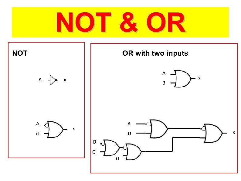 NOT & OR NOT OR with two inputs A A 0 A x B x A x 0 B 0 x
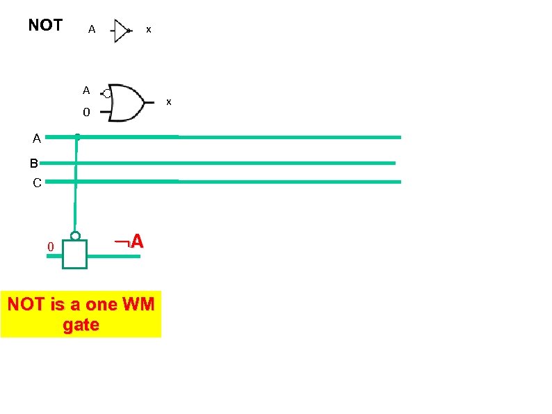 NOT A x 0 A B C 0 A NOT is a one WM gate
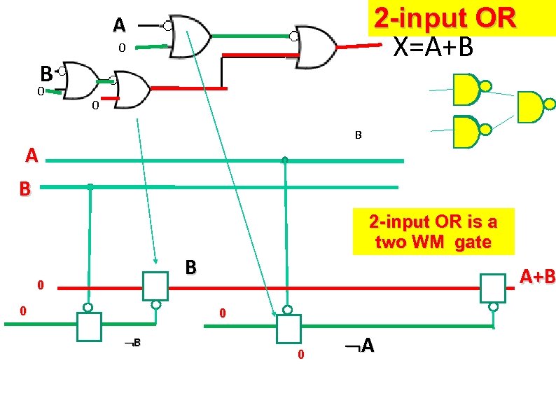 2 -input OR A X=A+B 0 B 0 B A B 2 -input OR is a two WM gate B 0 0 A+B 0 A
 NAND & AND
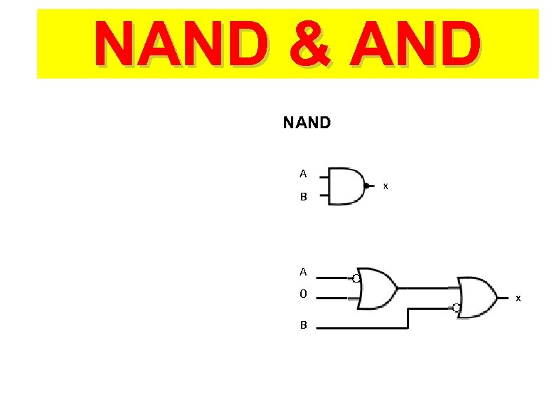 NAND && AND NAND A B x A 0 B x
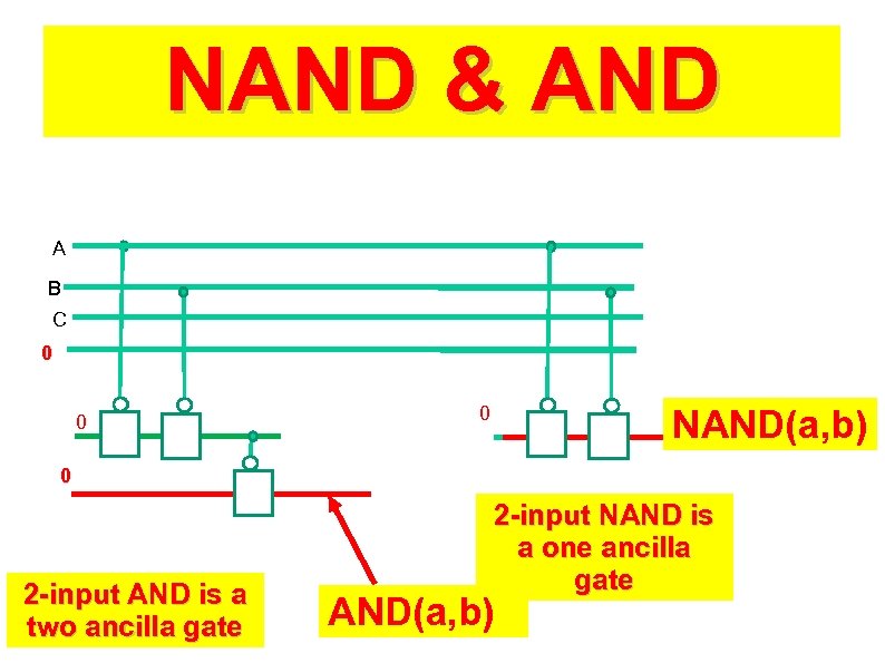 NAND & AND A B C 0 0 0 NAND(a, b) 0 2 -input AND is a two ancilla gate 2 -input NAND is a one ancilla gate AND(a, b)
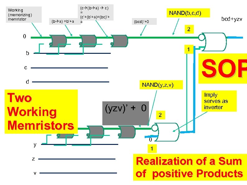 Working (memorizing) memristor (b a) =b’+a (c (b a) c) = (c’+(b’+a)=(bc)’+ a NAND(b, c, d) (bcd)’+0 bcd+yzv 2 0 1 b c d NAND(y, z, v) Two Working 0 Memristors y z v SOP Imply serves as inverter (yzv)’ + 0 2 0 1 Realization of a Sum of positive Products
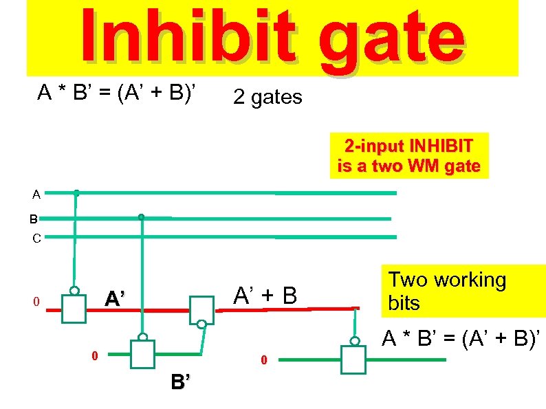 Inhibit gate A * B’ = (A’ + B)’ 2 gates 2 -input INHIBIT is a two WM gate A B C A’ + B A’ 0 Two working bits A * B’ = (A’ + B)’ 0 0 B’
 NOR Gates
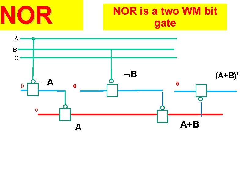 NOR is a two WM bit gate A B C A 0 B 0 (A+B)’ 0 0 A A+B
 EXOR Gates
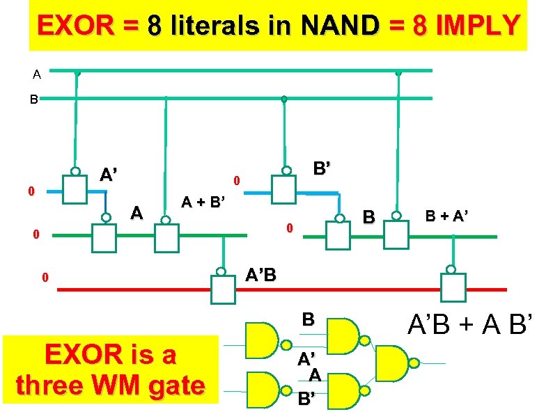 EXOR = 8 literals in NAND = 8 IMPLY A B A’ 0 B’ 0 A A + B’ 0 0 0 B A’B B EXOR is a three WM gate B + A’ A’ A B’ A’B + A B’
 SYNTHESIS WITH EXORS WITH NO LIMIT ON NUMBER OF ANCILLA BITS
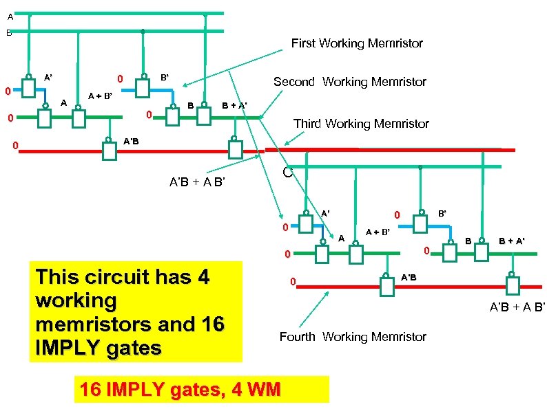 A B First Working Memristor 0 A’ 0 A B’ A + B’ 0 0 0 Second Working Memristor B B + A’ Third Working Memristor A’B + A B’ C 0 A’ 0 A B’ A + B’ 0 0 This circuit has 4 working memristors and 16 IMPLY gates 0 B B + A’ A’B + A B’ Fourth Working Memristor 16 IMPLY gates, 4 WM
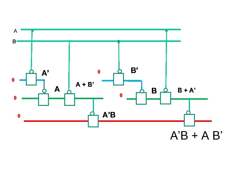 A B A’ 0 B’ 0 A A + B’ 0 0 0 B B + A’ A’B + A B’
 MUX
MUX
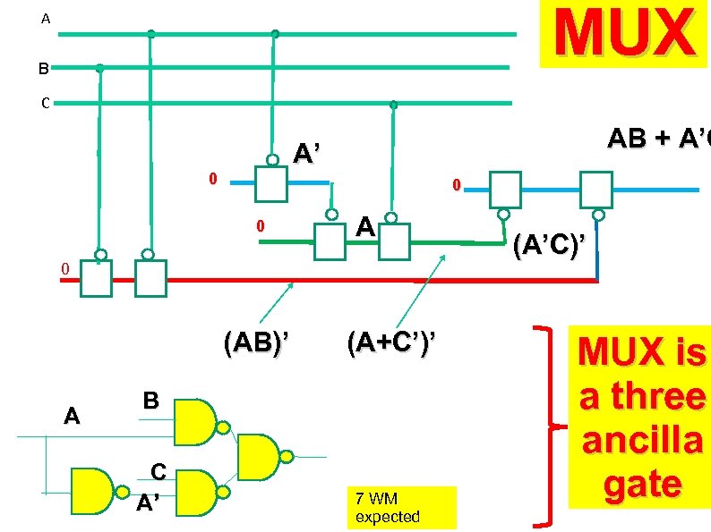 MUX A B C AB + A’C A’ 0 0 0 A 0 (AB)’ A (A+C’)’ B C A’ 7 WM expected (A’C)’ MUX is a three ancilla gate
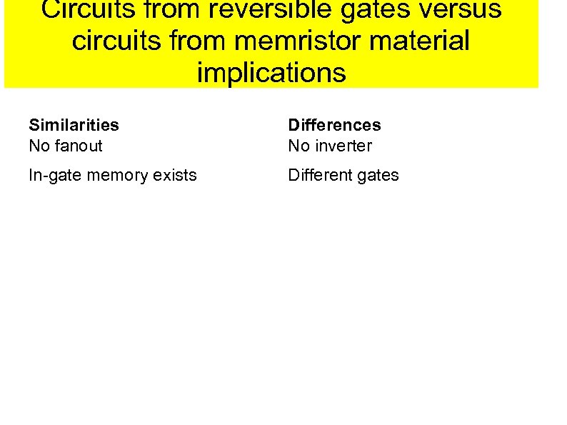 Circuits from reversible gates versus circuits from memristor material implications Similarities No fanout Differences No inverter In-gate memory exists Different gates
 Examples of typical multiinput gates
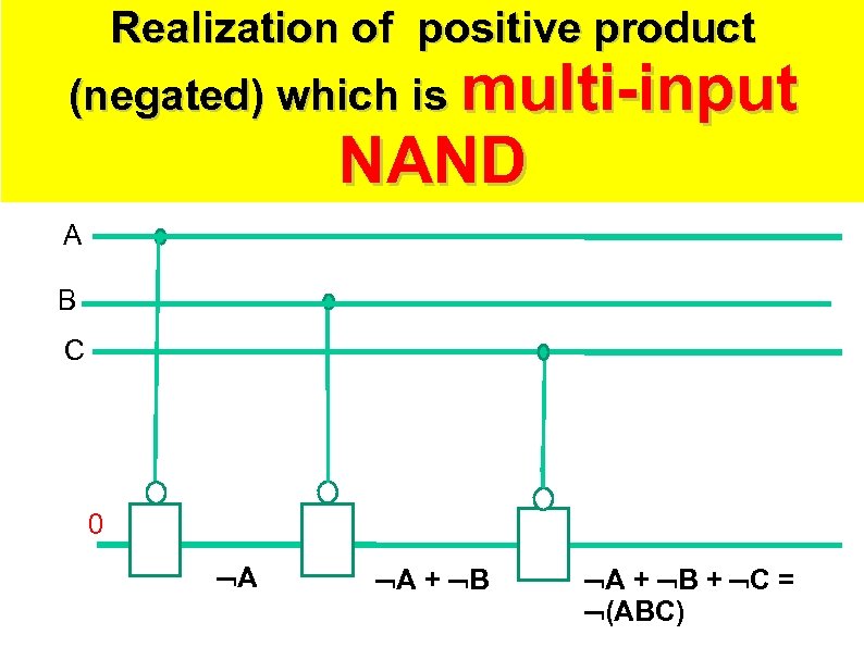 Realization of positive product (negated) which is multi-input NAND A B C 0 A A + B + C = (ABC)
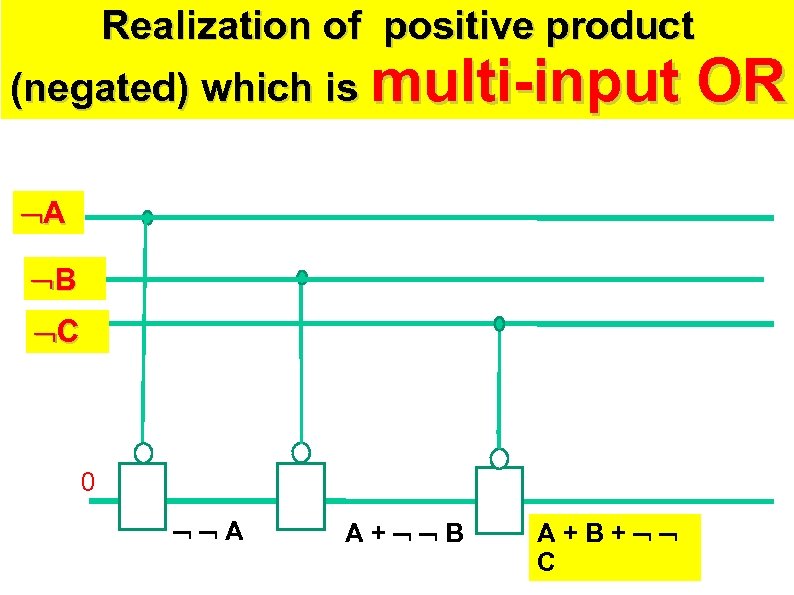 Realization of positive product (negated) which is multi-input A B C 0 A A+ B A+B+ C OR
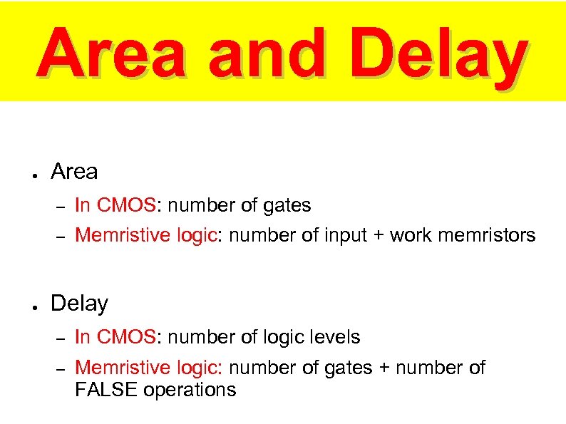 Area and Delay ● Area – – ● In CMOS: number of gates Memristive logic: number of input + work memristors Delay – In CMOS: number of logic levels – Memristive logic: number of gates + number of FALSE operations
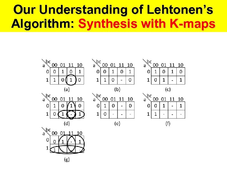 Our Understanding of Lehtonen’s Algorithm: Synthesis with K-maps
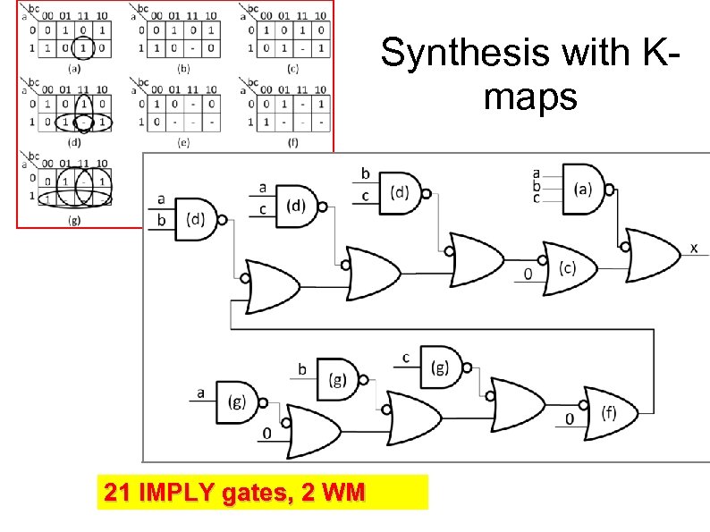 Synthesis with Kmaps 21 IMPLY gates, 2 WM
 Variants of synthesis algorithms 1. Find all groups in every level (Lehtonen). 1. Find only groups corresponding to essential primes and secondary essential primes. 1. Find minimum SOP cover of F and SOP cover of F’ and use groups that correspond to primes from these covers. 1. Use cost heuristics related to best prime selection.
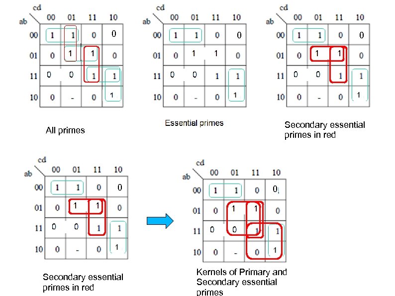 0 0 0 Secondary essential primes in red All primes 0 Secondary essential primes in red 0 Kernels of Primary and Secondary essential primes
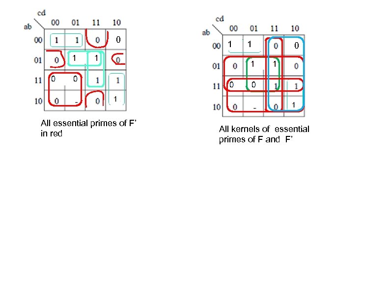 0 All essential primes of F’ in red 1 1 0 All kernels of essential primes of F and F’
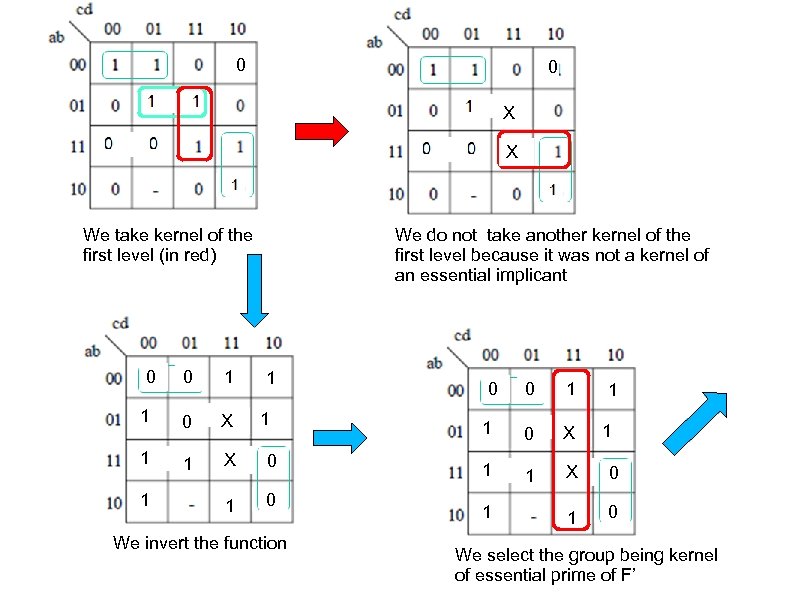 0 0 X X We take kernel of the first level (in red) 0 We do not take another kernel of the first level because it was not a kernel of an essential implicant 0 1 1 0 X 1 1 X 0 1 1 We invert the function 0 0 1 1 0 X 1 1 X 0 1 1 We select the group being kernel of essential prime of F’
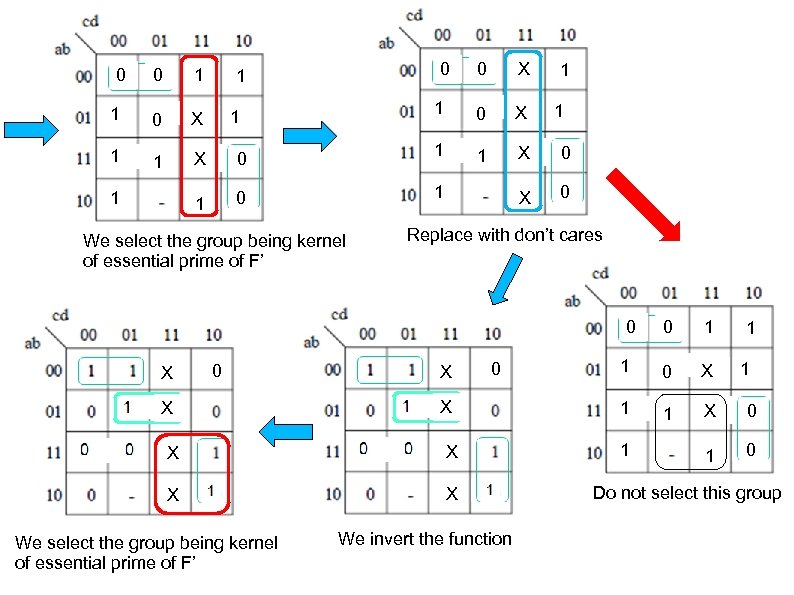 0 0 1 1 0 X 1 1 X 1 0 1 X 0 X 1 0 1 0 1 0 1 X 0 1 We select the group being kernel of essential prime of F’ 1 Replace with don’t cares 0 X X X We select the group being kernel of essential prime of F’ We invert the function 0 1 1 0 X 1 1 X 0 1 1 Do not select this group
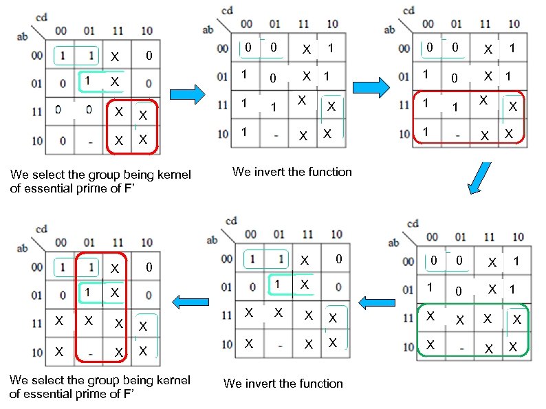 X X X We select the group being kernel of essential prime of F’ X 0 X 1 0 0 0 X 1 1 1 X X 0 X X X We select the group being kernel of essential prime of F’ X 1 1 X 0 1 1 0 X X 1 X X X 0 X 1 X X 0 1 0 X X 1 1 0 X We invert the function X X X 0 1 0 0 X X X X We invert the function X X 1 0 1 1 0 X X
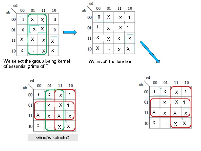 X X X X 1 X X X X X We select the group being kernel of essential prime of F’ 0 X X 1 X X X 0 0 X X 1 0 1 1 0 X X Groups selected X X 1 0 1 1 0 X X We invert the function 0 X X 1 X X X X 1 0 1 1 0 X X
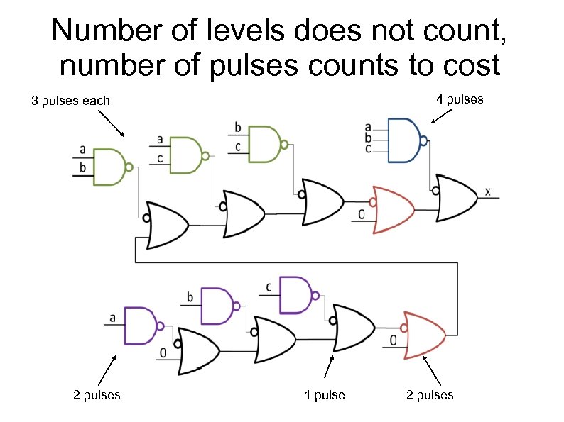 Number of levels does not count, number of pulses counts to cost 4 pulses 3 pulses each 2 pulses 1 pulse 2 pulses
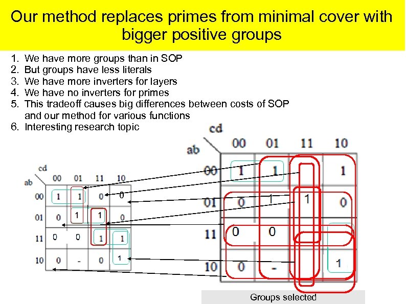 Our method replaces primes from minimal cover with bigger positive groups 1. 2. 3. 4. 5. We have more groups than in SOP But groups have less literals We have more inverters for layers We have no inverters for primes This tradeoff causes big differences between costs of SOP and our method for various functions 6. Interesting research topic 0 0 1 Groups selected
 ABC and Automated Logic Synthesis 1. 1. Can we use existing tools to perform synthesis? How do we integrate memristor logic to these tools? Are the results valid with respect to memristor logic specifics (area, delay)?
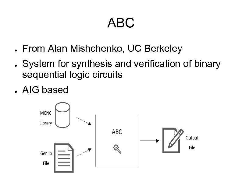 ABC ● ● ● From Alan Mishchenko, UC Berkeley System for synthesis and verification of binary sequential logic circuits AIG based
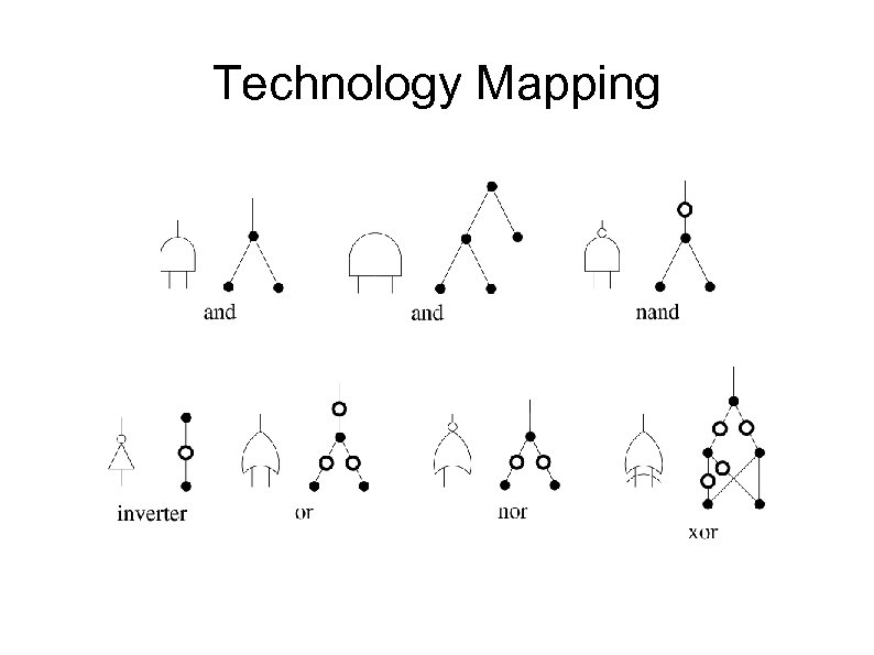 Technology Mapping
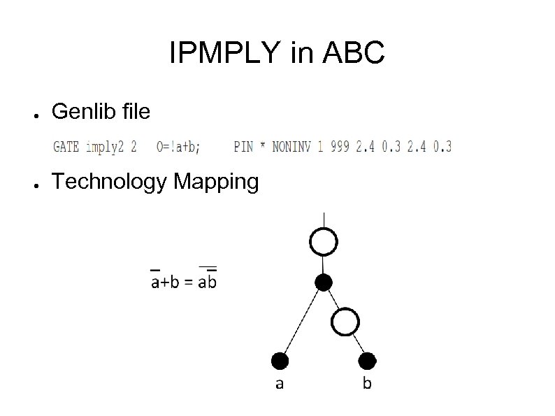 IPMPLY in ABC ● Genlib file ● Technology Mapping
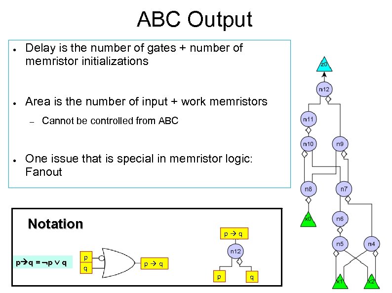 ABC Output ● ● Delay is the number of gates + number of memristor initializations Area is the number of input + work memristors – ● Cannot be controlled from ABC One issue that is special in memristor logic: Fanout Notation p q = p q p q p q
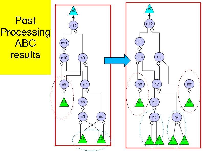
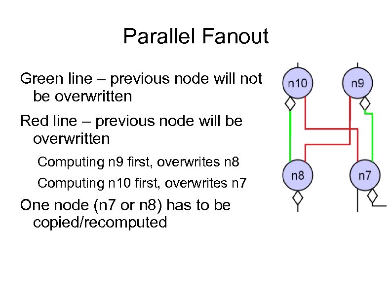 Parallel Fanout Green line – previous node will not be overwritten Red line – previous node will be overwritten Computing n 9 first, overwrites n 8 Computing n 10 first, overwrites n 7 One node (n 7 or n 8) has to be copied/recomputed
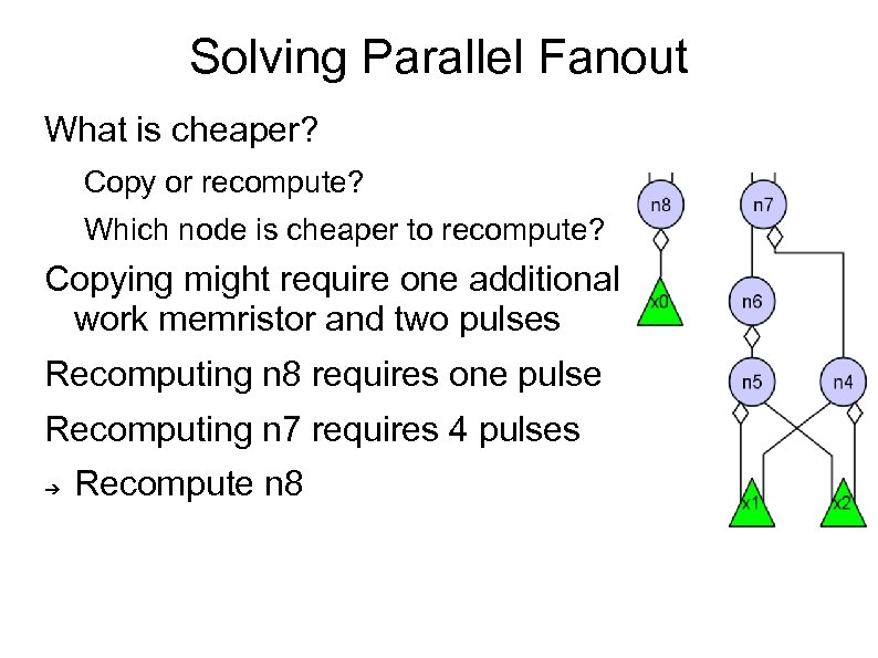 Solving Parallel Fanout What is cheaper? Copy or recompute? Which node is cheaper to recompute? Copying might require one additional work memristor and two pulses Recomputing n 8 requires one pulse Recomputing n 7 requires 4 pulses ➔ Recompute n 8
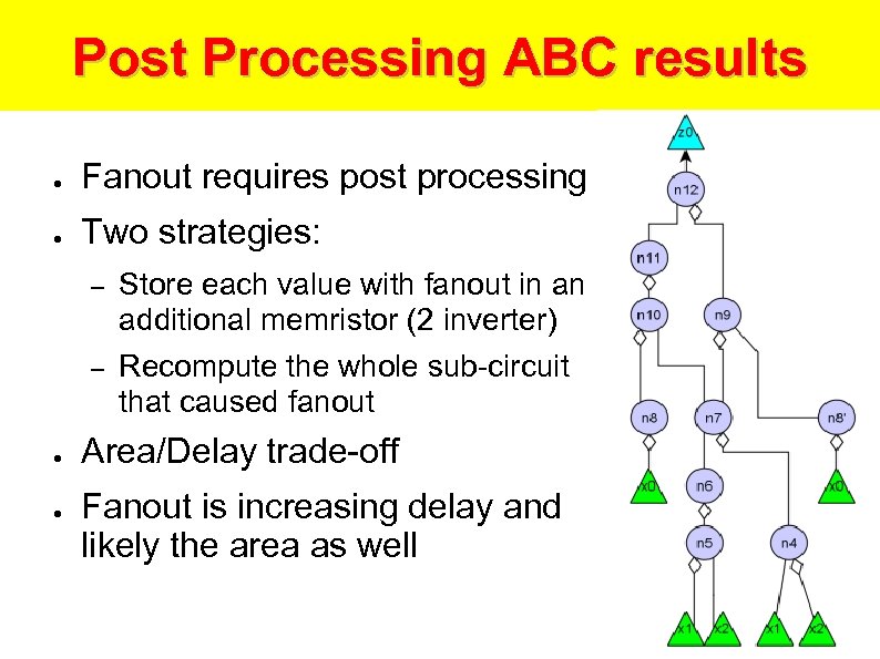 Post Processing ABC results ● Fanout requires post processing ● Two strategies: – – ● ● Store each value with fanout in an additional memristor (2 inverter) Recompute the whole sub-circuit that caused fanout Area/Delay trade-off Fanout is increasing delay and likely the area as well
 Post Processing ABC results
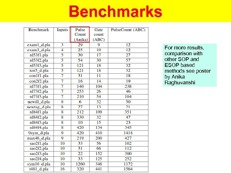 Benchmarks For more results, comparison with other SOP and ESOP based methods see poster by Anika Raghuvanshi
 Benchmarks - Notes Pulse Count (Anika) ● Solution for minimum number of work memristors (minimum area) ● Follows similar approach as presented with the kmaps ● Pulse count = delay ● Gate count ● Number of IMPLY gates as computed by ABC ● Can contain fan-out that has to be post-processed ● Is not area optimized (more than 2 work memristors) ● Pulse Count (ABC) ● Post processed to avoid harmful fan-out ● Still not area optimized ●
 Conclusions 1. Very little published on synthesis with IMPLY gates 1. Very little published on synthesis with memristors. 1. Although logic synthesis for memristors may seem similar to standard SOP or multi-level combinational synthesis, it is different because of assumption of minimal level number of Working Memristors? 2. We created methods to synthesize circuits with minimum number of working memristors 3. We created methods to synthesize circuits with small but not minimal (3, 4) working memristors. 1. Research question: “how important is this assumption for future memristor technologies? ”
 Future works 1. Synthesize for given fixed number of working memristors 2. Compare various synthesis methods: 1. SOP 2. ESOP 3. TANT 4. NAND Tree 5. Bi-decomposition 6. Ashenhurst-Curtis decomposition 3. Analyze tradeoffs between various methods for various types of functions (symmetric, unate, linear, self-dual, etc).
 Future works 1. Synthesis of pipelined, systolic circuits 2. Synthesis of Finite State Machines and sequential circuits built from blocks. 3. Fuzzy and multiple-valued circuits. 4. Exact synthesis

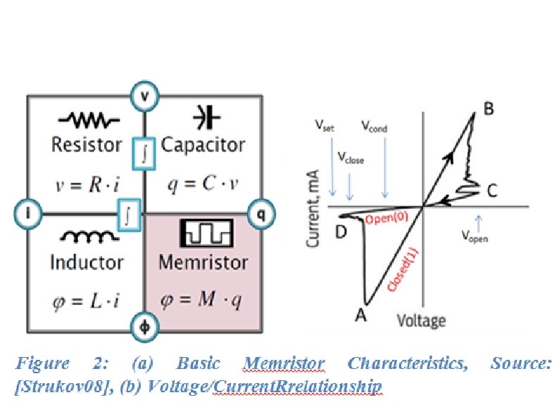
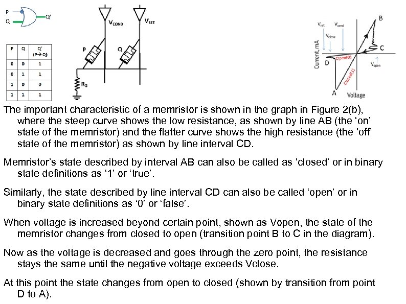 The important characteristic of a memristor is shown in the graph in Figure 2(b), where the steep curve shows the low resistance, as shown by line AB (the ‘on’ state of the memristor) and the flatter curve shows the high resistance (the ‘off’ state of the memristor) as shown by line interval CD. Memristor’s state described by interval AB can also be called as ‘closed’ or in binary state definitions as ‘ 1’ or ‘true’. Similarly, the state described by line interval CD can also be called ‘open’ or in binary state definitions as ‘ 0’ or ‘false’. When voltage is increased beyond certain point, shown as Vopen, the state of the memristor changes from closed to open (transition point B to C in the diagram). Now as the voltage is decreased and goes through the zero point, the resistance stays the same until the negative voltage exceeds Vclose. At this point the state changes from open to closed (shown by transition from point D to A).
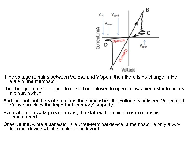 If the voltage remains between VClose and VOpen, then there is no change in the state of the memristor. The change from state open to closed and closed to open, allows memristor to act as a binary switch. And the fact that the state remains the same when the voltage is between Vopen and Vclose provides the important ‘memory’ property. Even when the voltage is removed, the state will remain the same, and is remembered. Observe that while a transistor is a three-terminal device, a memristor is only a twoterminal device which simplifies the layout.
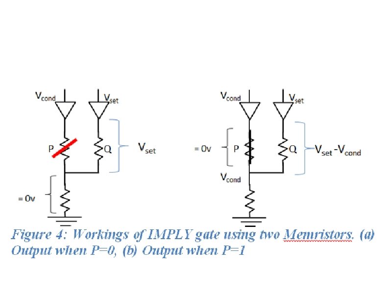
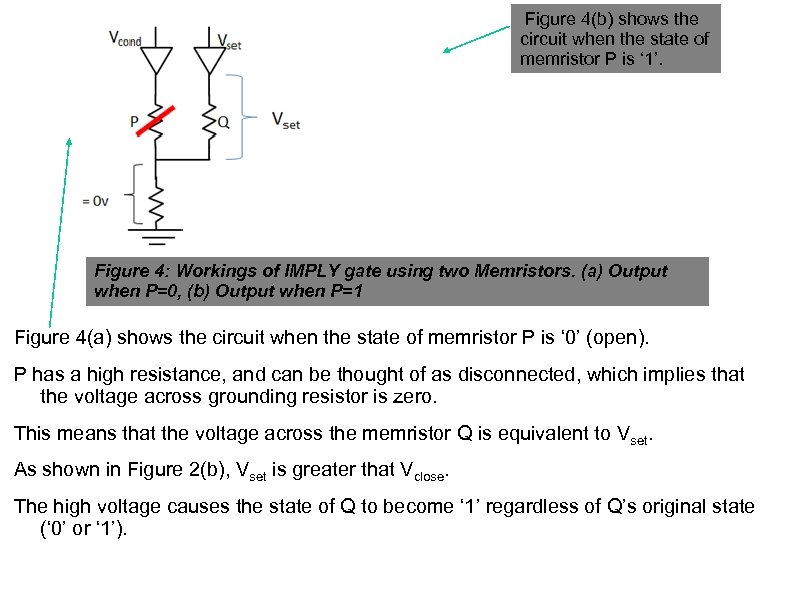 Figure 4(b) shows the circuit when the state of memristor P is ‘ 1’. Figure 4: Workings of IMPLY gate using two Memristors. (a) Output when P=0, (b) Output when P=1 Figure 4(a) shows the circuit when the state of memristor P is ‘ 0’ (open). P has a high resistance, and can be thought of as disconnected, which implies that the voltage across grounding resistor is zero. This means that the voltage across the memristor Q is equivalent to Vset. As shown in Figure 2(b), Vset is greater that Vclose. The high voltage causes the state of Q to become ‘ 1’ regardless of Q’s original state (‘ 0’ or ‘ 1’).
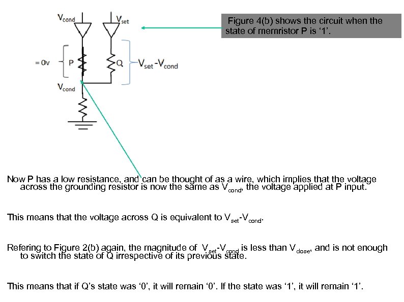 Figure 4(b) shows the circuit when the state of memristor P is ‘ 1’. Now P has a low resistance, and can be thought of as a wire, which implies that the voltage across the grounding resistor is now the same as Vcond, the voltage applied at P input. This means that the voltage across Q is equivalent to Vset-Vcond. Refering to Figure 2(b) again, the magnitude of Vset-Vcond is less than Vclose, and is not enough to switch the state of Q irrespective of its previous state. This means that if Q’s state was ‘ 0’, it will remain ‘ 0’. If the state was ‘ 1’, it will remain ‘ 1’.
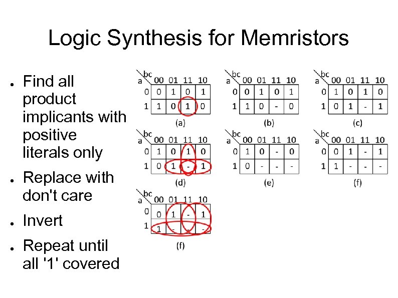 Logic Synthesis for Memristors ● ● Find all product implicants with positive literals only Replace with don't care Invert Repeat until all '1' covered
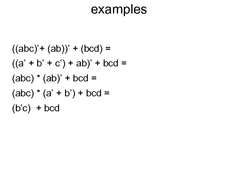 examples ((abc)’+ (ab))’ + (bcd) = ((a’ + b’ + c’) + ab)’ + bcd = (abc) * (a’ + b’) + bcd = (b’c) + bcd
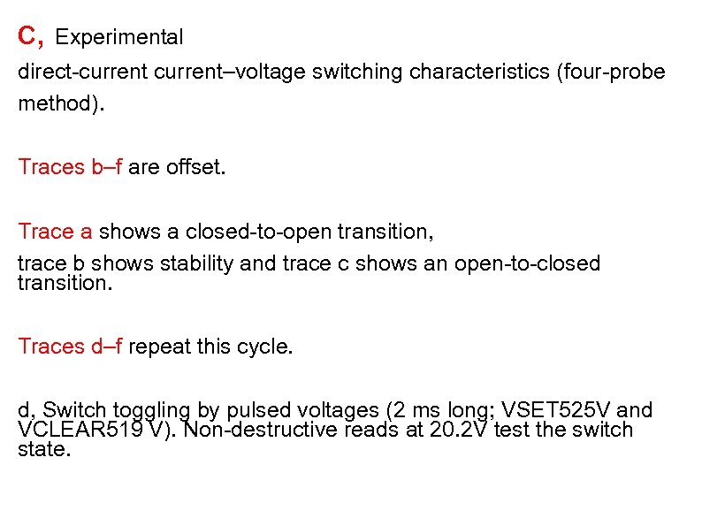 c, Experimental direct-current–voltage switching characteristics (four-probe method). Traces b–f are offset. Trace a shows a closed-to-open transition, trace b shows stability and trace c shows an open-to-closed transition. Traces d–f repeat this cycle. d, Switch toggling by pulsed voltages (2 ms long; VSET 525 V and VCLEAR 519 V). Non-destructive reads at 20. 2 V test the switch state.
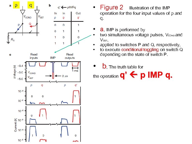 p q • Figure 2 Illustration of the IMP operation for the four input values of p and q. • a, IMP is performed by • • • two simultaneous voltage pulses, VCOND and VSET, applied to switches P and Q, respectively, to execute conditional toggling on switch Q depending on the state of switch P. • b, The truth table for the operation q’ p IMP q.
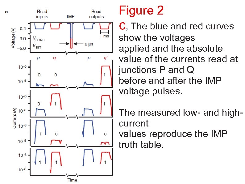 Figure 2 c, The blue and red curves show the voltages applied and the absolute value of the currents read at junctions P and Q before and after the IMP voltage pulses. The measured low- and highcurrent values reproduce the IMP truth table.


