7526fd3eb606acf2819f770f0ddecf9f.ppt
- Количество слайдов: 40
 Digital Integrated Circuits A Design Perspective Jan M. Rabaey Anantha Chandrakasan Borivoje Nikolic Modified and integrated by Davide Bertozzi Design Methodologies Array-based design © Digital Integrated Circuits 2 nd Design Methodologie
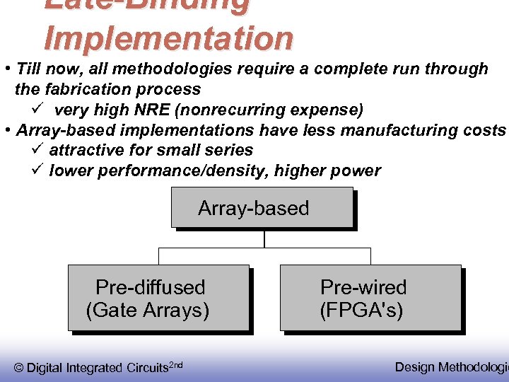 Late-Binding Implementation • Till now, all methodologies require a complete run through the fabrication process ü very high NRE (nonrecurring expense) • Array-based implementations have less manufacturing costs ü attractive for small series ü lower performance/density, higher power Array-based Pre-diffused (Gate Arrays) © Digital Integrated Circuits 2 nd Pre-wired (FPGA's) Design Methodologie
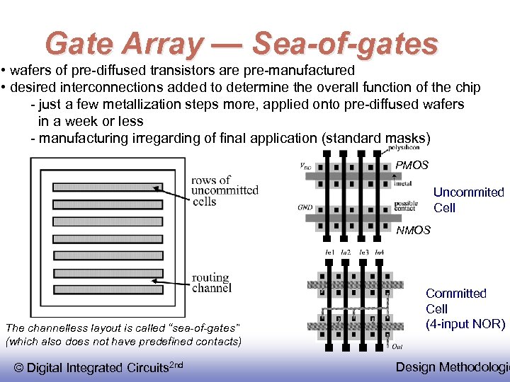 Gate Array — Sea-of-gates • wafers of pre-diffused transistors are pre-manufactured • desired interconnections added to determine the overall function of the chip - just a few metallization steps more, applied onto pre-diffused wafers in a week or less - manufacturing irregarding of final application (standard masks) PMOS Uncommited Cell NMOS The channelless layout is called “sea-of-gates” (which also does not have predefined contacts) © Digital Integrated Circuits 2 nd Committed Cell (4 -input NOR) Design Methodologie
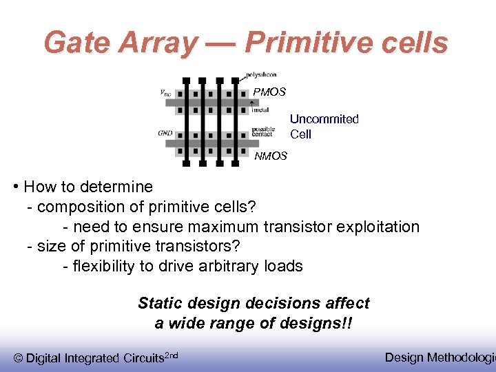 Gate Array — Primitive cells PMOS Uncommited Cell NMOS • How to determine - composition of primitive cells? - need to ensure maximum transistor exploitation - size of primitive transistors? - flexibility to drive arbitrary loads Static design decisions affect a wide range of designs!! © Digital Integrated Circuits 2 nd Design Methodologie
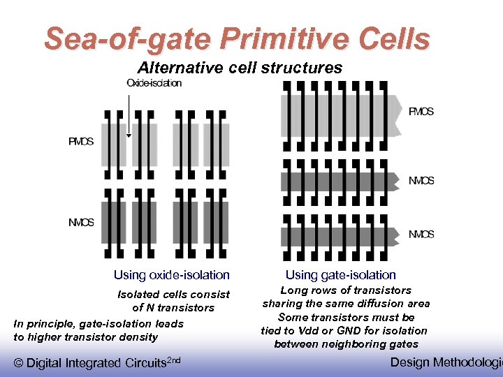 Sea-of-gate Primitive Cells Alternative cell structures Using oxide-isolation Isolated cells consist of N transistors In principle, gate-isolation leads to higher transistor density © Digital Integrated Circuits 2 nd Using gate-isolation Long rows of transistors sharing the same diffusion area Some transistors must be tied to Vdd or GND for isolation between neighboring gates Design Methodologie
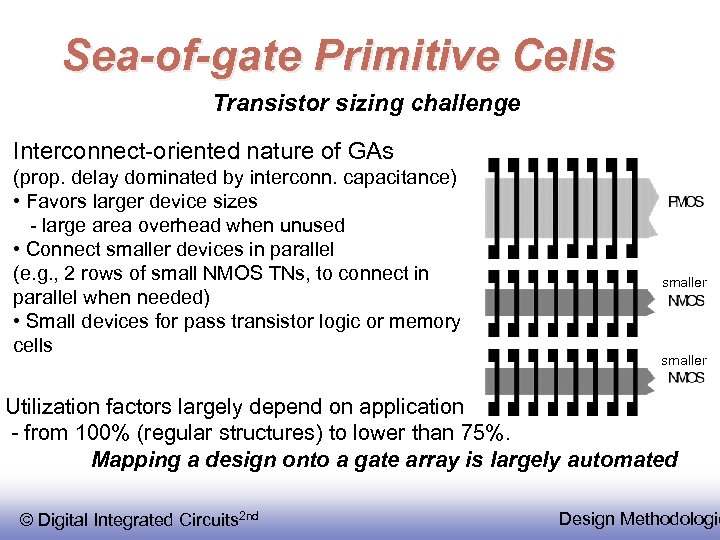 Sea-of-gate Primitive Cells Transistor sizing challenge Interconnect-oriented nature of GAs (prop. delay dominated by interconn. capacitance) • Favors larger device sizes - large area overhead when unused • Connect smaller devices in parallel (e. g. , 2 rows of small NMOS TNs, to connect in parallel when needed) • Small devices for pass transistor logic or memory cells smaller Utilization factors largely depend on application Using oxide-isolation - from 100% (regular structures) to lower than 75%. Mapping a design onto a gate array is largely automated © Digital Integrated Circuits 2 nd Design Methodologie
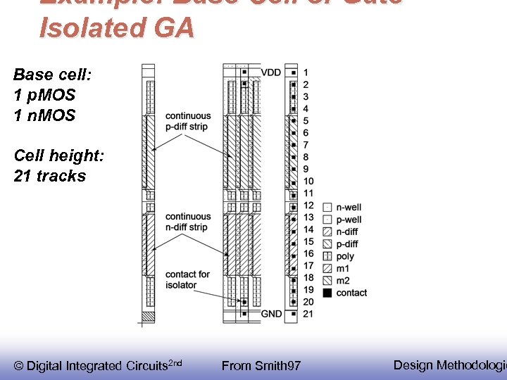 Example: Base Cell of Gate. Isolated GA Base cell: 1 p. MOS 1 n. MOS Cell height: 21 tracks © Digital Integrated Circuits 2 nd From Smith 97 Design Methodologie
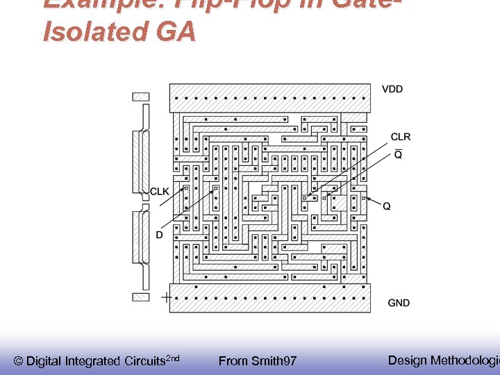 Example: Flip-Flop in Gate. Isolated GA © Digital Integrated Circuits 2 nd From Smith 97 Design Methodologie
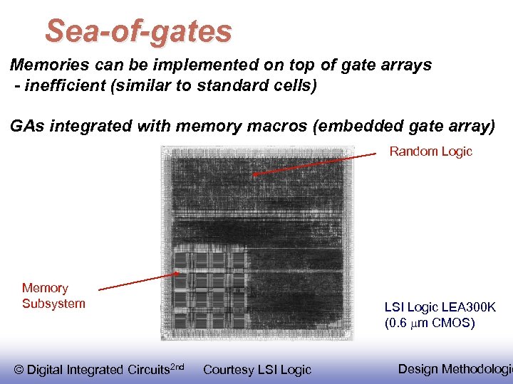 Sea-of-gates Memories can be implemented on top of gate arrays - inefficient (similar to standard cells) GAs integrated with memory macros (embedded gate array) Random Logic Memory Subsystem © Digital Integrated Circuits 2 nd LSI Logic LEA 300 K (0. 6 mm CMOS) Courtesy LSI Logic Design Methodologie
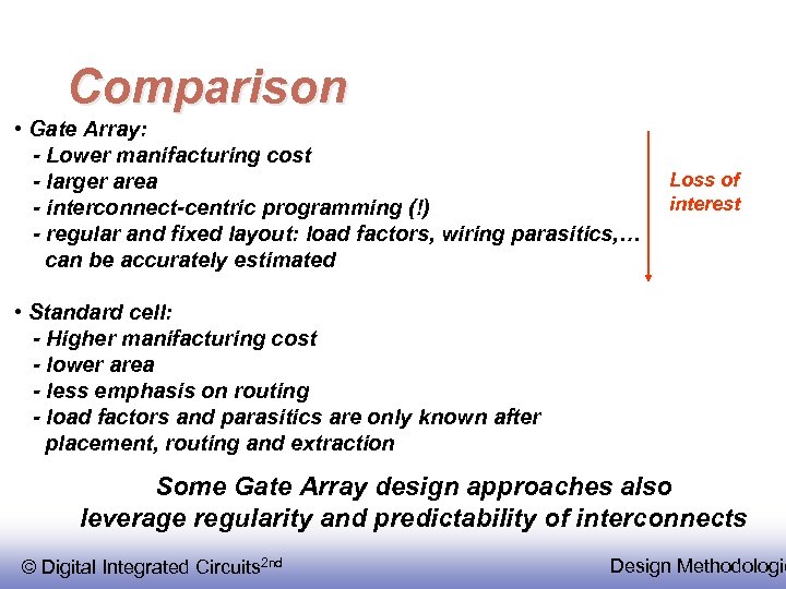 Comparison • Gate Array: - Lower manifacturing cost - larger area - interconnect-centric programming (!) - regular and fixed layout: load factors, wiring parasitics, … can be accurately estimated Loss of interest • Standard cell: - Higher manifacturing cost - lower area - less emphasis on routing - load factors and parasitics are only known after placement, routing and extraction Some Gate Array design approaches also leverage regularity and predictability of interconnects © Digital Integrated Circuits 2 nd Design Methodologie
 The return of gate arrays? Array of prediffused cells with a superimposed wiring grid Via programmable gate array (VPGA) Via-programmable cross-point metal-5 metal-6 programmable via Exploits regularity of interconnects © Digital Integrated Circuits 2 nd [Pileggi 02] Design Methodologie
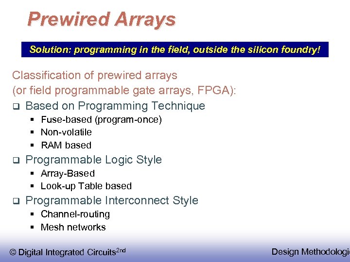 Prewired Arrays Solution: programming in the field, outside the silicon foundry! Classification of prewired arrays (or field programmable gate arrays, FPGA): q Based on Programming Technique § Fuse-based (program-once) § Non-volatile § RAM based q Programmable Logic Style § Array-Based § Look-up Table based q Programmable Interconnect Style § Channel-routing § Mesh networks © Digital Integrated Circuits 2 nd Design Methodologie
 Prewired Arrays Starting from a regular array of cells…. . q How do we implement programmable logic? How can we commit logic to perform any possible boolean function? q How do we store the program/configuration that commits the programmable array to a certain logic function? © Digital Integrated Circuits 2 nd Design Methodologie
 Configuration storage q q q Fuse-based FPGA - Use of fuses (to be blown) or antifuses (to be short-circuited) - small area overhead vs one-time-programmable Nonvolative FPGA - program stored in EEPROM/Flash - functionality retained until next programming round - Additional process steps (e. g. , ultrathin oxides), high programming voltages Volatile FPGA - program stored in RAM cells - at power up, configuration re-loading from external non-volatile memory - RAM cells programmed as a giant shift register - linear programming vs multi-cell programming - regular CMOS process is OK - logic function can be dynamically modified on the fly during execution (partial reconfiguration capability) © Digital Integrated Circuits 2 nd Design Methodologie
 Antifuse-Based FPGA antifuse polysilicon 10 nm ONO dielectric n+ antifuse diffusion Open by default, closed by applying current pulse (melting of the dielectric) The opposite holds for FUSES © Digital Integrated Circuits 2 nd From Smith 97 Design Methodologie
 Prewired Arrays …. starting from a regular array of cells…. . q How do we implement programmable logic? How can we commit logic to perform any possible boolean function? § Array-based approach § Cell-based approach q How do we store the program/configuration that dedicates the programmable array to a certain logic function? © Digital Integrated Circuits 2 nd Design Methodologie
 Logic (programmable logic devices, PLD) Include input in the minterm Include minterm in the output I 5 I 4 I 3 I 2 I 1 I 0 Programmable OR array I 3 Programmable AND array I 1 I 0 Programmable OR array Fixed AND array O 3 O 2 O 1 O 0 PLA I 2 I 5 I 4 I 3 I 2 I 1 I 0 Fixed OR array Programmable AND array O 3 O 2 O 1 O 0 Fixed, trade-off flexibility for density and power PROM O 3 O 2 O 1 O 0 PAL Indicates programmable connection © Digital Integrated Circuits 2 nd Indicates fixed connection Design Methodologie
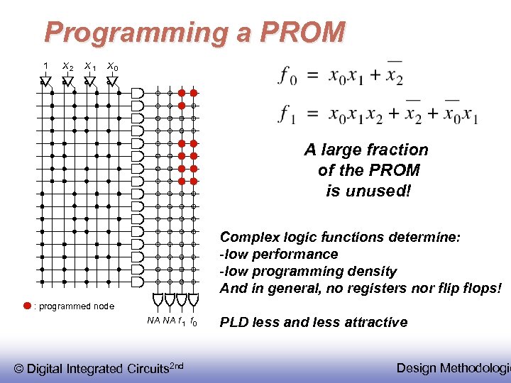 Programming a PROM 1 X 2 X 1 X 0 A large fraction of the PROM is unused! Complex logic functions determine: -low performance -low programming density And in general, no registers nor flip flops! : programmed node NA NA f 1 f 0 © Digital Integrated Circuits 2 nd PLD less and less attractive Design Methodologie
 More Complex PAL How can I implement sequential logic with PLDs? x Outputs can be fed back as a subset of the inputs Programmable D, T, J-K or clocked S-R flip flop i inputs, j minterms/macrocell, k macrocells © Digital Integrated Circuits 2 nd From Smith 97 Design Methodologie
 Multi-level logic advantages Reduced sum of products form: x=ADF + AEF + BDF + BEF + CDF + CEF + G A D F A E F B D F B E F C D F C E F G 1 6 x 3 -input AND gates + 1 x 7 -input OR gate (may not exist!) 25 wires (19 literals plus 6 internal wires) 2 A B C 3 4 5 7 x 1 D E 2 3 4 x F G Factored form: 6 x = (A + B + C) (D + E) F + G 1 x 3 -input OR gate, 2 x 2 -input OR gates, 1 x 3 -input AND gate 10 wires (7 literals plus 3 internal wires) Such optimizations 2 nd unsopported by PLAs © Digital Integrated Circuits are Design Methodologie
 Array-based Programmable Logic q + REGULAR STRUCTURE § accurate parasitic, area, power, speed estimates q + SUITABLE FOR 2 -LEVEL LOGIC § E. g. functions with a large fan-in §. . or functions that map well into 2 -level logic (e. g. , FSMs) q - HIGHER OVERHEAD § capacitance of intermediate nodes § negatively affects performance and power § risk of underutilization, especially PLAs (and waste of power) The alternative is CELL-BASED PROGRAMMABLE LOGIC…. © Digital Integrated Circuits 2 nd Design Methodologie
 2 -input mux as programmable logic block A mux used as logic function generator Configuration A A 0 F B 1 S B S F= 0 0 X Y Y 1 1 1 0 X Y Y 0 0 1 0 1 1 X Y X X X Y 1 0 X Y XY X+ Y X Y 1 By properly connecting inputs A, B and S to variables X and Y, 10 different logic functions can be obtained © Digital Integrated Circuits 2 nd Design Methodologie
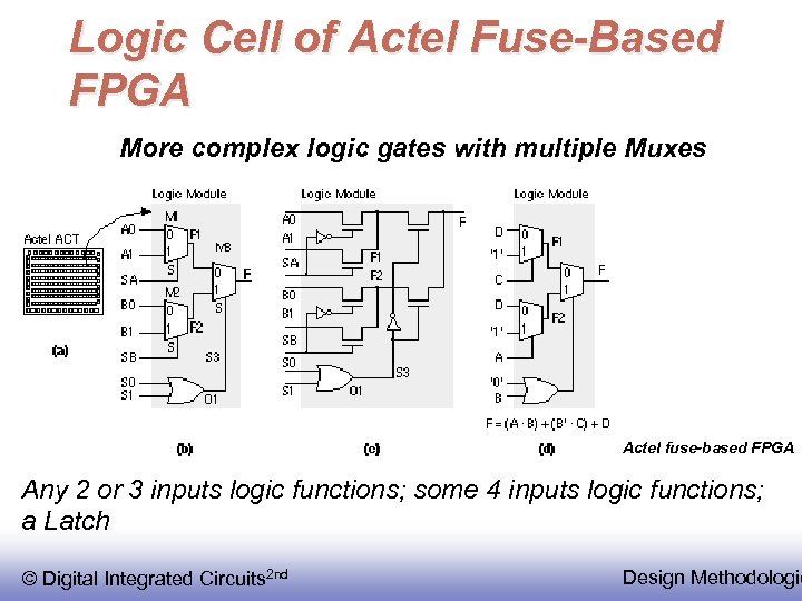 Logic Cell of Actel Fuse-Based FPGA More complex logic gates with multiple Muxes Used in Actel fuse-based FPGA Any 2 or 3 inputs logic functions; some 4 inputs logic functions; a Latch © Digital Integrated Circuits 2 nd Design Methodologie
 Look-up Table Based Logic Cell EXOR inference The Look-up table stores the truth table of a logic function (with n inputs, any logic function of n inputs can be implemented) © Digital Integrated Circuits 2 nd Design Methodologie
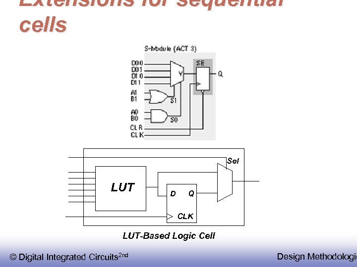 Extensions for sequential cells Sel LUT D Q CLK LUT-Based Logic Cell © Digital Integrated Circuits 2 nd Design Methodologie
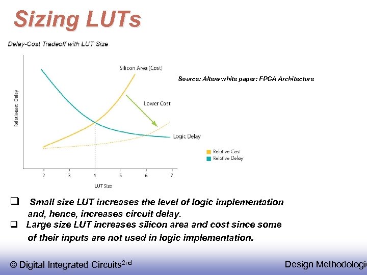 Sizing LUTs Source: Altera white paper: FPGA Architecture q Small size LUT increases the level of logic implementation and, hence, increases circuit delay. q Large size LUT increases silicon area and cost since some of their inputs are not used in logic implementation. © Digital Integrated Circuits 2 nd Design Methodologie
 LUT-Based Logic Cell Complex cells by adding more LUTs, increasing LUT size and inserting flip-flops and Muxes 4 C 1. . C 4 xx D 4 D 3 D 2 Logic function of xxx D 1 F 3 F 2 F 1 Logic function of xxx x xxxxx CLB for Xilinx 4000 Series © Digital Integrated Circuits 2 nd xxxx Bits control xx xx Logic function x of xxx F 4 xxxx xx x x Bits control xx xx xxxx xx xx H P x x Multiplexer Controlled by Configuration Program Courtesy Xilinx Design Methodologie
 q How to make interconnects programmable? © Digital Integrated Circuits 2 nd Design Methodologie
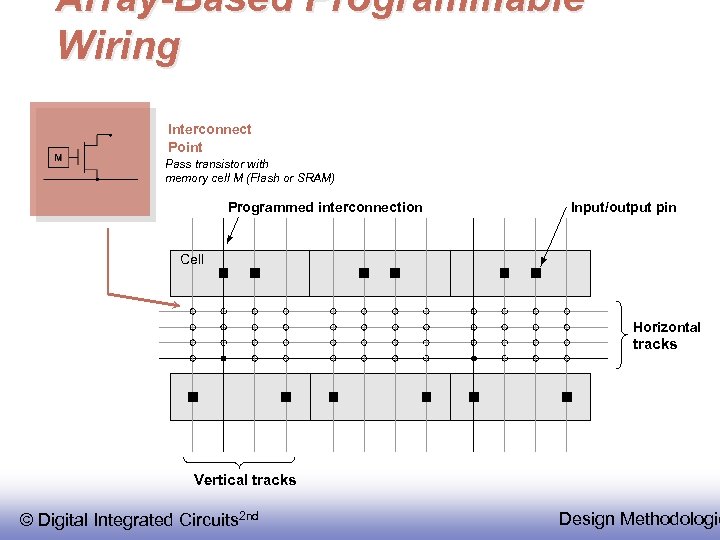 Array-Based Programmable Wiring Interconnect Point Pass transistor with memory cell M (Flash or SRAM) Programmed interconnection Input/output pin Cell Horizontal tracks Vertical tracks © Digital Integrated Circuits 2 nd Design Methodologie
 Crossing points q q Pass transistor large number of transistors and control signals High fan-out wires delay and power Fuse/antifuse Fuses: long programming times (few connections usually needed) Antifuses require less programming one time programmable Array-based wire programming has been successful only in the write-once class of FPGAs © Digital Integrated Circuits 2 nd Design Methodologie
 Network Each logic cell output routed north, west, south or east Connectivity through RAM-programmable switching or connect matrices Switch Box Connect Box Interconnect Point © Digital Integrated Circuits 2 nd Courtesy Dehon and Wawrzyniek Design Methodologie
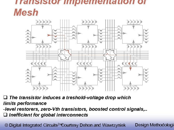 Transistor Implementation of Mesh q The transistor induces a treshold-voltage drop which limits performance -level restorers, zero-Vth transistors, boosted control signals, . . q Inefficient for global interconnects © Digital Integrated Circuits 2 nd Courtesy Dehon and Wawrzyniek Design Methodologie
 Hierarchical Mesh Network • Most mesh-based FPGA architectures offer alternative wiring resources allowing for effective global wiring • Reduced fanout and reduced resistance © Digital Integrated Circuits 2 nd Courtesy Dehon and Wawrzyniek Design Methodologie
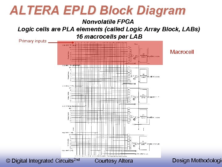 ALTERA EPLD Block Diagram Nonvolatile FPGA Logic cells are PLA elements (called Logic Array Block, LABs) 16 macrocells per LAB Primary inputs Macrocell © Digital Integrated Circuits 2 nd Courtesy Altera Design Methodologie
 Altera MAX © Digital Integrated Circuits 2 nd From Smith 97 Design Methodologie
 Altera MAX Interconnect Architecture column channel row channel t PIA LAB 1 LAB 2 LAB PIA t PIA LAB 6 Array-based (MAX 3000 -7000) Simple, predictable does not scale well © Digital Integrated Circuits 2 nd Mesh-based (MAX 9000) Wide channels (48 to 96 wires) Beyond 560 macrocells Courtesy Altera Design Methodologie
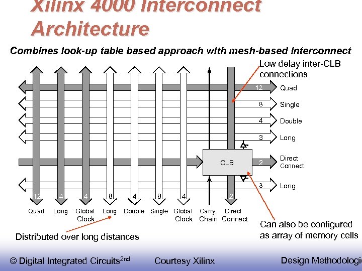 Xilinx 4000 Interconnect Architecture Combines look-up table based approach with mesh-based interconnect Low delay inter-CLB connections 12 8 Single 4 Double 3 CLB Quad Long 2 3 12 4 4 8 Quad Long Global Long 4 8 4 Double Single Global Clock Connect Long 2 Carry Direct Clock Chain Connect Distributed over long distances © Digital Integrated Circuits 2 nd Direct Courtesy Xilinx Can also be configured as array of memory cells Design Methodologie
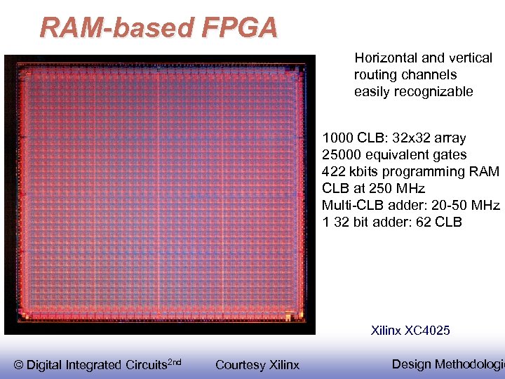 RAM-based FPGA Horizontal and vertical routing channels easily recognizable 1000 CLB: 32 x 32 array 25000 equivalent gates 422 kbits programming RAM CLB at 250 MHz Multi-CLB adder: 20 -50 MHz 1 32 bit adder: 62 CLB Xilinx XC 4025 © Digital Integrated Circuits 2 nd Courtesy Xilinx Design Methodologie
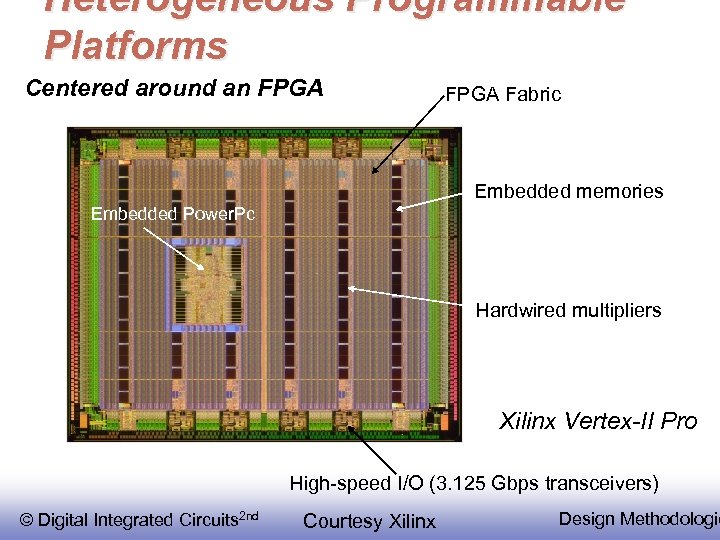 Heterogeneous Programmable Platforms Centered around an FPGA Fabric Embedded memories Embedded Power. Pc Hardwired multipliers Xilinx Vertex-II Pro High-speed I/O (3. 125 Gbps transceivers) © Digital Integrated Circuits 2 nd Courtesy Xilinx Design Methodologie
 Berkeley Pleiades Processor Centered around an ARM 7 core FPGA Reconfigurable Data-path Interface ARM 8 Core © Digital Integrated Circuits 2 nd - ARM 8: system manager - Intensive computations offloaded to a reconfigurable datapath (adders, multipliers, ASIP, . . ) - FPGA for bit manipulation • 0. 25 um 6 -level metal CMOS • 5. 2 mm x 6. 7 mm • 1. 2 Million transistors • 40 MHz at 1 V • 2 extra supplies: 0. 4 V, 1. 5 V • 1. 5~2 m. W power dissipation Design Methodologie


