85481f814e1a536b821a8bc3852114ae.ppt
- Количество слайдов: 41
Digital Design: Combinational Logic Blocks Credits: Slides adapted from: J. F. Wakerly, Digital Design, 4/e, Prentice Hall, 2006 C. H. Roth, Fundamentals of Logic Design 5/e, Thomson, 2004 , A. B. Marcovitz, Intro. to Logic and Computer Design Mc. Graw Hill, 2008 , R. H. Katz, G. Borriello, Contemporary Logic Design 2/e, Prentice-Hall, 2005 , 1
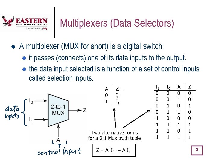
Multiplexers (Data Selectors) l A multiplexer (MUX for short) is a digital switch: it passes (connects) one of its data inputs to the output. l the data input selected is a function of a set of control inputs called selection inputs. l A 0 1 Z I 0 I 1 Two alternative forms for a 2: 1 Mux truth table Z = A' I 0 + A I 1 0 0 1 1 I 0 0 0 1 1 A 0 1 0 1 Z 0 0 1 1 1 2
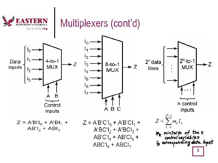
Multiplexers (cont’d) 3
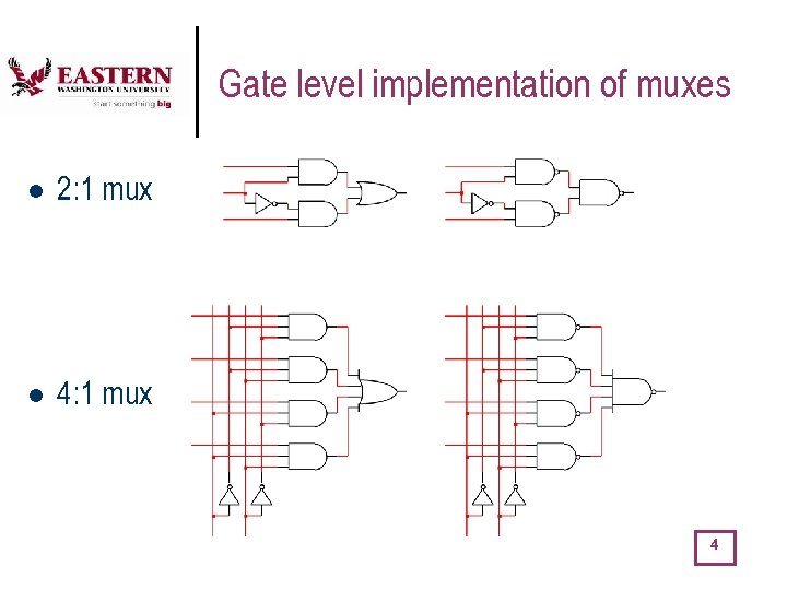
Gate level implementation of muxes l 2: 1 mux l 4: 1 mux 4
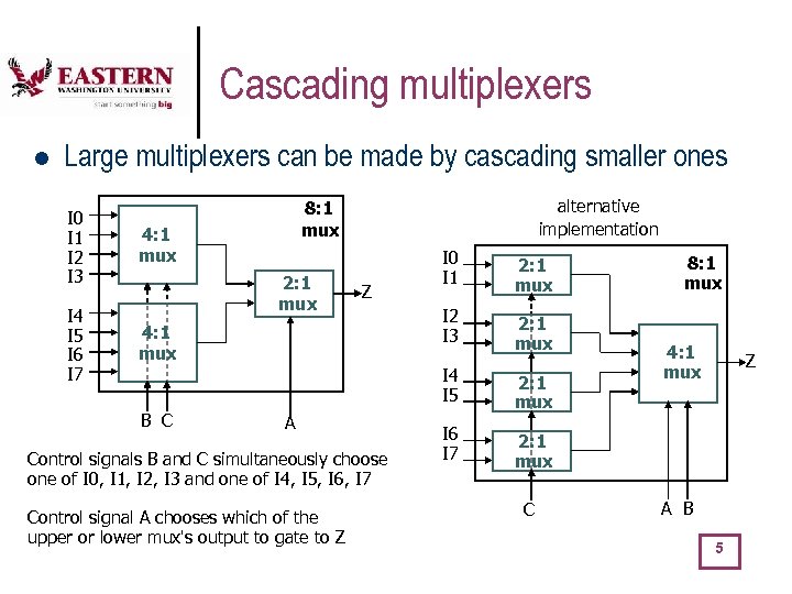
Cascading multiplexers l Large multiplexers can be made by cascading smaller ones I 0 I 1 I 2 I 3 4: 1 mux I 4 I 5 I 6 I 7 alternative implementation 8: 1 mux 4: 1 mux 2: 1 mux Z I 0 I 1 2: 1 mux I 2 I 3 2: 1 mux I 4 I 5 B C A Control signals B and C simultaneously choose one of I 0, I 1, I 2, I 3 and one of I 4, I 5, I 6, I 7 Control signal A chooses which of the upper or lower mux's output to gate to Z 2: 1 mux I 6 I 7 8: 1 mux 4: 1 mux Z 2: 1 mux C A B 5
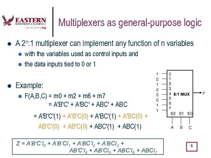
Multiplexers as general-purpose logic l A 2 n: 1 multiplexer can implement any function of n variables l l l with the variables used as control inputs and the data inputs tied to 0 or 1 Example: l F(A, B, C) = m 0 + m 2 + m 6 + m 7 = A'B'C' + A'BC' + ABC = A'B'C'(1) + A'B'C(0) + A'BC'(1) + A'BC(0) + AB'C'(0) + AB'C(0) + ABC'(1) + ABC(1) 1 0 0 0 1 1 Z = A'B'C'I 0 + A'B'CI 1 + A'BC'I 2 + A'BCI 3 + AB'C'I 4 + AB'CI 5 + ABC'I 6 + ABCI 7 0 1 2 3 4 8: 1 MUX 5 6 7 S 2 S 1 S 0 A B C 6 Z F
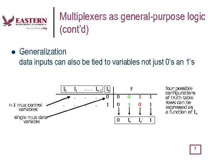
Multiplexers as general-purpose logic (cont’d) l Generalization data inputs can also be tied to variables not just 0’s an 1’s I 0 single mux data variable . . . In-1 In . n-1 mux control variables I 1 F . . . 0 0 0 1 1 . . 1 0 1 0 In In' four possible configurations of truth table rows can be expressed as a function of In 1 7
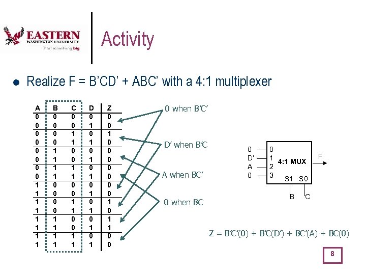
Activity l Realize F = B’CD’ + ABC’ with a 4: 1 multiplexer A 0 0 0 0 1 1 1 1 B 0 0 0 0 1 1 1 1 C 0 0 1 1 D 0 1 0 1 Z 0 0 1 0 0 0 0 1 1 0 0 0 when B’C’ D’ when B’C A when BC’ 0 when BC 0 D’ A 0 0 1 4: 1 MUX 2 3 S 1 S 0 B F C Z = B’C’(0) + B’C(D’) + BC’(A) + BC(0) 8
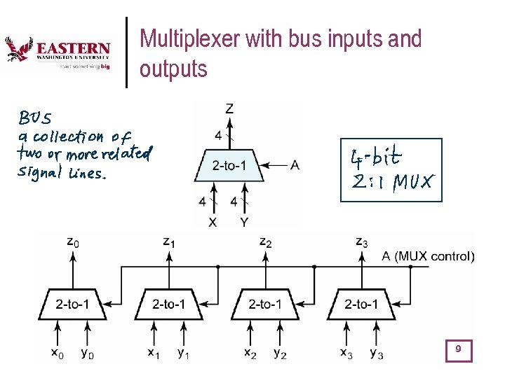
Multiplexer with bus inputs and outputs 9
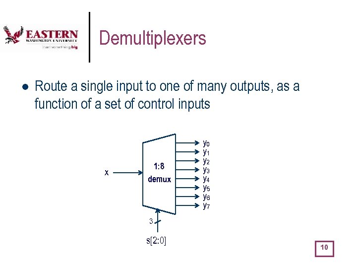
Demultiplexers l Route a single input to one of many outputs, as a function of a set of control inputs x 1: 8 demux y 0 y 1 y 2 y 3 y 4 y 5 y 6 y 7 3 s[2: 0] 10
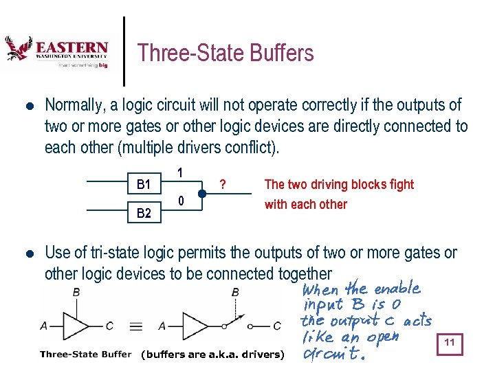
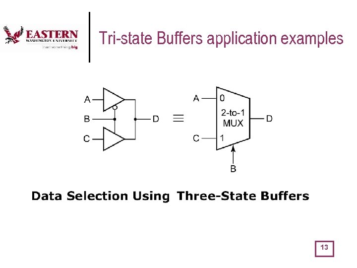
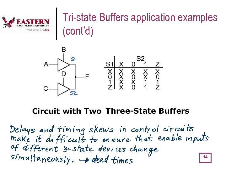
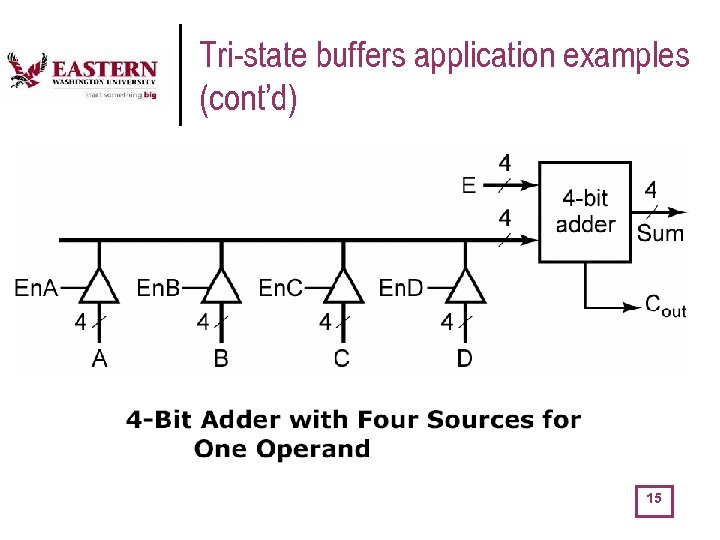
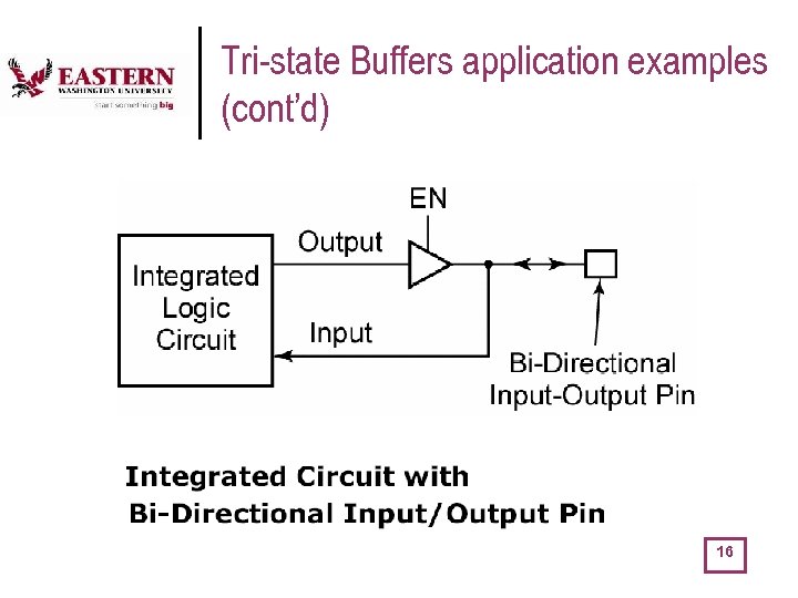
Three-State Buffers l Normally, a logic circuit will not operate correctly if the outputs of two or more gates or other logic devices are directly connected to each other (multiple drivers conflict). B 1 B 2 l 1 0 ? The two driving blocks fight with each other Use of tri-state logic permits the outputs of two or more gates or other logic devices to be connected together 11 (buffers are a. k. a. drivers)
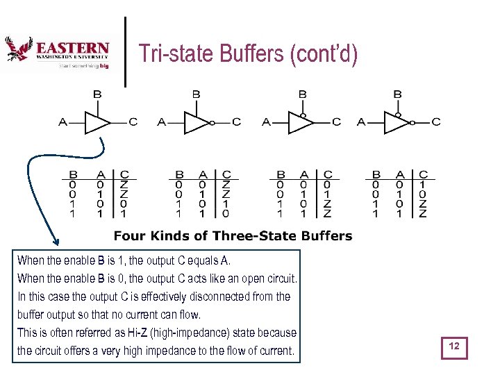
Tri-state Buffers (cont’d) When the enable B is 1, the output C equals A. When the enable B is 0, the output C acts like an open circuit. In this case the output C is effectively disconnected from the buffer output so that no current can flow. This is often referred as Hi-Z (high-impedance) state because the circuit offers a very high impedance to the flow of current. 12
Tri-state Buffers application examples 13
Tri-state Buffers application examples (cont’d) 14
Tri-state buffers application examples (cont’d) 15
Tri-state Buffers application examples (cont’d) 16
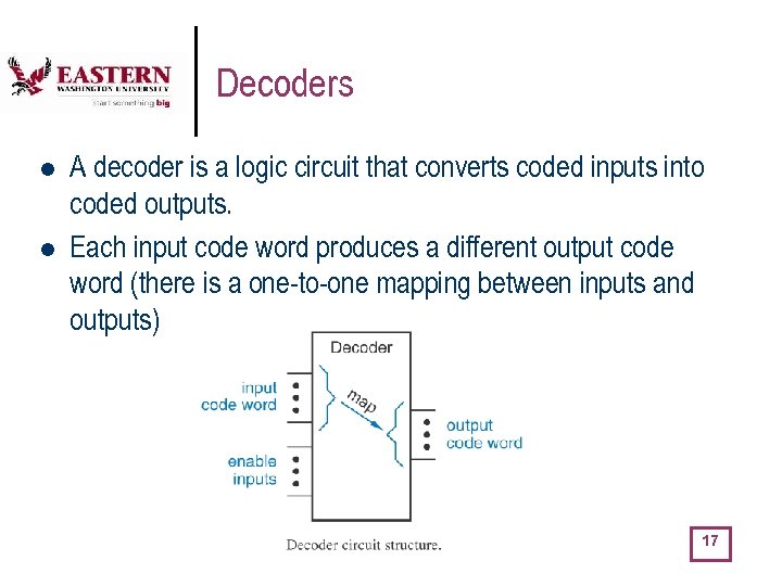
Decoders l l A decoder is a logic circuit that converts coded inputs into coded outputs. Each input code word produces a different output code word (there is a one-to-one mapping between inputs and outputs) 17
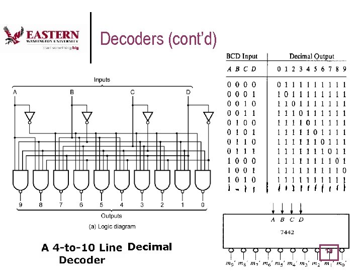
Decoders (cont’d) Decimal 18
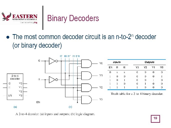
Binary Decoders l The most common decoder circuit is an n-to-2 n decoder (or binary decoder) 19
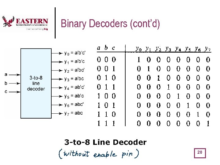
Binary Decoders (cont’d) 20
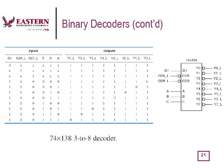
Binary Decoders (cont’d) 21
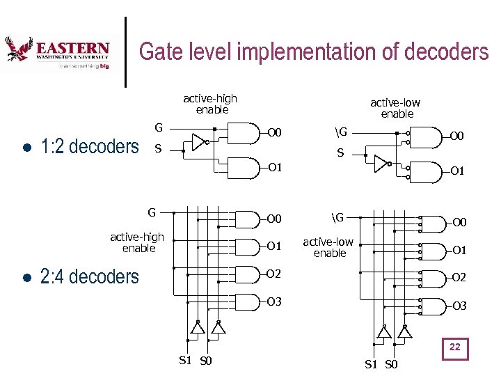
Gate level implementation of decoders active-high enable G l 1: 2 decoders active-low enable O 0 S G O 0 S O 1 G O 0 active-high enable l O 1 2: 4 decoders O 1 G O 0 active-low enable O 1 O 2 O 3 22 S 1 S 0
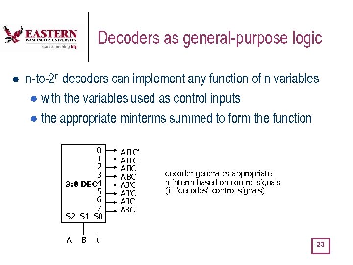
Decoders as general-purpose logic l n-to-2 n decoders can implement any function of n variables l with the variables used as control inputs l the appropriate minterms summed to form the function 0 1 2 3 3: 8 DEC 4 5 6 7 S 2 S 1 S 0 A B C A'B'C' A'B'C A'BC' A'BC AB'C' AB'C ABC' ABC decoder generates appropriate minterm based on control signals (it "decodes" control signals) 23
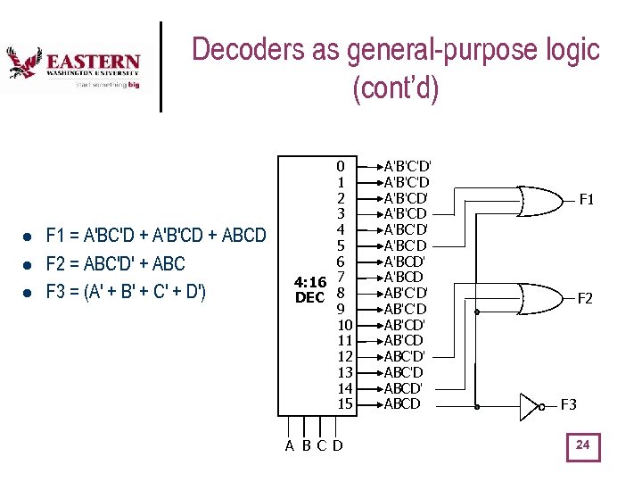
Decoders as general-purpose logic (cont’d) l l l F 1 = A'BC'D + A'B'CD + ABCD F 2 = ABC'D' + ABC F 3 = (A' + B' + C' + D') 0 1 2 3 4 5 6 4: 16 7 DEC 8 9 10 11 12 13 14 15 A B C D A'B'C'D' A'B'C'D A'B'CD' A'B'CD A'BC'D' A'BC'D A'BCD' A'BCD AB'C'D' AB'C'D AB'CD' AB'CD ABC'D' ABC'D ABCD' ABCD F 1 F 2 F 3 24
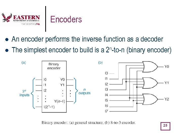
Encoders l l An encoder performs the inverse function as a decoder The simplest encoder to build is a 2 n-to-n (binary encoder) 25
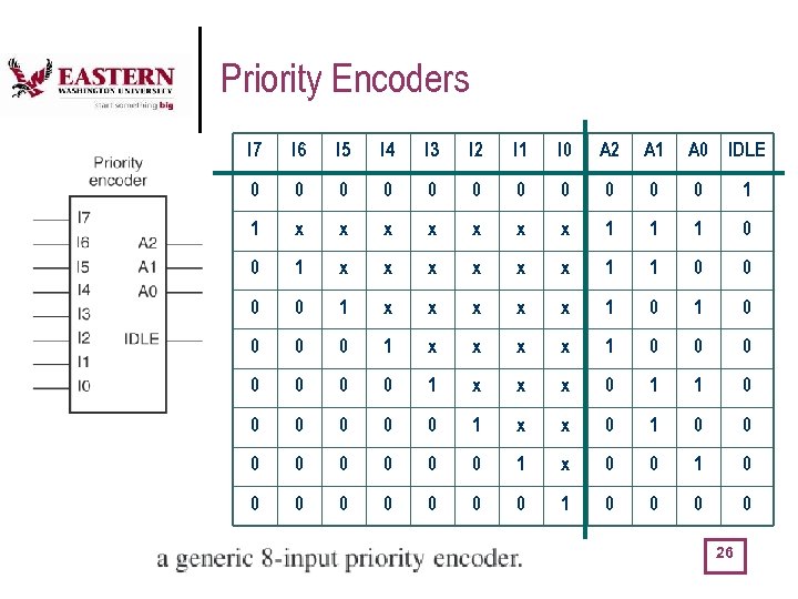
Priority Encoders I 7 I 6 I 5 I 4 I 3 I 2 I 1 I 0 A 2 A 1 A 0 IDLE 0 0 0 1 1 x x x x 1 1 1 0 0 1 x x x 1 0 0 0 0 1 x x x 0 1 1 0 0 0 1 x x 0 1 0 0 0 0 1 x 0 0 1 0 0 26
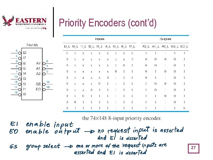
Priority Encoders (cont’d) 27
Programmable Arrays l l l ROM (read only memories) PLA (programmable logic array) PAL (programmable array logic) CPLD (complex programmable logic devices) FPGA (field programmable gate arrays) 28
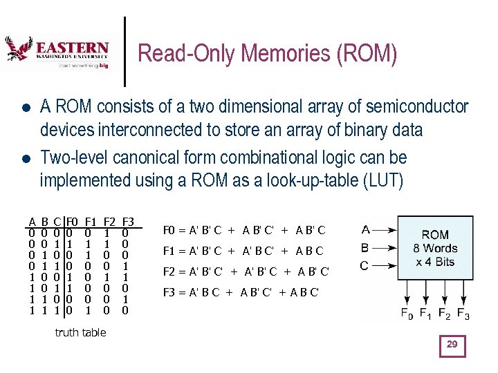
Read-Only Memories (ROM) l l A 0 0 1 1 A ROM consists of a two dimensional array of semiconductor devices interconnected to store an array of binary data Two-level canonical form combinational logic can be implemented using a ROM as a look-up-table (LUT) B 0 0 1 1 C 0 1 0 1 F 0 0 1 1 0 0 F 1 0 1 1 0 0 1 F 2 1 1 0 0 0 F 3 0 0 0 1 1 0 F 0 = A' B' C + A B' C' + A B' C F 1 = A' B' C + A' B C' + A B C F 2 = A' B' C' + A' B' C + A B' C' F 3 = A' B C + A B' C' + A B C' truth table 29
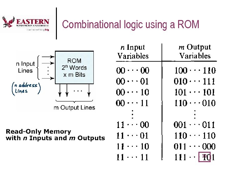
Combinational logic using a ROM 30
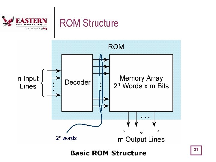
ROM Structure 2 n words 31
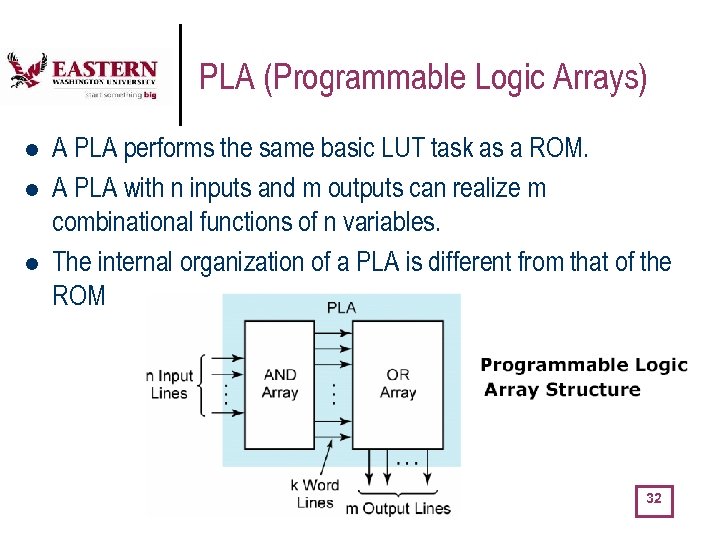
PLA (Programmable Logic Arrays) l l l A PLA performs the same basic LUT task as a ROM. A PLA with n inputs and m outputs can realize m combinational functions of n variables. The internal organization of a PLA is different from that of the ROM 32
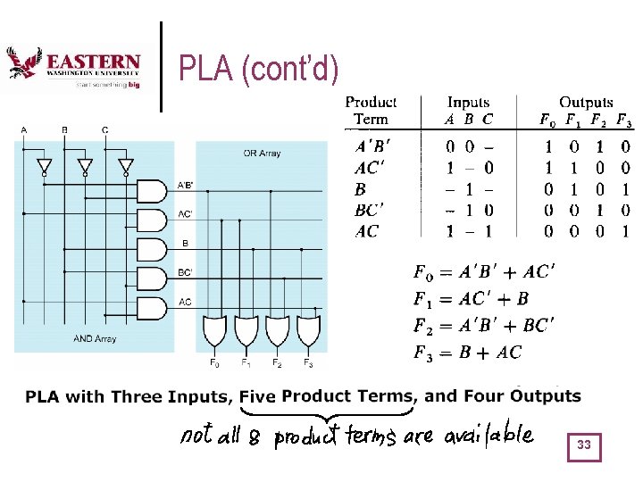
PLA (cont’d) 33
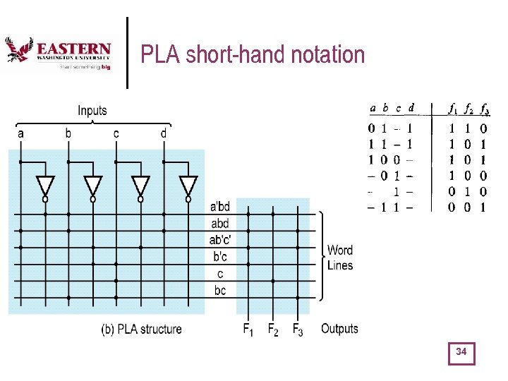
PLA short-hand notation 34
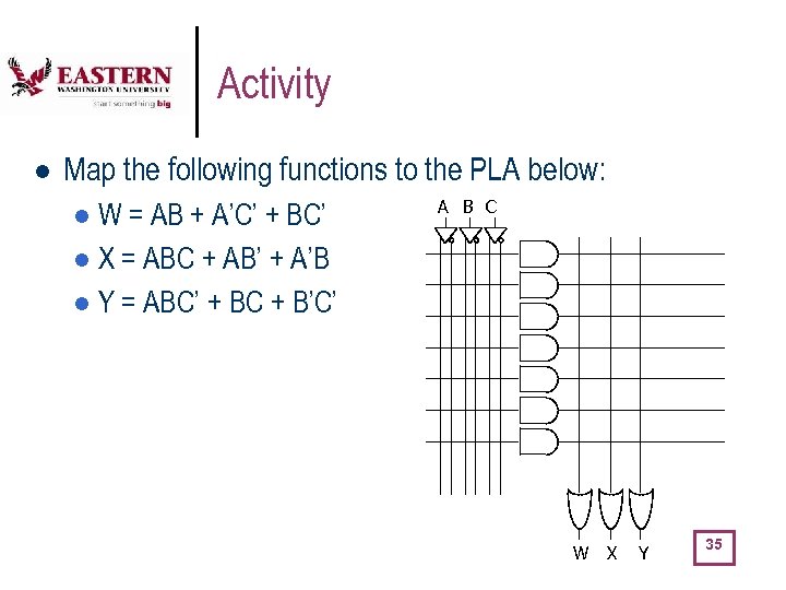
Activity l Map the following functions to the PLA below: W = AB + A’C’ + BC’ l X = ABC + AB’ + A’B l Y = ABC’ + BC + B’C’ l A B C W X Y 35
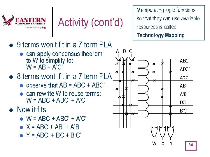
Activity (cont’d) l 9 terms won’t fit in a 7 term PLA l l A B C ABC’ 8 terms wont’ fit in a 7 term PLA l l l can apply concensus theorem to W to simplify to: W = AB + A’C’ Manipulating logic functions so that they can use available resources is called Technology Mapping A’C’ observe that AB = ABC + ABC’ can rewrite W to reuse terms: W = ABC + ABC’ + A’C’ AB’ A’B BC Now it fits l l l B’C’ W = ABC + ABC’ + A’C’ X = ABC + AB’ + A’B Y = ABC’ + BC + B’C’ W X Y 36
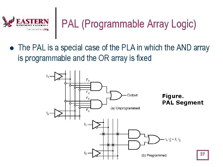
PAL (Programmable Array Logic) l The PAL is a special case of the PLA in which the AND array is programmable and the OR array is fixed Figure. PAL Segment 37
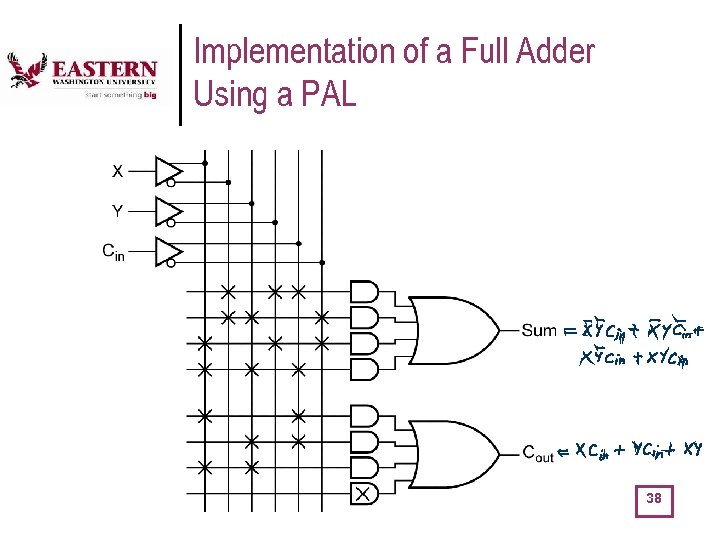
Implementation of a Full Adder Using a PAL 38
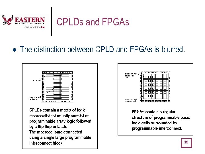
CPLDs and FPGAs l The distinction between CPLD and FPGAs is blurred. CPLDs contain a matrix of logic macrocells that usually consist of programmable array logic followed by a flip-flop or latch. The macrocells are connected using a single large programmable interconnect block FPGAs contain a regular structure of programmable basic logic cells surrounded by programmable interconnect. 39
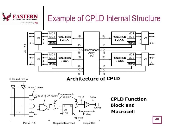
Example of CPLD Internal Structure 40
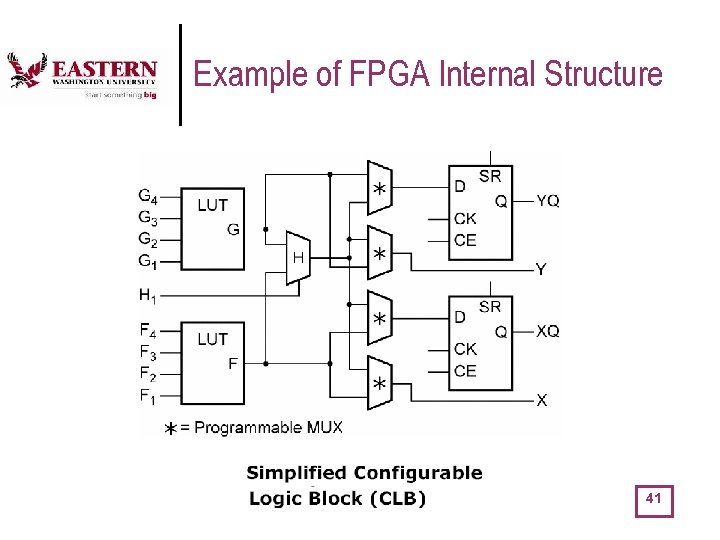
Example of FPGA Internal Structure 41
85481f814e1a536b821a8bc3852114ae.ppt