619425d482f061769dca960ecdd4de30.ppt
- Количество слайдов: 68
 Digital Design Chapter 3: Sequential Logic Design -- Controllers Slides to accompany the textbook Digital Design, with RTL Design, VHDL, and Verilog, 2 nd Edition, by Frank Vahid, John Wiley and Sons Publishers, 2010. http: //www. ddvahid. com Copyright © 2010 Frank Vahid Instructors of courses requiring Vahid's Digital Design textbook (published by John Wiley and Sons) have permission to modify and use these slides for customary course-related activities, subject to keeping this copyright notice in place and unmodified. These slides may be posted as unanimated pdf versions on publicly-accessible course websites. . Power. Point source (or pdf Digital not be 2 e with animations) may Design posted to publicly-accessible websites, but may be posted for students on internal protected sites or distributed directly to students by other electronic means. Copyright © 2010 1 Instructors may make printouts of the slides available to students for a reasonable photocopying charge, without incurring royalties. Any other use requires explicit permission. Instructors Frank Vahid may obtain Power. Point source or obtain special use permissions from Wiley – see http: //www. ddvahid. com for information.
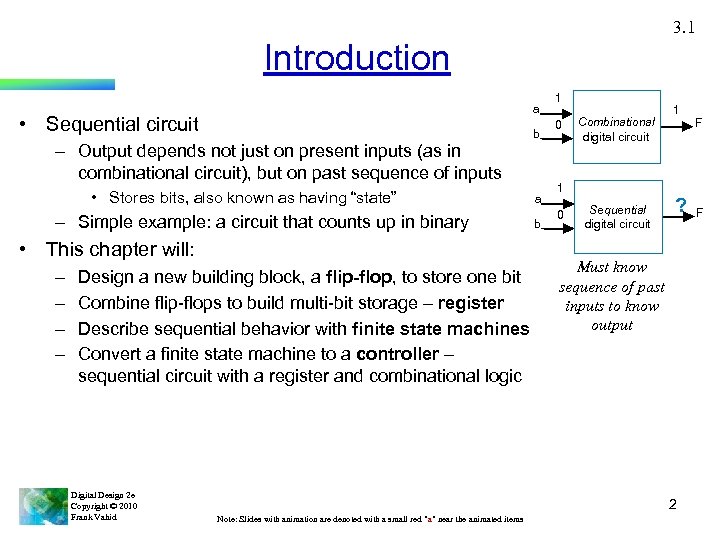 3. 1 Introduction a • Sequential circuit b – Output depends not just on present inputs (as in combinational circuit), but on past sequence of inputs • Stores bits, also known as having “state” – Simple example: a circuit that counts up in binary • This chapter will: – – Design a new building block, a flip-flop, to store one bit Combine flip-flops to build multi-bit storage – register Describe sequential behavior with finite state machines Convert a finite state machine to a controller – sequential circuit with a register and combinational logic Digital Design 2 e Copyright © 2010 Frank Vahid a b 1 0 Combinational digital circuit 1 0 Sequential digital circuit 1 ? Must know sequence of past inputs to know output 2 Note: Slides with animation are denoted with a small red "a" near the animated items F F
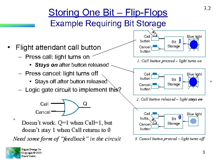 3. 2 Storing One Bit – Flip-Flops Example Requiring Bit Storage Call button • Flight attendant call button – Press call: light turns on • Stays on after button released – Press cancel: light turns off • Stays off after button released – Logic gate circuit to implement this? Call Q Cancel a Doesn’t work. Q=1 when Call=1, but doesn’t stay 1 when Call returns to 0 Need some form of “feedback” in the circuit Digital Design 2 e Copyright © 2010 Frank Vahid Cancel button 1 Blue light Bit Storage 1. Call button pressed – light turns on Call button Cancel button 1 Blue light Bit Storage a 2. Call button released – light stays on Call button Cancel button 0 Blue light Bit Storage 3. Cancel button pressed – light turns off 3
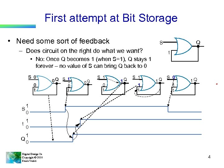 First attempt at Bit Storage • Need some sort of feedback Q S – Does circuit on the right do what we want? t • No: Once Q becomes 1 (when S=1), Q stays 1 forever – no value of S can bring Q back to 0 S 1 0 t S 0 t 1 Q S 1 1 t 1 Q S 0 1 t 1 Q a 1 0 Q S 1 1 0 t 0 Q 1 0 Digital Design 2 e Copyright © 2010 Frank Vahid 4
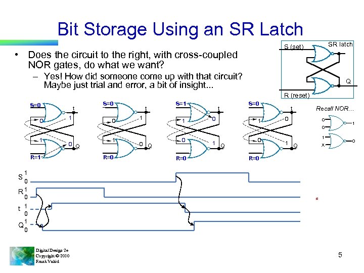 Bit Storage Using an SR Latch SR latch S (set) • Does the circuit to the right, with cross-coupled NOR gates, do what we want? – Yes! How did someone come up with that circuit? Maybe just trial and error, a bit of insight. . . Q R (reset) S=0 0 t 1 S=1 1 S=0 t 0 1 t Recall NOR… 0 0 1 0 Q R=1 1 0 R 1 0 t 1 0 1 Q 0 1 R=0 0 Q 0 R=0 1 Q 0 1 1 0 X Q R=0 S a Digital Design 2 e Copyright © 2010 Frank Vahid 5
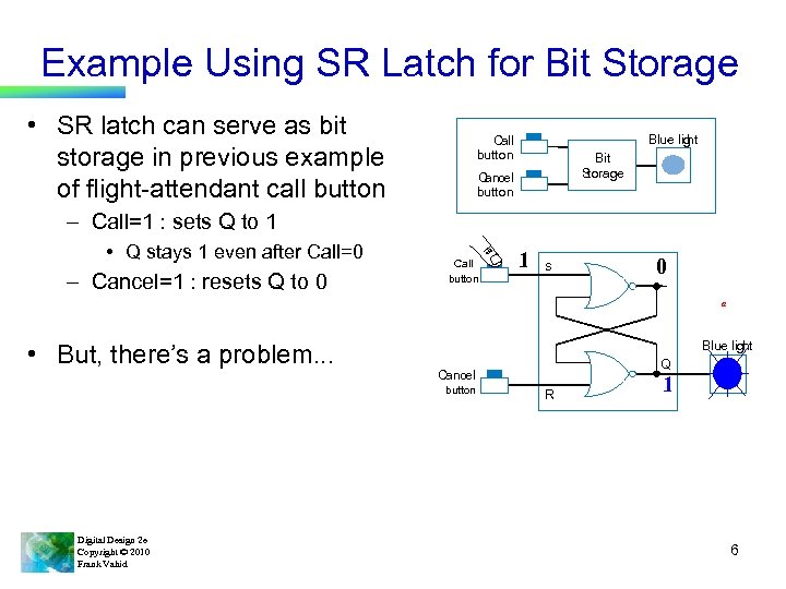 Example Using SR Latch for Bit Storage • SR latch can serve as bit storage in previous example of flight-attendant call button Blue lig ht Call button Bit Storage Cancel button – Call=1 : sets Q to 1 • Q stays 1 even after Call=0 – Cancel=1 : resets Q to 0 Call button 1 S 0 a • But, there’s a problem. . . Blue light button Digital Design 2 e Copyright © 2010 Frank Vahid Q Cancel R 1 6
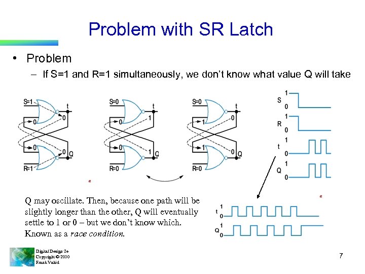 Problem with SR Latch • Problem – If S=1 and R=1 simultaneously, we don’t know what value Q will take a Q may oscillate. Then, because one path will be slightly longer than the other, Q will eventually settle to 1 or 0 – but we don’t know which. Known as a race condition. Digital Design 2 e Copyright © 2010 Frank Vahid a 7
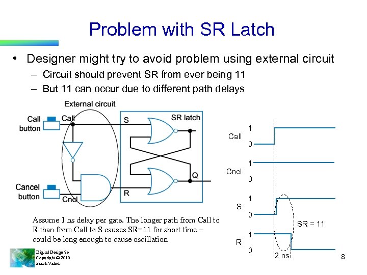 Problem with SR Latch • Designer might try to avoid problem using external circuit – Circuit should prevent SR from ever being 11 – But 11 can occur due to different path delays Call Cncl S Assume 1 ns delay per gate. The longer path from Call to R than from Call to S causes SR=11 for short time – could be long enough to cause oscillation Digital Design 2 e Copyright © 2010 Frank Vahid 1 0 1 0 SR = 11 R 1 0 2 ns 8
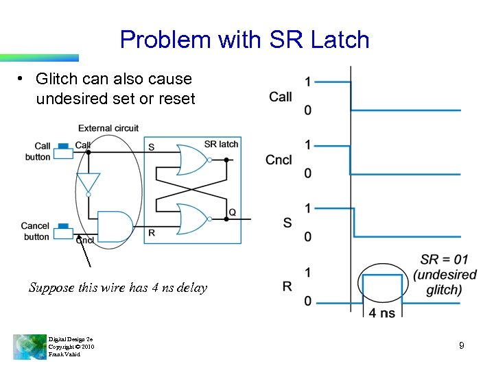 Problem with SR Latch • Glitch can also cause undesired set or reset Suppose this wire has 4 ns delay Digital Design 2 e Copyright © 2010 Frank Vahid 9
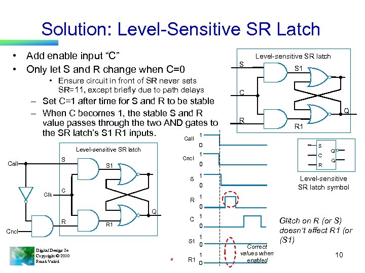 Solution: Level-Sensitive SR Latch • Add enable input “C” • Only let S and R change when C=0 Level-sensitive SR latch S • Ensure circuit in front of SR never sets SR=11, except briefly due to path delays – Set C=1 after time for S and R to be stable – When C becomes 1, the stable S and R value passes through the two AND gates to the SR latch’s S 1 R 1 inputs. 1 Call Level-sensitive SR latch S Call Cncl S 1 S Clk R Q R C R 1 Cncl S 1 Digital Design 2 e Copyright © 2010 Frank Vahid C Q R a R 1 0 S 1 C 0 R 1 Q’ Q Level-sensitive SR latch symbol 0 C S 1 1 0 1 0 1 R 1 0 Correct values when enabled Glitch on R (or S) doesn’t affect R 1 (or (S 1) 10
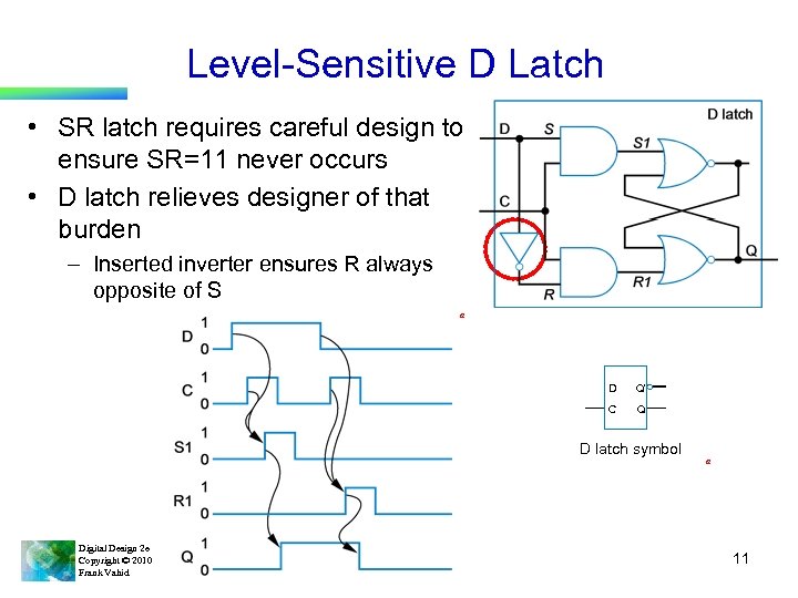 Level-Sensitive D Latch • SR latch requires careful design to ensure SR=11 never occurs • D latch relieves designer of that burden – Inserted inverter ensures R always opposite of S a D Q’ C Q D latch symbol Digital Design 2 e Copyright © 2010 Frank Vahid a 11
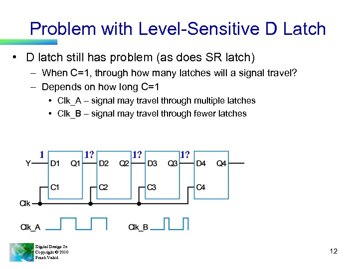 Problem with Level-Sensitive D Latch • D latch still has problem (as does SR latch) – When C=1, through how many latches will a signal travel? – Depends on how long C=1 • Clk_A – signal may travel through multiple latches • Clk_B – signal may travel through fewer latches 1 Digital Design 2 e Copyright © 2010 Frank Vahid 1? 1? 12
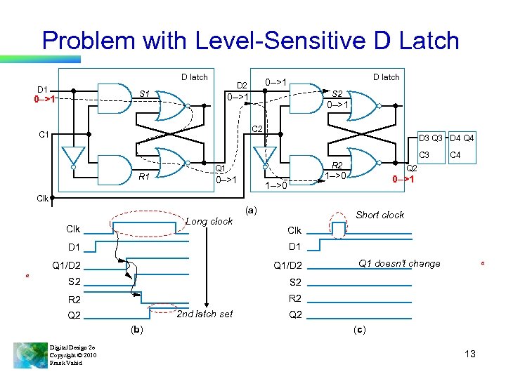 Problem with Level-Sensitive D Latch D latch D 1 S 1 0–>1 D latch 0–>1 D 2 S 2 0–>1 C 2 C 1 D 3 Q 3 D 4 Q 4 C 3 R 1 R 2 Q 1 0–>1 Q 2 1–>0 C 4 0–>1 Clk Long clock Clk (a) Short clock Clk D 1 Q 1/D 2 a D 1 Q 1/D 2 S 2 R 2 2 nd latch set Q 2 (b) Digital Design 2 e Copyright © 2010 Frank Vahid Q 1 doesn't change a Q 2 (c) 13
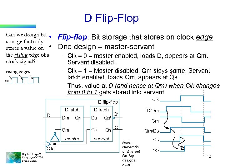 D Flip-Flop Can we design bit • storage that only stores a value on • the rising edge of a clock signal? rising edges Flip-flop: Bit storage that stores on clock edge One design – master-servant – Clk = 0 – master enabled, loads D, appears at Qm. Servant disabled. – Clk = 1 – Master disabled, Qm stays same. Servant latch enabled, loads Qm, appears at Qs. – Thus, value at D (and hence at Qm) when Clk changes from 0 to 1 gets stored into servant a Clk D flip-flop D latch D Dm Qm Cm master Clk Digital Design 2 e Copyright © 2010 Frank Vahid D latch Ds Qs¢ Cs Qs servant D/Dm Q¢ Cm Q Qm/Ds Note: Hundreds of different flip-flop designs exist Cs Qs 14
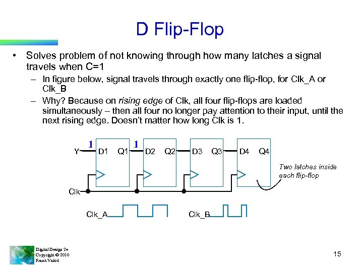 D Flip-Flop • Solves problem of not knowing through how many latches a signal travels when C=1 – In figure below, signal travels through exactly one flip-flop, for Clk_A or Clk_B – Why? Because on rising edge of Clk, all four flip-flops are loaded simultaneously – then all four no longer pay attention to their input, until the next rising edge. Doesn’t matter how long Clk is 1. Y 1 D 1 Q 1 1 D 2 Q 2 D 3 Q 3 D 4 Q 4 Two latches inside each flip-flop Clk_A Digital Design 2 e Copyright © 2010 Frank Vahid Clk_B 15
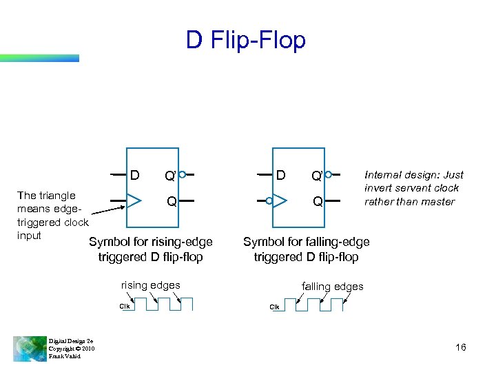 D Flip-Flop D The triangle means edgetriggered clock input Q’ D Q Symbol for rising-edge triggered D flip-flop Q Digital Design 2 e Copyright © 2010 Frank Vahid Internal design: Just invert servant clock rather than master Symbol for falling-edge triggered D flip-flop rising edges Clk Q’ falling edges Clk 16
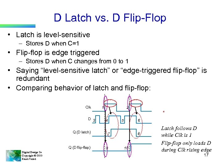 D Latch vs. D Flip-Flop • Latch is level-sensitive – Stores D when C=1 • Flip-flop is edge triggered – Stores D when C changes from 0 to 1 • Saying “level-sensitive latch” or “edge-triggered flip-flop” is redundant • Comparing behavior of latch and flip-flop: Clk 1 2 a D 3 Q (D latch) Q (D flip-flop) Digital Design 2 e Copyright © 2010 Frank Vahid 4 5 6 7 9 8 10 Latch follows D while Clk is 1 Flip-flop only loads D during Clk rising edge 17
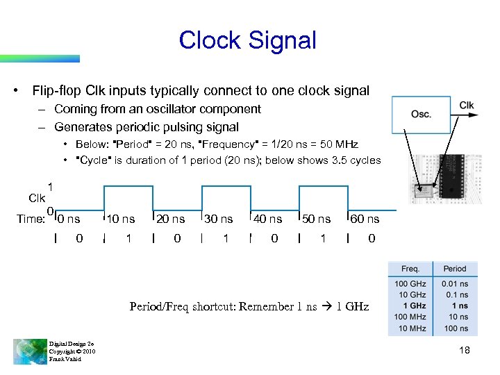 Clock Signal • Flip-flop Clk inputs typically connect to one clock signal – Coming from an oscillator component – Generates periodic pulsing signal • Below: "Period" = 20 ns, "Frequency" = 1/20 ns = 50 MHz • "Cycle" is duration of 1 period (20 ns); below shows 3. 5 cycles Clk Time: 1 0 0 ns 10 ns 0 1 20 ns 0 30 ns 1 40 ns 0 50 ns 1 60 ns 0 Period/Freq shortcut: Remember 1 ns 1 GHz Digital Design 2 e Copyright © 2010 Frank Vahid 18
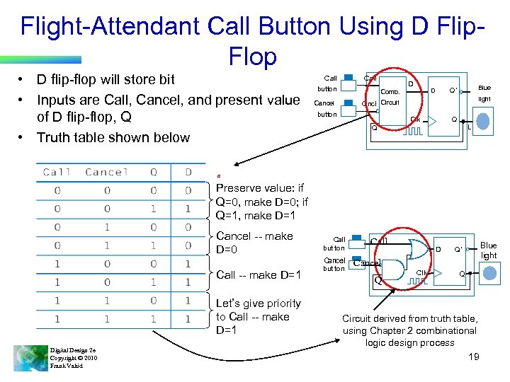 Flight-Attendant Call Button Using D Flip. Flop • D flip-flop will store bit • Inputs are Call, Cancel, and present value of D flip-flop, Q • Truth table shown below Call button D Blue Q¢ D Comb. light Cncl Circuit Cancel button Clk Q L Q a Preserve value: if Q=0, make D=0; if Q=1, make D=1 Cancel -- make D=0 Call but ton Cancel Call -- make D=1 Let’s give priority to Call -- make D=1 Digital Design 2 e Copyright © 2010 Frank Vahid but ton Call D Q’ Cancel Q Clk Q Circuit derived from truth table, using Chapter 2 combinational logic design process 19 Blue light
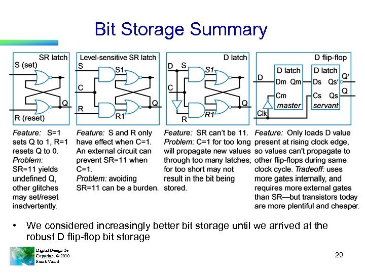 Bit Storage Summary • We considered increasingly better bit storage until we arrived at the robust D flip-flop bit storage Digital Design 2 e Copyright © 2010 Frank Vahid 20
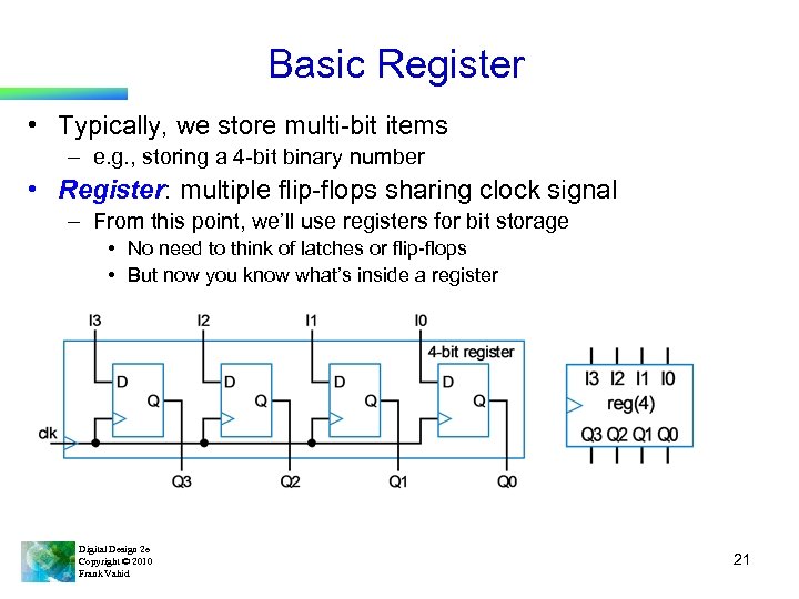 Basic Register • Typically, we store multi-bit items – e. g. , storing a 4 -bit binary number • Register: multiple flip-flops sharing clock signal – From this point, we’ll use registers for bit storage • No need to think of latches or flip-flops • But now you know what’s inside a register Digital Design 2 e Copyright © 2010 Frank Vahid 21
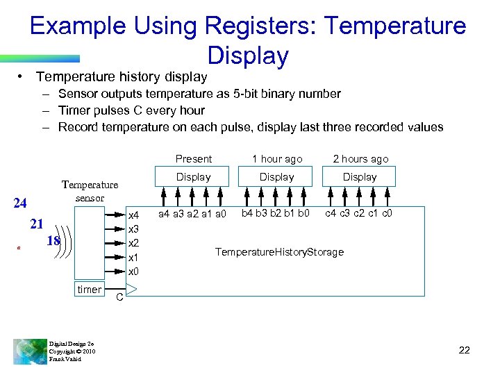 Example Using Registers: Temperature Display • Temperature history display – Sensor outputs temperature as 5 -bit binary number – Timer pulses C every hour – Record temperature on each pulse, display last three recorded values Present 24 x 3 x 2 x 1 x 0 21 a 18 timer Digital Design 2 e Copyright © 2010 Frank Vahid 2 hours ago Display Temperature sensor 1 hour ago Display a 4 a 3 a 2 a 1 a 0 b 4 b 3 b 2 b 1 b 0 c 4 c 3 c 2 c 1 c 0 Temperature. History. Storage C 22
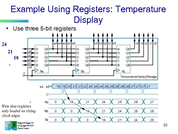 Example Using Registers: Temperature Display • Use three 5 -bit registers 24 a 3 a 2 a 1 a 0 21 x 4 x 3 x 2 x 1 x 0 18 a I 4 I 3 I 2 I 1 I 0 Q 4 Q 3 Q 2 Q 1 Q 0 I 4 I 3 I 2 I 1 I 0 Ra C b 4 b 3 b 2 b 1 b 0 Q 4 Q 3 Q 2 Q 1 Q 0 c 4 c 3 c 2 c 1 c 0 I 4 I 3 I 2 I 1 I 0 Q 4 Q 3 Q 2 Q 1 Q 0 Rb Rc Temperature. History. Storage x 4. . . x 0 15 18 20 21 21 22 24 24 24 25 25 26 26 26 27 27 C a Note that registers only loaded on rising clock edges Digital Design 2 e Copyright © 2010 Frank Vahid Ra 0 18 21 24 25 26 27 Rb 0 0 18 21 24 25 26 Rc 0 0 0 18 21 24 25 23
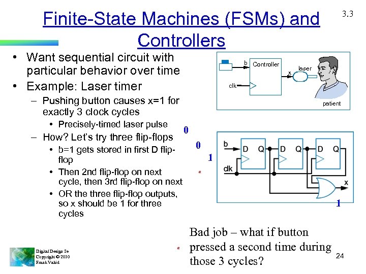 Finite-State Machines (FSMs) and Controllers • Want sequential circuit with particular behavior over time • Example: Laser timer b Controller x patient 0 – How? Let’s try three flip-flops • b=1 gets stored in first D flipflop • Then 2 nd flip-flop on next cycle, then 3 rd flip-flop on next • OR the three flip-flop outputs, so x should be 1 for three cycles Digital Design 2 e Copyright © 2010 Frank Vahid laser clk – Pushing button causes x=1 for exactly 3 clock cycles • Precisely-timed laser pulse 3. 3 a 0 1 a 1 Bad job – what if button pressed a second time during those 3 cycles? 24
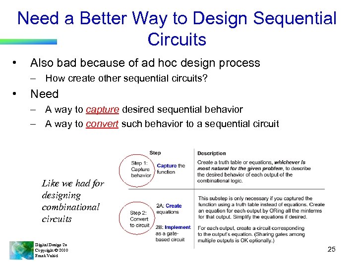 Need a Better Way to Design Sequential Circuits • Also bad because of ad hoc design process – How create other sequential circuits? • Need – A way to capture desired sequential behavior – A way to convert such behavior to a sequential circuit Like we had for designing combinational circuits Digital Design 2 e Copyright © 2010 Frank Vahid 25
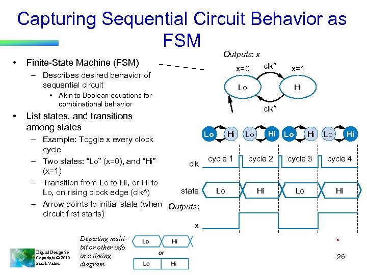 Capturing Sequential Circuit Behavior as FSM • Outputs: x Finite-State Machine (FSM) x=0 – Describes desired behavior of sequential circuit List states, and transitions among states – Example: Toggle x every clock cycle – Two states: “Lo” (x=0), and “Hi” clk (x=1) – Transition from Lo to Hi, or Hi to state Lo, on rising clock edge (clk^) – Arrow points to initial state (when Outputs: circuit first starts) x Digital Design 2 e Copyright © 2010 Frank Vahid Depicting multibit or other info in a timing diagram x=1 Lo • Akin to Boolean equations for combinational behavior • clk^ Hi clk^ Lo Hi Hi Lo cycle 1 cycle 2 cycle 3 cycle 4 Lo Hi a 26
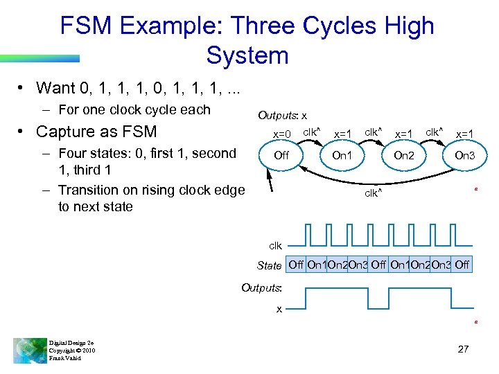 FSM Example: Three Cycles High System • Want 0, 1, 1, 1, . . . – For one clock cycle each Outputs: x • Capture as FSM x=0 – Four states: 0, first 1, second 1, third 1 – Transition on rising clock edge to next state Off clk^ x=1 clk^ On 1 x=1 On 2 clk^ x=1 On 3 a clk^ clk State Off On 1 On 2 On 3 Off Outputs: x a Digital Design 2 e Copyright © 2010 Frank Vahid 27
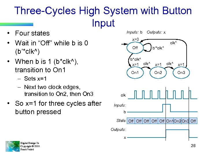 Three-Cycles High System with Button Input • Four states • Wait in “Off” while b is 0 (b’*clk^) • When b is 1 (b*clk^), transition to On 1 – Sets x=1 – Next two clock edges, transition to On 2, then On 3 • So x=1 for three cycles after button pressed Inputs: b Outputs: x x=0 Off clk^ b'*clk ^ b*clk ^ x=1 clk^ x=1 On 2 clk^ x=1 On 3 clk Inputs: b State Off Off Off On 1 On 2 On 3 Off Outputs: x Digital Design 2 e Copyright © 2010 Frank Vahid 28
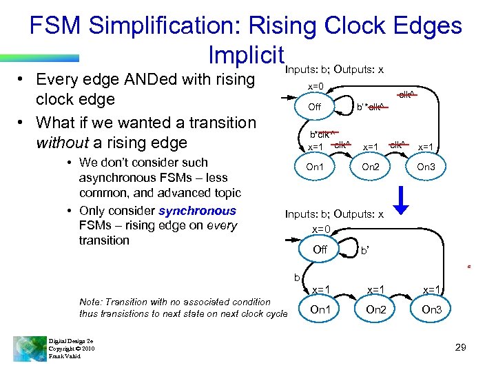 FSM Simplification: Rising Clock Edges Implicit. Inputs: b; Outputs: x • Every edge ANDed with rising clock edge • What if we wanted a transition without a rising edge • We don’t consider such asynchronous FSMs – less common, and advanced topic • Only consider synchronous FSMs – rising edge on every transition x=0 Off clk^ b’ *clk^ b*clk ^ x=1 clk^ x=1 On 2 clk^ x=1 On 3 Inputs: b; Outputs: x x=0 Off b’ a b x=1 Note: Transition with no associated condition thus transistions to next state on next clock cycle Digital Design 2 e Copyright © 2010 Frank Vahid x=1 On 2 On 3 29
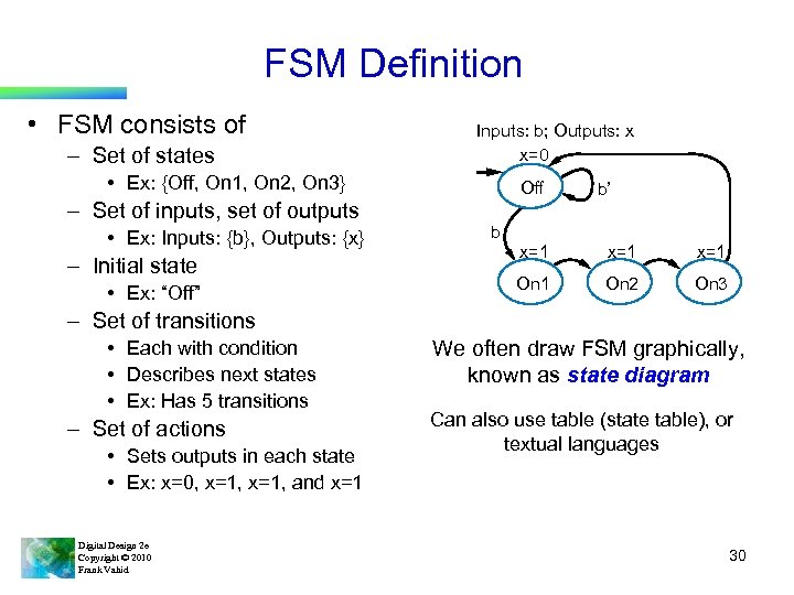 FSM Definition • FSM consists of – Set of states Inputs: b; Outputs: x x=0 • Ex: {Off, On 1, On 2, On 3} – Set of inputs, set of outputs • Ex: Inputs: {b}, Outputs: {x} – Initial state • Ex: “Off” Off b’ b x=1 x=1 On 2 On 3 – Set of transitions • Each with condition • Describes next states • Ex: Has 5 transitions – Set of actions • Sets outputs in each state • Ex: x=0, x=1, and x=1 Digital Design 2 e Copyright © 2010 Frank Vahid We often draw FSM graphically, known as state diagram Can also use table (state table), or textual languages 30
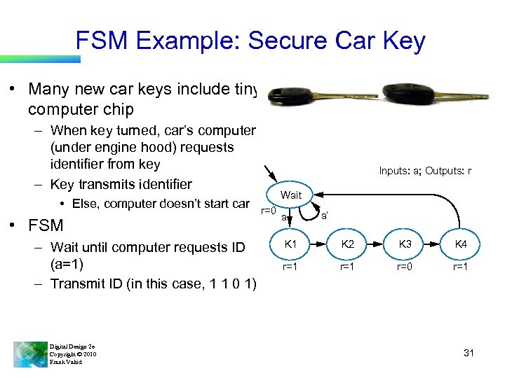 FSM Example: Secure Car Key • Many new car keys include tiny computer chip – When key turned, car’s computer (under engine hood) requests identifier from key – Key transmits identifier • Else, computer doesn’t start car • FSM – Wait until computer requests ID (a=1) – Transmit ID (in this case, 1 1 0 1) Digital Design 2 e Copyright © 2010 Frank Vahid Inputs: a; Outputs: r Wait r=0 a a’ K 1 K 2 K 3 K 4 r=1 r=0 r=1 31
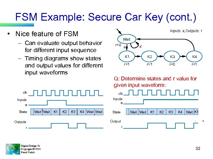 FSM Example: Secure Car Key (cont. ) Inputs: a; Outputs: r • Nice feature of FSM – Can evaluate output behavior for different input sequence – Timing diagrams show states and output values for different input waveforms clk r=0 a a’ K 1 K 2 K 3 K 4 r=1 r=0 r=1 Q: Determine states and r value for given input waveform: clk Inputs a State Wait Outputs r Digital Design 2 e Copyright © 2010 Frank Vahid K 1 K 2 K 3 K 4 Wait State Wait K 1 K 2 K 3 K 4 Wait K 1 Output a r 32
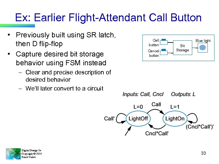 Ex: Earlier Flight-Attendant Call Button • Previously built using SR latch, then D flip-flop • Capture desired bit storage behavior using FSM instead Call button Cancel button Blue light Bit Storage – Clear and precise description of desired behavior – We’ll later convert to a circuit Digital Design 2 e Copyright © 2010 Frank Vahid 33
 How To Capture Desired Behavior as FSM • List states – Give meaningful names, show initial state – Optionally add some transitions if they help • Create transitions – For each state, define all possible transitions leaving that state. • Refine the FSM – Execute the FSM mentally and make any needed improvements. Digital Design 2 e Copyright © 2010 Frank Vahid 34
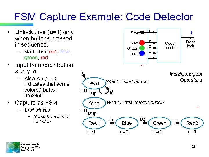 FSM Capture Example: Code Detector • Unlock door (u=1) only when buttons pressed in sequence: • Input from each button: s, r, g, b • Capture as FSM – List states • Some transitions included r g b a Code detector 1 Door lock a Wait u=0 s Start Inputs: s, r, g, b, a Outputs: u Wait for start button s' Wait for first colored button a u=0 ar Red 1 u=0 Digital Design 2 e Copyright © 2010 Frank Vahid u Red Green Blue – start, then red, blue, green, red – Also, output a indicates that some colored button pressed s Start ab Blue u=0 ag Green u=0 ar Red 2 u=1 35
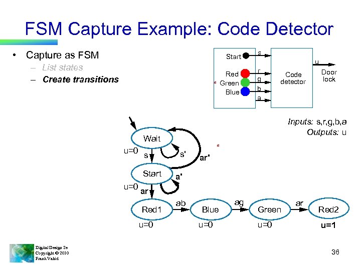 FSM Capture Example: Code Detector • Capture as FSM Start – List states – Create transitions Red Green Blue a s u r g b a Code detector Inputs: s, r, g, b, a Outputs: u Wait u=0 s Start Door lock a s' ar' a' u=0 ar Red 1 u=0 Digital Design 2 e Copyright © 2010 Frank Vahid ab Blue u=0 ag Green u=0 ar Red 2 u=1 36
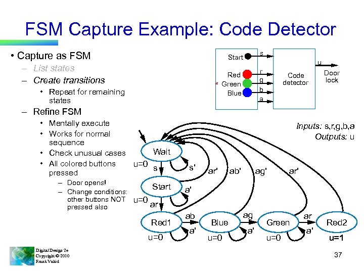 FSM Capture Example: Code Detector • Capture as FSM s Start – List states – Create transitions a • Repeat for remaining states u r g b a Red Green Blue Code detector Door lock – Refine FSM • Mentally execute • Works for normal sequence Wait • Check unusual cases • All colored buttons u=0 s pressed – Door opens! Start – Change conditions: other buttons NOT u=0 ar pressed also Red 1 u=0 Digital Design 2 e Copyright © 2010 Frank Vahid Inputs: s, r, g, b, a Outputs: u s' ar' ab' ag' ar' a' ab a' Blue u=0 ag a' Green u=0 ar a' Red 2 u=1 37
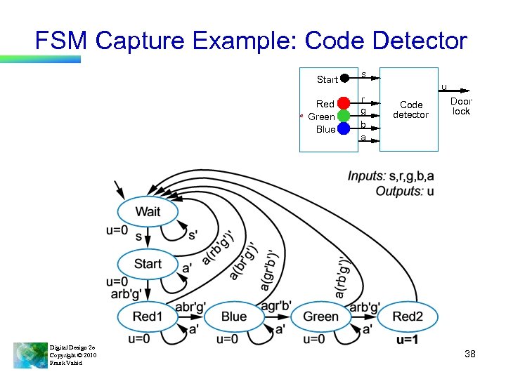 FSM Capture Example: Code Detector Start a Digital Design 2 e Copyright © 2010 Frank Vahid Red Green Blue s u r g b a Code detector Door lock 38
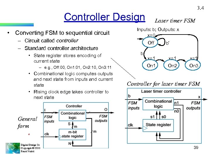 3. 4 Controller Design • Converting FSM to sequential circuit – Circuit called controller – Standard controller architecture • State register stores encoding of current state – e. g. , Off: 00, On 1: 01, On 2: 10, On 3: 11 • Combinational logic computes outputs and next state from inputs and current state • Rising clock edge takes controller to next state Laser timer FSM Inputs: b; Outputs: x x=0 Off b b’ x=1 x=1 On 2 On 3 Controller for laser timer FSM General form a Digital Design 2 e Copyright © 2010 Frank Vahid 39
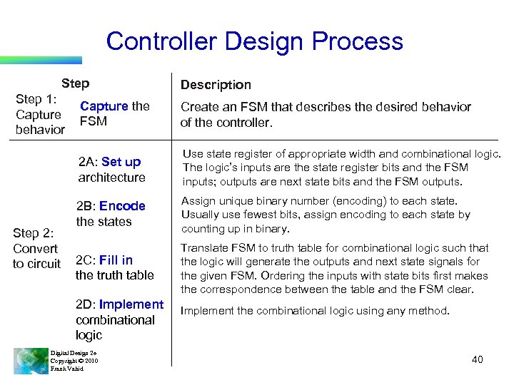 Controller Design Process Step 1: Capture behavior Description Create an FSM that describes the desired behavior of the controller. 2 A: Set up architecture Step 2: Convert to circuit Capture the FSM Use state register of appropriate width and combinational logic. The logic’s inputs are the state register bits and the FSM inputs; outputs are next state bits and the FSM outputs. 2 B: Encode the states Assign unique binary number (encoding) to each state. Usually use fewest bits, assign encoding to each state by counting up in binary. 2 C: Fill in the truth table Translate FSM to truth table for combinational logic such that the logic will generate the outputs and next state signals for the given FSM. Ordering the inputs with state bits first makes the correspondence between the table and the FSM clear. 2 D: Implement combinational logic Digital Design 2 e Copyright © 2010 Frank Vahid Implement the combinational logic using any method. 40
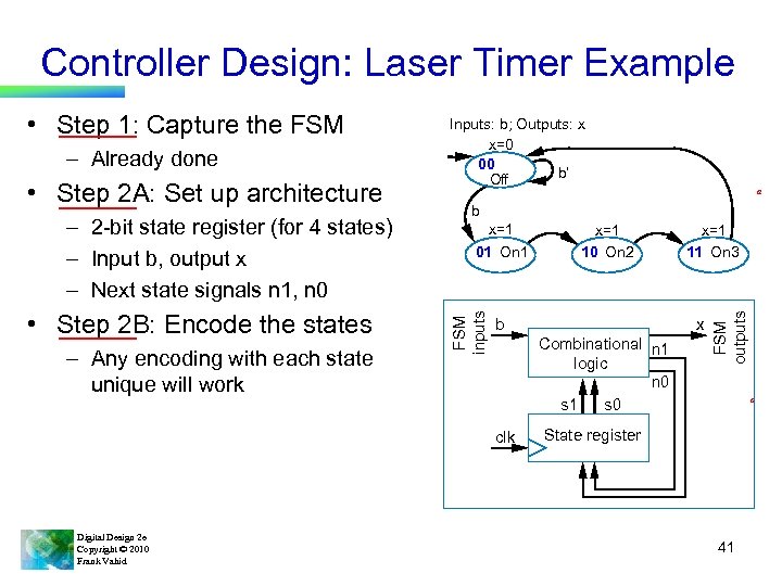 Controller Design: Laser Timer Example • Step 2 A: Set up architecture – 2 -bit state register (for 4 states) – Input b, output x – Next state signals n 1, n 0 • Step 2 B: Encode the states – Any encoding with each state unique will work b x=1 01 On 1 x=1 10 On 2 x=1 11 On 3 x b Combinational n 1 logic n 0 s 1 s 0 clk Digital Design 2 e Copyright © 2010 Frank Vahid a FSM outputs – Already done Inputs: b; Outputs: x x=0 00 b’ Off FSM inputs • Step 1: Capture the FSM a State register 41
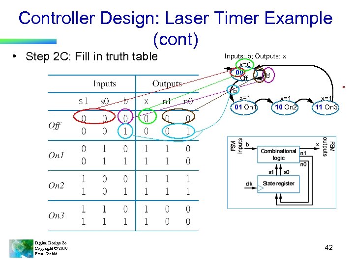 Controller Design: Laser Timer Example (cont) • Step 2 C: Fill in truth table Inputs: b; Outputs: x x=0 00 b’ Off b x=1 01 On 1 Digital Design 2 e Copyright © 2010 Frank Vahid a x=1 10 On 2 x=1 11 On 3 42
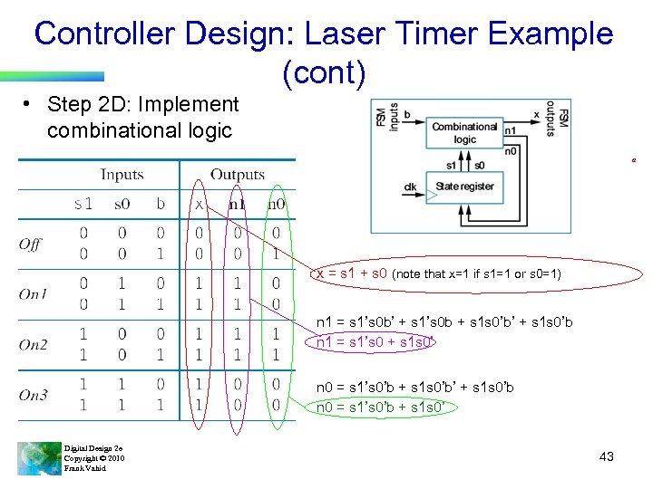 Controller Design: Laser Timer Example (cont) • Step 2 D: Implement combinational logic a x = s 1 + s 0 (note that x=1 if s 1=1 or s 0=1) n 1 = s 1’s 0 b’ + s 1’s 0 b + s 1 s 0’b’ + s 1 s 0’b n 1 = s 1’s 0 + s 1 s 0’ n 0 = s 1’s 0’b + s 1 s 0’b’ + s 1 s 0’b n 0 = s 1’s 0’b + s 1 s 0’ Digital Design 2 e Copyright © 2010 Frank Vahid 43
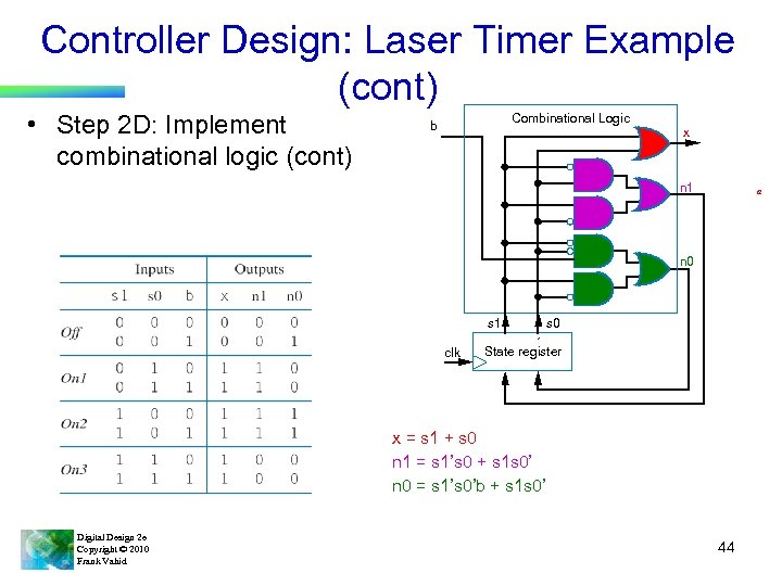 Controller Design: Laser Timer Example (cont) • Step 2 D: Implement combinational logic (cont) Combinational Logic b x n 1 a n 0 s 1 clk s 0 State register x = s 1 + s 0 n 1 = s 1’s 0 + s 1 s 0’ n 0 = s 1’s 0’b + s 1 s 0’ Digital Design 2 e Copyright © 2010 Frank Vahid 44
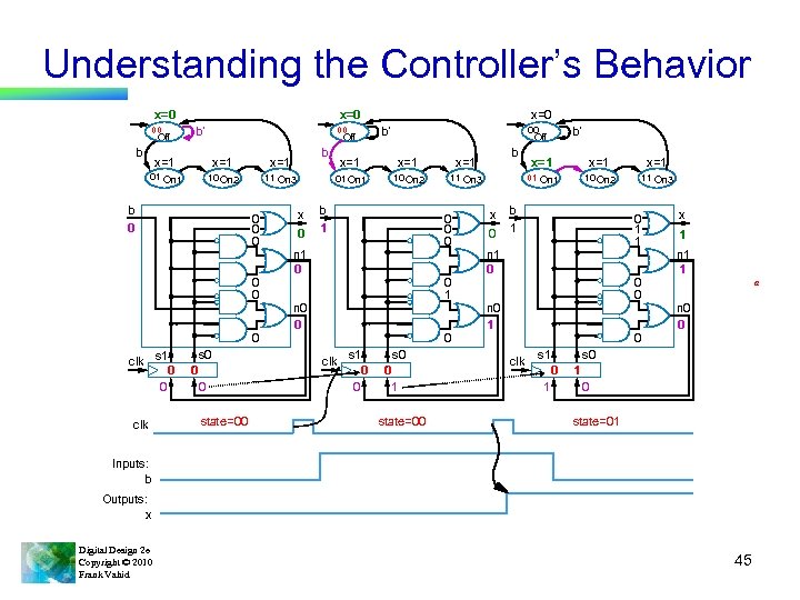 Understanding the Controller’s Behavior x=0 00 Off b b’ b x=1 x=1 01 On 1 10 On 2 11 On 3 b 0 0 0 0 clk s 1 0 0 x=0 00 Off s 0 0 0 state=00 00 Off b’ 0 x=1 10 On 2 b 11 On 3 b 1 0 0 0 n 1 0 0 1 n 0 0 0 clk s 1 0 0 s 0 0 1 state=00 x 0 x=1 x=1 01 On 1 x x=1 b’ 10 On 2 11 On 3 b 1 0 1 1 n 1 0 0 0 n 0 1 0 clk s 1 1 n 1 1 a n 0 0 s 0 0 1 x 1 0 state=01 Inputs: b Outputs: x Digital Design 2 e Copyright © 2010 Frank Vahid 45
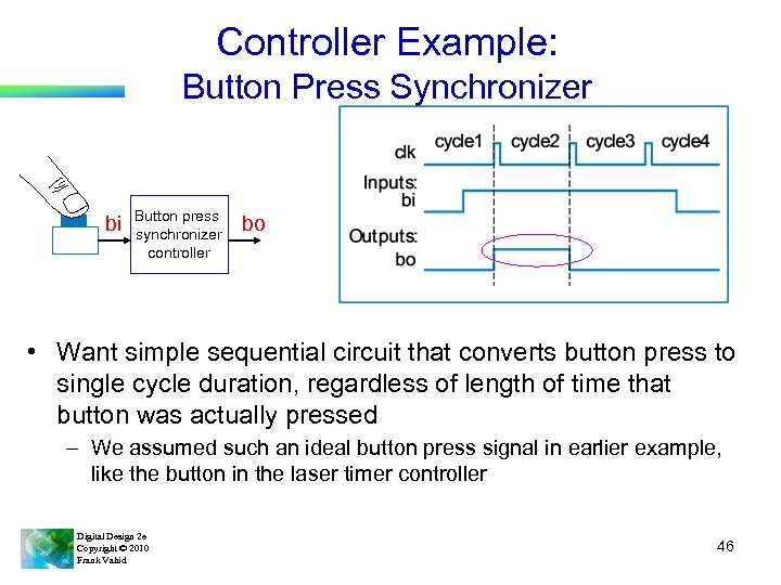 Controller Example: Button Press Synchronizer bi Button press synchronizer controller bo • Want simple sequential circuit that converts button press to single cycle duration, regardless of length of time that button was actually pressed – We assumed such an ideal button press signal in earlier example, like the button in the laser timer controller Digital Design 2 e Copyright © 2010 Frank Vahid 46
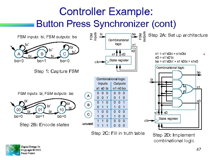 Controller Example: bi’ A bi bo=0 B bi’ bi bo=1 bi C bi’ bo=0 bi bo Combinational logic s 1 clk s 0 FSM outputs FSM inputs: bi; FSM outputs: bo FSM inputs Button Press Synchronizer (cont) Step 2 A: Set up architecture n 1 n 0 n 1 = s 1’s 0 bi + s 1 s 0 bi n 0 = s 1’s 0’bi bo = s 1’s 0 bi’ + s 1’s 0 bi = s 1 s 0 State register Combinational logic Step 1: Capture FSM bo bi n 1 FSM inputs: bi; FSM outputs: bo bi’ 00 bi bo=0 01 bo=1 bi’ bi n 0 bi 10 bi’ s 1 bo=0 Step 2 B: Encode states clk Step 2 C: Fill in truth table Digital Design 2 e Copyright © 2010 Frank Vahid s 0 State register Step 2 D: Implement combinational logic 47 a
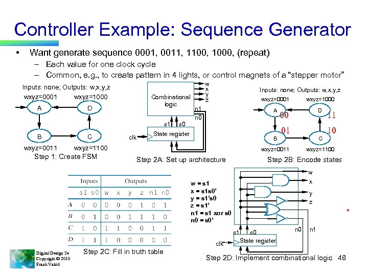 Controller Example: Sequence Generator • Want generate sequence 0001, 0011, 1100, 1000, (repeat) – Each value for one clock cycle – Common, e. g. , to create pattern in 4 lights, or control magnets of a “stepper motor” w x y z Inputs: none; Outputs: w, x, y, z wxyz=0001 wxyz=1000 A D Combinational logic s 1 B C wxyz=0011 s 0 Inputs: none; Outputs: w, x, y, z wxyz=0001 A n 1 n 0 State register wxyz=1100 Step 1: Create FSM clk wxyz=1000 D B 00 01 C wxyz=0011 Step 2 A: Set up architecture Step 2 B: Encode states w x y z a s 1 Digital Design 2 e Copyright © 2010 Frank Vahid Step 2 C: Fill in truth table 10 wxyz=1100 w = s 1 x = s 1 s 0’ y = s 1’s 0 z = s 1’ n 1 = s 1 xor s 0 n 0 = s 0’ clk 11 s 0 State register n 0 n 1 Step 2 D: Implement combinational logic 48
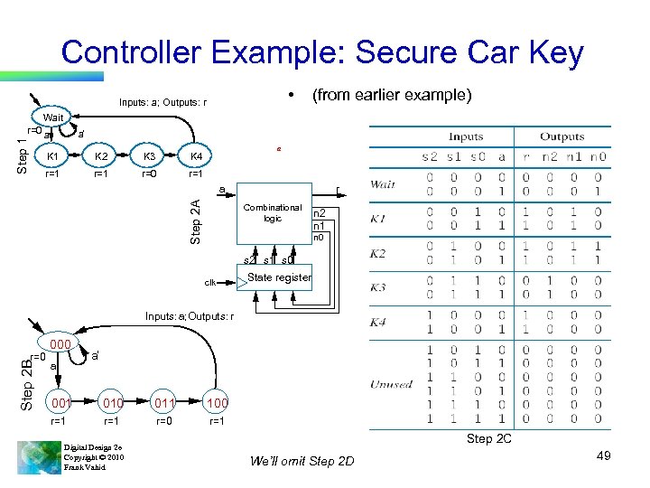 Controller Example: Secure Car Key • Inputs: a; Outputs: r Step 1 Wait r=0 a (from earlier example) a’ K 1 K 2 K 3 r=1 r=0 a K 4 r=1 Step 2 A a r Combinational logic n 2 n 1 n 0 s 2 s 1 s 0 clk State register Inputs: a; Outputs: r Step 2 B r=0 000 a a’ 001 010 011 100 r=1 r=0 r=1 Digital Design 2 e Copyright © 2010 Frank Vahid Step 2 C We’ll omit Step 2 D 49
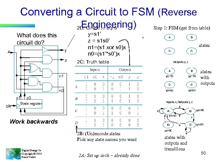 Converting a Circuit to FSM (Reverse Engineering) 2 D: Circuit to eqns What does this circuit do? y x z y=s 1’ z = s 1 s 0’ n 1=(s 1 xor s 0)x n 0=(s 1’*s 0’)x Step 1: FSM (get from table) a states 2 C: Truth table states with outputs n 1 n 0 s 1 clk s 0 State register Work backwards 2 B: (Un)encode states Pick any state names you want Digital Design 2 e Copyright © 2010 Frank Vahid 2 A: Set up arch – already done states with outputs and transitions 50
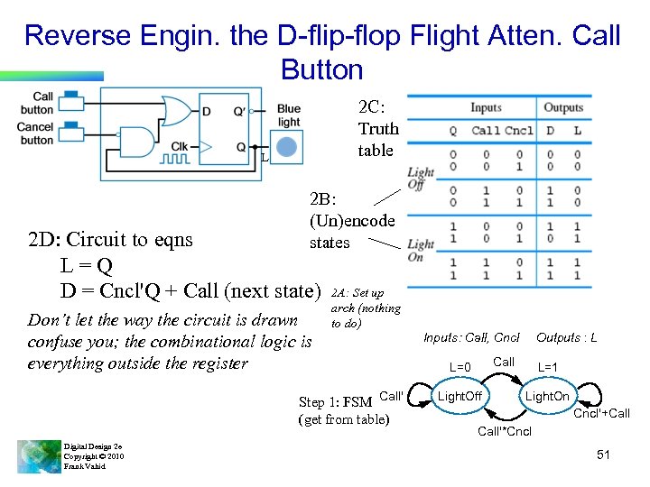 Reverse Engin. the D-flip-flop Flight Atten. Call Button 2 C: Truth table L 2 B: (Un)encode states 2 D: Circuit to eqns L=Q D = Cncl'Q + Call (next state) Don’t let the way the circuit is drawn confuse you; the combinational logic is everything outside the register 2 A: Set up arch (nothing to do) Step 1: FSM Call' (get from table) Digital Design 2 e Copyright © 2010 Frank Vahid Inputs: Call, Cncl Outputs : L Call L=0 Light. Off L=1 Light. On Cncl'+Call'*Cncl 51
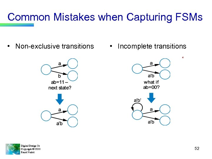 Common Mistakes when Capturing FSMs • Non-exclusive transitions • Incomplete transitions a Digital Design 2 e Copyright © 2010 Frank Vahid 52
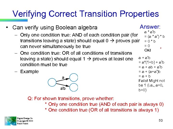 Verifying Correct Transition Properties • Can verify using Boolean algebra Answer: a * a’b = (a * a’) * b =0*b =0 a OK! – Only one condition true: AND of each condition pair (for transitions leaving a state) should equal 0 proves pair can never simultaneously be true – One condition true: OR of all conditions of transitions leaving a state) should equal 1 proves at least one a + a’b = a*(1+b) + a’b condition must be true = a + ab + a’b = a + (a+a’)b – Example =a+b Fails! Might not be 1 (i. e. , a=0, b=0) Q: For shown transitions, prove whether: * Only one condition true (AND of each pair is always 0) * One condition true (OR of all transitions is always 1) Digital Design 2 e Copyright © 2010 Frank Vahid 53
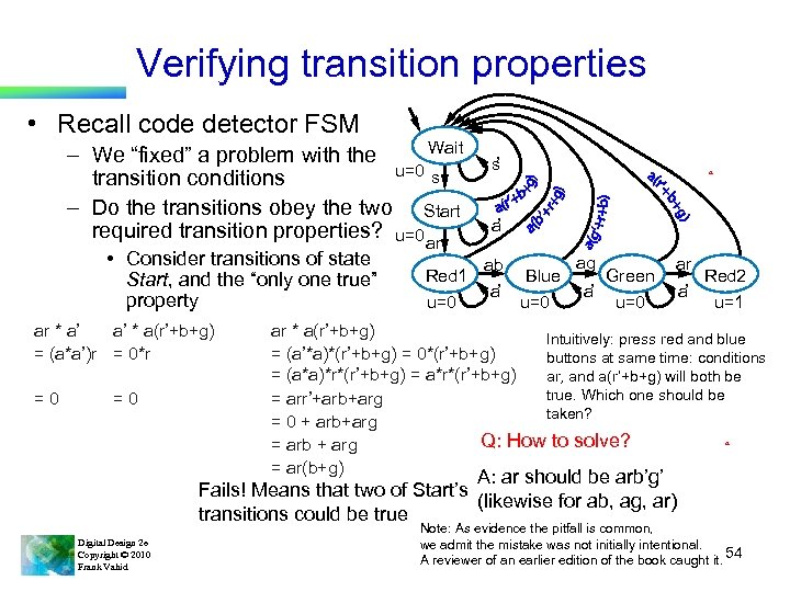 Verifying transition properties • Recall code detector FSM Wait – We “fixed” a problem with the u=0 s transition conditions – Do the transitions obey the two Start required transition properties? u=0 ar • Consider transitions of state Start, and the “only one true” property ar * a’ a’ * a(r’+b+g) = (a*a’)r = 0*r =0 =0 Red 1 u=0 s ’ a a ’ ab a ’ Blue u=0 ag a’ Green ar u=0 Red 2 u=1 ar * a(r’+b+g) Intuitively: press red and blue = (a’*a)*(r’+b+g) = 0*(r’+b+g) buttons at same time: conditions = (a*a)*r*(r’+b+g) = a*r*(r’+b+g) ar, and a(r’+b+g) will both be true. Which one should be = arr’+arb+arg taken? = 0 + arb+arg a Q: How to solve? = arb + arg = ar(b+g) A: ar should be arb’g’ Fails! Means that two of Start’s (likewise for ab, ag, ar) transitions could be true Digital Design 2 e Copyright © 2010 Frank Vahid a’ Note: As evidence the pitfall is common, we admit the mistake was not initially intentional. A reviewer of an earlier edition of the book caught it. 54
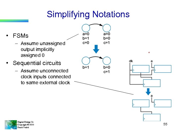 Simplifying Notations • FSMs – Assume unassigned output implicitly assigned 0 a • Sequential circuits – Assume unconnected clock inputs connected to same external clock Digital Design 2 e Copyright © 2010 Frank Vahid 55
 Mathematical Formalisms • Two formalisms to capture behavior thus far – Boolean equations for combinational circuit design – FSMs for sequential circuit design • Not necessary – But tremendously beneficial • Structured methodology • Correct circuits • Automated design, automated verification, many more advantages Digital Design 2 e Copyright © 2010 Frank Vahid 56
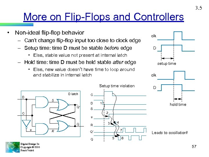 3. 5 More on Flip-Flops and Controllers • Non-ideal flip-flop behavior – Can’t change flip-flop input too close to clock edge – Setup time: time D must be stable before edge clk D • Else, stable value not present at internal latch – Hold time: time D must be held stable after edge setup time • Else, new value doesn’t have time to loop around and stabilize in internal latch clk Setup time violation D D latch D S C D Q¢ 1 hold time S 2 C u Q u R R 7 Q¢ Q Digital Design 2 e Copyright © 2010 Frank Vahid 4 3 5 Leads to oscillation! 6 57
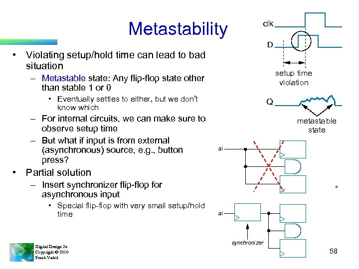 Metastability clk D • Violating setup/hold time can lead to bad situation setup time violation – Metastable state: Any flip-flop state other than stable 1 or 0 • Eventually settles to either, but we don’t know which – For internal circuits, we can make sure to observe setup time – But what if input is from external (asynchronous) source, e. g. , button press? Q metastable state ai • Partial solution – Insert synchronizer flip-flop for asynchronous input • Special flip-flop with very small setup/hold time Digital Design 2 e Copyright © 2010 Frank Vahid a ai synchronizer 58
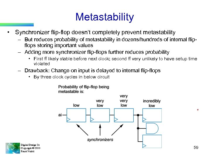 Metastability • Synchronizer flip-flop doesn’t completely prevent metastability – But reduces probability of metastability in dozens/hundreds of internal flipflops storing important values – Adding more synchronizer flip-flops further reduces probability • First ff likely stable before next clock; second ff very unlikely to have setup time violated – Drawback: Change on input is delayed to internal flip-flops • By three clock cycles in below circuit a Digital Design 2 e Copyright © 2010 Frank Vahid 59
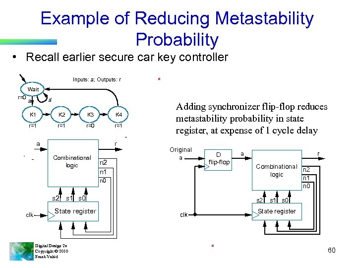 Example of Reducing Metastability Probability • Recall earlier secure car key controller Inputs: a; Outputs: r a Wait r=0 a’ a K 1 K 2 K 3 r=1 r=0 Adding synchronizer flip-flop reduces metastability probability in state register, at expense of 1 cycle delay K 4 r=1 outputs a FSM inputs r Combinational logic n 2 n 1 Original a D flip-flop n 0 s 2 s 1 s 0 clk State register Digital Design 2 e Copyright © 2010 Frank Vahid a r Combinational n 2 logic n 1 n 0 s 2 s 1 s 0 State register clk a 60
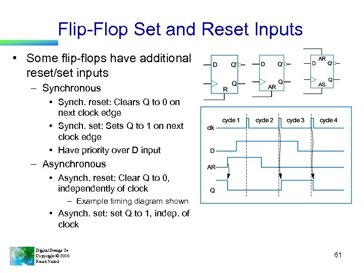 Flip-Flop Set and Reset Inputs • Some flip-flops have additional reset/set inputs – Synchronous • Synch. reset: Clears Q to 0 on next clock edge • Synch. set: Sets Q to 1 on next clock edge • Have priority over D input – Asynchronous • Asynch. reset: Clear Q to 0, independently of clock – Example timing diagram shown • Asynch. set: set Q to 1, indep. of clock Digital Design 2 e Copyright © 2010 Frank Vahid 61
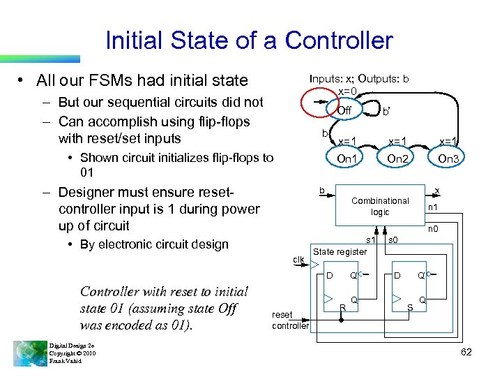 Initial State of a Controller • All our FSMs had initial state Inputs: x; Outputs: b x=0 – But our sequential circuits did not – Can accomplish using flip-flops with reset/set inputs Off b – Designer must ensure resetcontroller input is 1 during power up of circuit x=1 x=1 On 1 • Shown circuit initializes flip-flops to 01 On 2 On 3 b x Combinational logic clk s 1 State register D Digital Design 2 e Copyright © 2010 Frank Vahid n 1 n 0 • By electronic circuit design Controller with reset to initial state 01 (assuming state Off was encoded as 01). b’ reset controller Q’ R Q s 0 D Q’ S Q 62
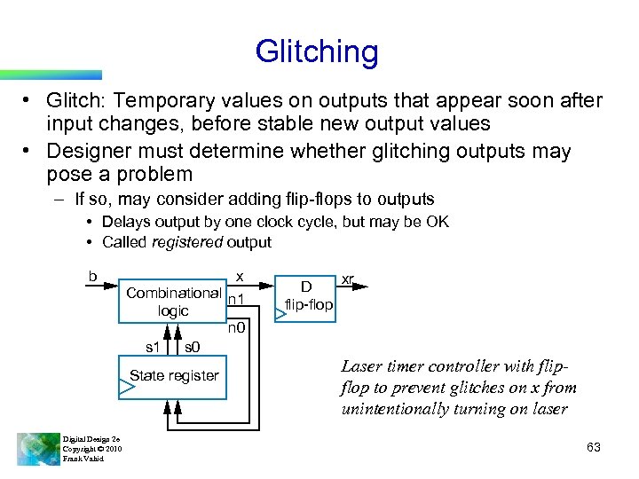 Glitching • Glitch: Temporary values on outputs that appear soon after input changes, before stable new output values • Designer must determine whether glitching outputs may pose a problem – If so, may consider adding flip-flops to outputs • Delays output by one clock cycle, but may be OK • Called registered output x b Combinational n 1 logic n 0 s 1 s 0 State register Digital Design 2 e Copyright © 2010 Frank Vahid D flip-flop xr Laser timer controller with flipflop to prevent glitches on x from unintentionally turning on laser 63
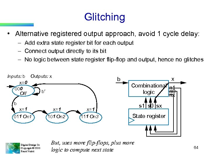 Glitching • Alternative registered output approach, avoid 1 cycle delay: – Add extra state register bit for each output – Connect output directly to its bit – No logic between state register flip-flop and output, hence no glitches Inputs: b Outputs: x x=0 000 b¢ Off x b Combinational n 1 n 0 logic nx b x=1 011 On 1 101 On 2 111 On 3 s 1 s 0 sx x=1 Digital Design 2 e Copyright © 2010 Frank Vahid State register But, uses more flip-flops, plus more logic to compute next state 64
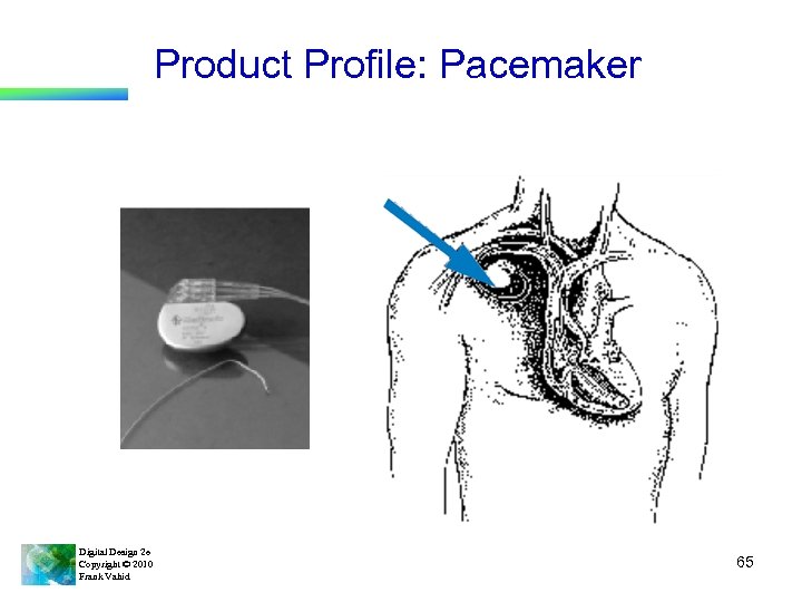 Product Profile: Pacemaker Digital Design 2 e Copyright © 2010 Frank Vahid 65
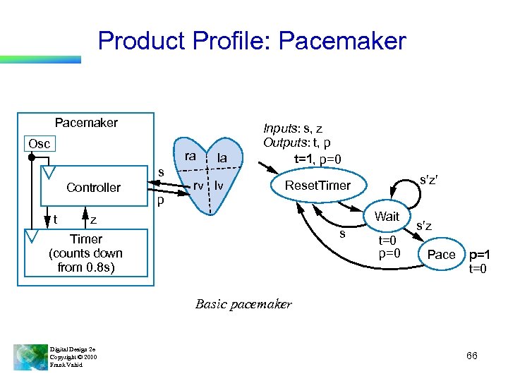 Product Profile: Pacemaker Osc ra s Controller t la rv lv Inputs: s, z Outputs: t, p t=1, p=0 s¢z¢ Reset. Timer p Wait z s Timer (counts down from 0. 8 s) t=0 p=0 s¢z Pace p=1 t=0 Basic pacemaker Digital Design 2 e Copyright © 2010 Frank Vahid 66
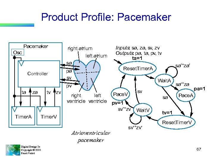 Product Profile: Pacemaker right atrium left atrium sa Osc pa sv Controller Inputs: sa, za, sv, zv Outputs: pa, ta, pv, tv ta=1 Wait. A pv ta Timer. A za tv zv Pace. V right left ventricle pv=1 sv¢*zv sv sa Wait. V Timer. V Atrioventricular pacemaker Digital Design 2 e Copyright © 2010 Frank Vahid sa¢*za¢ Reset. Timer. A sv¢*zv¢ sa¢*za pa=1 Pace. A tv=1 Reset. Timer. V 67
 Chapter Summary • Sequential circuits – Have state • Created robust bit-storage device: D flip-flop – Put several together to build register, which we used to store state • Defined FSM model to capture sequential behavior – Using mathematical models – Boolean equations for combinational circuit, and FSMs for sequential circuits – is important • Defined Capture/Convert process for sequential circuit design – Converted FSM to standard controller architecture • So now we know how to build the class of sequential circuits known as controllers Digital Design 2 e Copyright © 2010 Frank Vahid 68


