6565bdc0a471b765e322c2e79fb5a516.ppt
- Количество слайдов: 31
 Device Level Packaging of RF MEMS Mohammad Shahriar Rahman Advisor: Dr. Zeynep Çelik-Butler The Nanotechnology Research and Teaching Facility University of Texas at Arlington, TX 76019 1
 Introduction / Motivation MEMS Packaging Challenges q Most expensive process in MEMS device fabrication q Difficult due to MEMS moving structures q Application specific: hermetic or vacuum sealing q Isolation from ambient environment while exposure to agent(s) to be measured q Scalability from device to wafer level 2
 Introduction / Motivation Why MEMS Resonators? q The resonance frequency and Q-factor depends on the pressure of the vacuum cavity inside the package q Serves as a good test-bed for “growing your ownpackage” Approach q. First the package is fabricated without any resonator. q. Later resonator is integrated with the package for self packaged MEMS device. 3
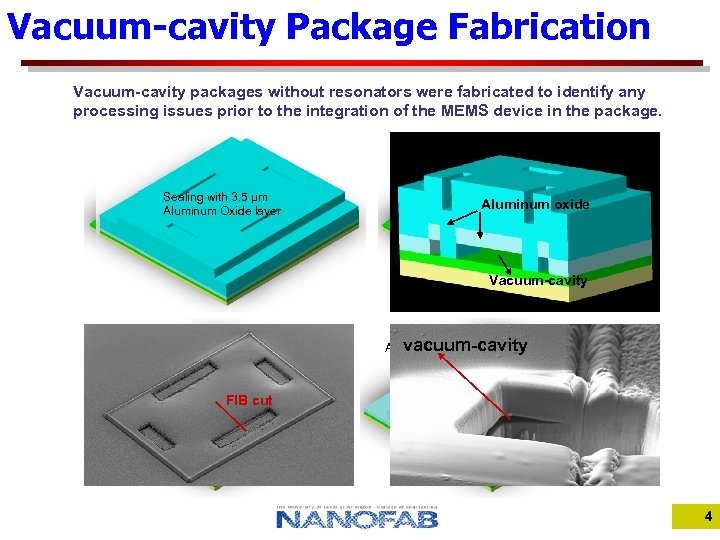 Vacuum-cavity Package Fabrication Vacuum-cavity packages without resonators were fabricated to identify any processing issues prior to the integration of the MEMS device in the package. Sealing with 3. 5 µm Aluminum Oxide layer o Silicon dioxide 6000 A Aluminum oxide PI 2737 2. 5 µm Vacuum-cavity Aluminum Oxide 0. 8 µm vacuum-cavity Ash PI 2737 Trench Cuts FIB cut 4
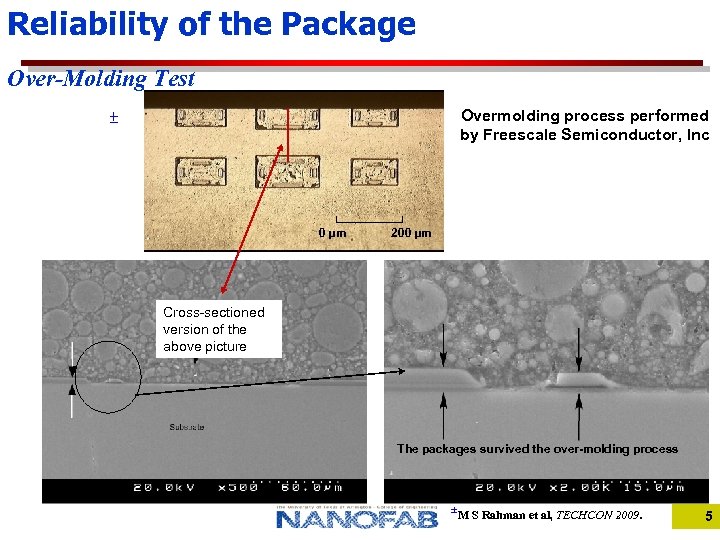 Reliability of the Package Over-Molding Test Overmolding process performed by Freescale Semiconductor, Inc ± 0 µm 200 µm Cross-sectioned version of the above picture The packages survived the over-molding process ±M S Rahman et al, TECHCON 2009. 5
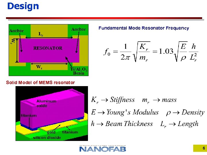 Design Anchor Lr Anchor Fundamental Mode Resonator Frequency Wr RESONATOR We Ti/Al 2 O 3 Beam Solid Model of MEMS resonator Aluminum oxide titanium gold titanium silicon dioxide 6
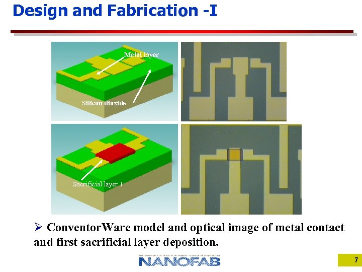 Design and Fabrication -I Metal layer Silicon dioxide Sacrificial layer 1 Ø Conventor. Ware model and optical image of metal contact and first sacrificial layer deposition. 7
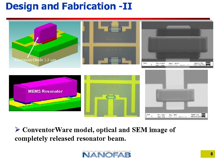 Design and Fabrication -II Aluminum Oxide 1. 3 µm MEMS Resonator Ø Conventor. Ware model, optical and SEM image of completely released resonator beam. 8
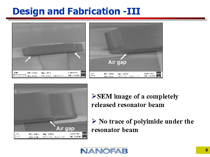 Design and Fabrication -III Air gap ØSEM image of a completely released resonator beam Air gap Ø No trace of polyimide under the resonator beam 9
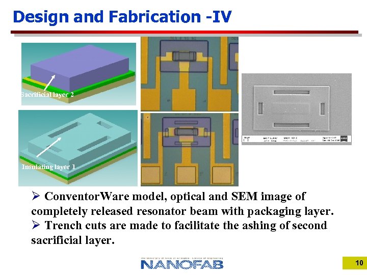 Design and Fabrication -IV Sacrificial layer 2 Insulating layer 1 Ø Conventor. Ware model, optical and SEM image of completely released resonator beam with packaging layer. Ø Trench cuts are made to facilitate the ashing of second sacrificial layer. 10
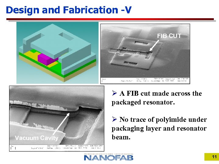 Design and Fabrication -V FIB CUT Ø A FIB cut made across the packaged resonator. Vacuum Cavity Ø No trace of polyimide under packaging layer and resonator beam. 11
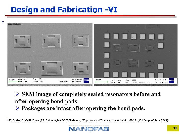 Design and Fabrication -VI ± Ø SEM image of completely sealed resonators before and after opening bond pads Ø Packages are intact after opening the bond pads. ± D. Butler, Z. Celik-Butler, M. Chitteboyina M. S. Rahman, US provisional Patent Application No. 61/218, 032 (Applied June 2009). 12
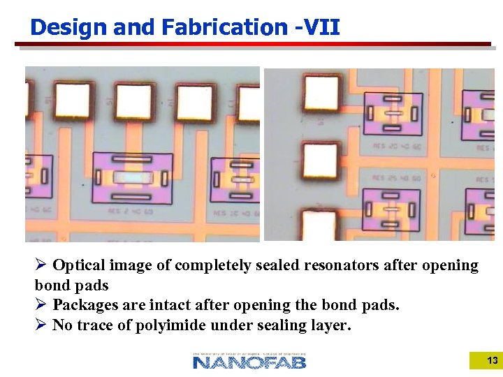 Design and Fabrication -VII Ø Optical image of completely sealed resonators after opening bond pads Ø Packages are intact after opening the bond pads. Ø No trace of polyimide under sealing layer. 13
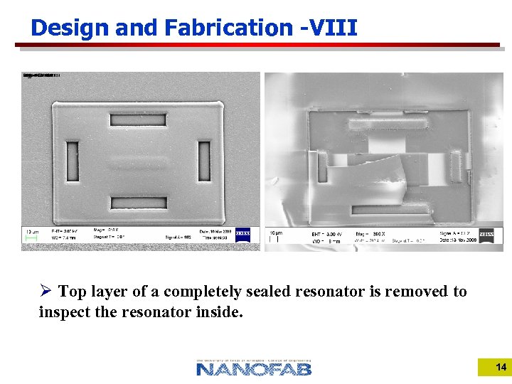 Design and Fabrication -VIII Ø Top layer of a completely sealed resonator is removed to inspect the resonator inside. 14
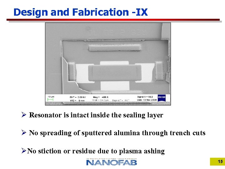 Design and Fabrication -IX Ø Resonator is intact inside the sealing layer Ø No spreading of sputtered alumina through trench cuts ØNo stiction or residue to plasma ashing 15
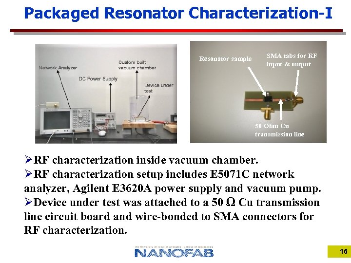 Packaged Resonator Characterization-I Resonator sample SMA tabs for RF input & output 50 Ohm Cu transmission line ØRF characterization inside vacuum chamber. ØRF characterization setup includes E 5071 C network analyzer, Agilent E 3620 A power supply and vacuum pump. ØDevice under test was attached to a 50 Ω Cu transmission line circuit board and wire-bonded to SMA connectors for RF characterization. 16
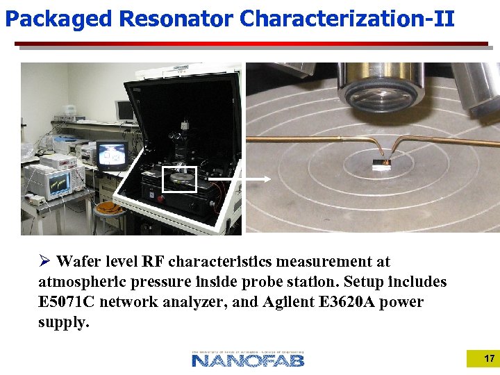 Packaged Resonator Characterization-II Ø Wafer level RF characteristics measurement at atmospheric pressure inside probe station. Setup includes E 5071 C network analyzer, and Agilent E 3620 A power supply. 17
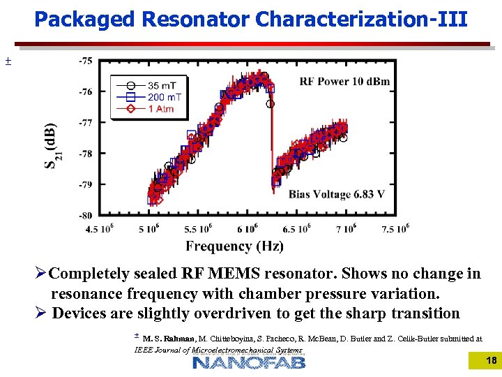 Packaged Resonator Characterization-III ± ØCompletely sealed RF MEMS resonator. Shows no change in resonance frequency with chamber pressure variation. Ø Devices are slightly overdriven to get the sharp transition ± M. S. Rahman, M. Chitteboyina, S. Pacheco, R. Mc. Bean, D. Butler and Z. Celik-Butler submitted at IEEE Journal of Microelectromechanical Systems 18
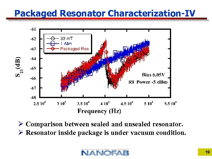 Packaged Resonator Characterization-IV Ø Comparison between sealed and unsealed resonator. Ø Resonator inside package is under vacuum condition. 19
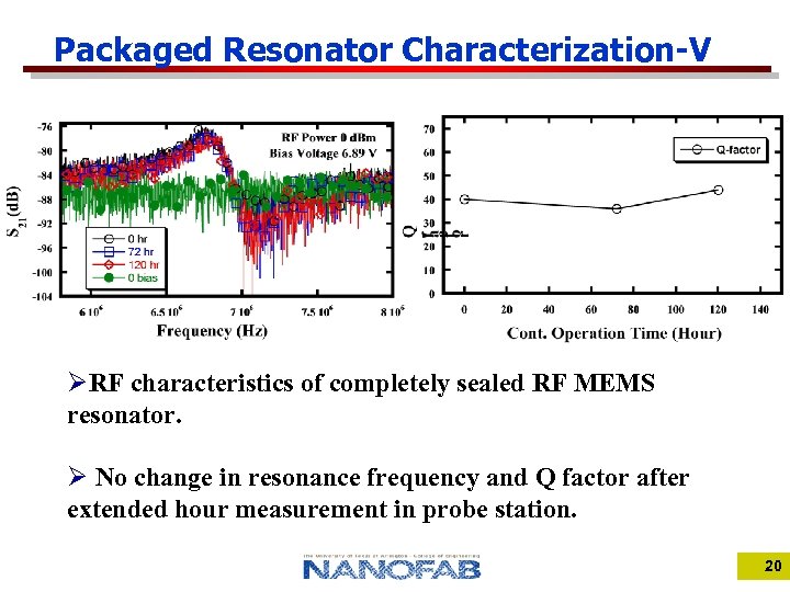 Packaged Resonator Characterization-V ØRF characteristics of completely sealed RF MEMS resonator. Ø No change in resonance frequency and Q factor after extended hour measurement in probe station. 20
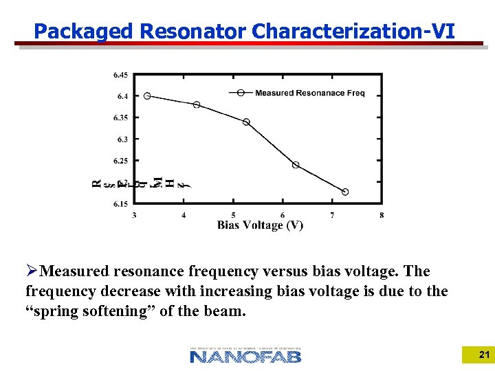 Packaged Resonator Characterization-VI ØMeasured resonance frequency versus bias voltage. The frequency decrease with increasing bias voltage is due to the “spring softening” of the beam. 21
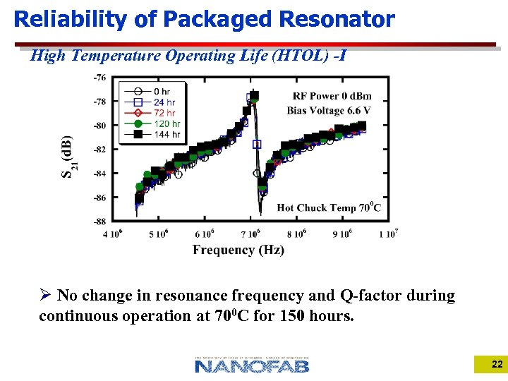 Reliability of Packaged Resonator High Temperature Operating Life (HTOL) -I Ø No change in resonance frequency and Q-factor during continuous operation at 700 C for 150 hours. 22
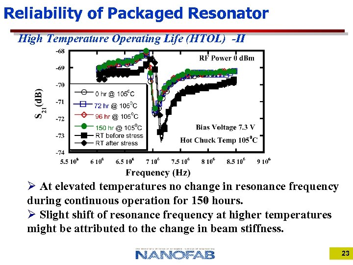 Reliability of Packaged Resonator High Temperature Operating Life (HTOL) -II Ø At elevated temperatures no change in resonance frequency during continuous operation for 150 hours. Ø Slight shift of resonance frequency at higher temperatures might be attributed to the change in beam stiffness. 23
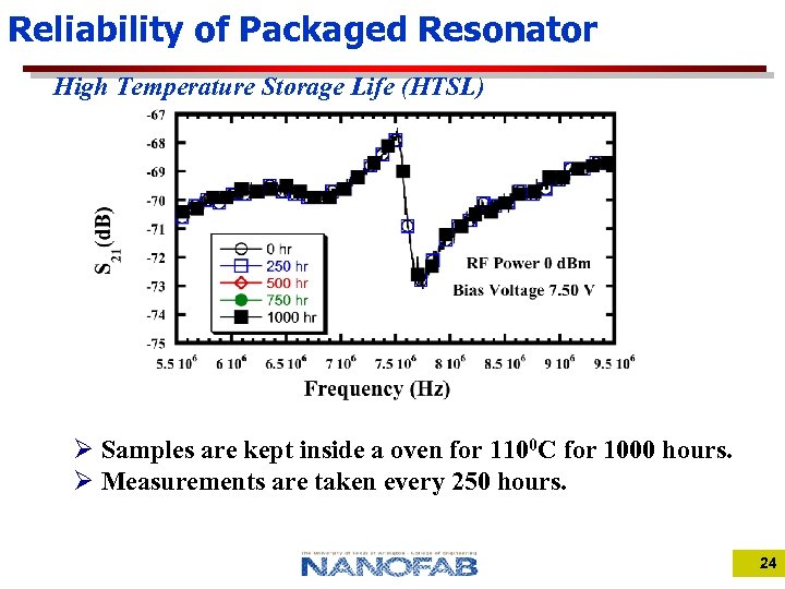 Reliability of Packaged Resonator High Temperature Storage Life (HTSL) Ø Samples are kept inside a oven for 1100 C for 1000 hours. Ø Measurements are taken every 250 hours. 24
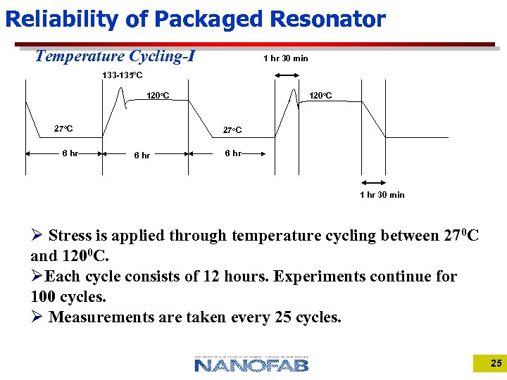 Reliability of Packaged Resonator Temperature Cycling-I 1 hr 30 min 133 -135°C 120 o. C 27 o. C 6 hr 1 hr 30 min Ø Stress is applied through temperature cycling between 270 C and 1200 C. ØEach cycle consists of 12 hours. Experiments continue for 100 cycles. Ø Measurements are taken every 25 cycles. 25
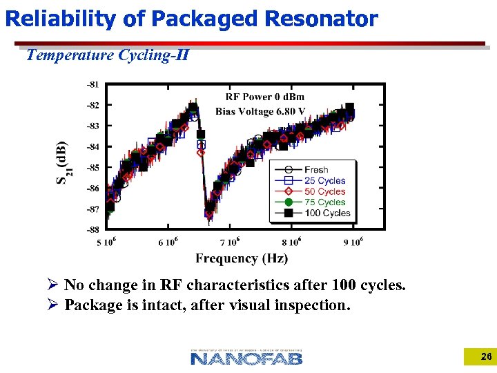 Reliability of Packaged Resonator Temperature Cycling-II Ø No change in RF characteristics after 100 cycles. Ø Package is intact, after visual inspection. 26
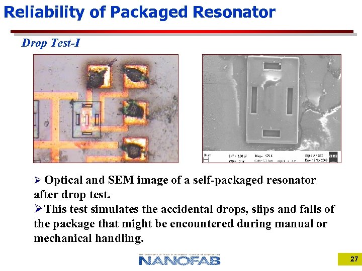 Reliability of Packaged Resonator Drop Test-I Ø Optical and SEM image of a self-packaged resonator after drop test. ØThis test simulates the accidental drops, slips and falls of the package that might be encountered during manual or mechanical handling. 27
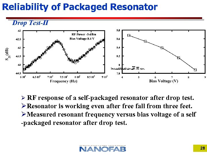 Reliability of Packaged Resonator Drop Test-II Ø RF response of a self-packaged resonator after drop test. ØResonator is working even after free fall from three feet. ØMeasured resonant frequency versus bias voltage of a self -packaged resonator after drop test. 28
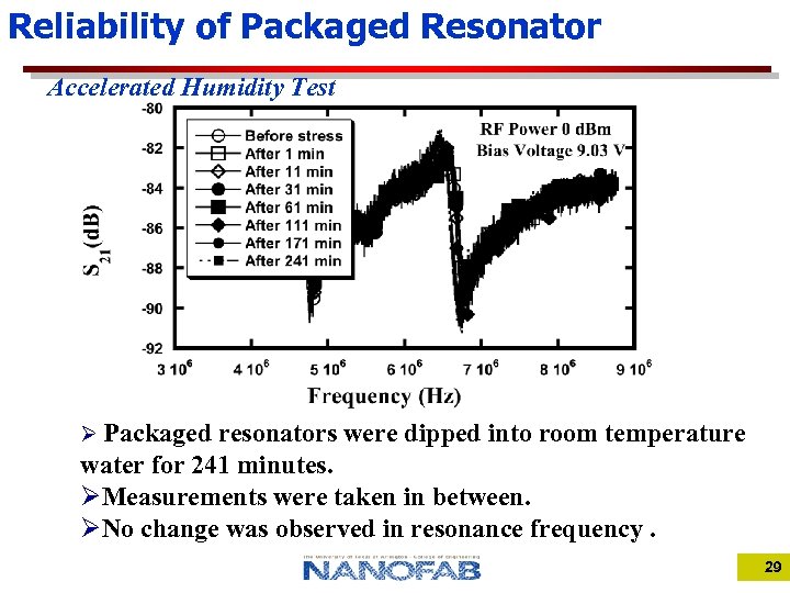 Reliability of Packaged Resonator Accelerated Humidity Test Ø Packaged resonators were dipped into room temperature water for 241 minutes. ØMeasurements were taken in between. ØNo change was observed in resonance frequency. 29
 Conclusions q CMOS process compatible MEMS self-packaging technique has been developed. q MEMS resonators have been designed, fabricated and tested. q Sealing of MEMS resonators has been successfully demonstrated based on a double-sacrificial-layer surface micromachining technique. q Resonators are successfully integrated with the developed self-packaging technique to achieve vacuum encapsulation. q Extensive characterization has been done on self-packaged MEMS resonators q Overmolding and long term and accelerated life testing of vacuum encapsulated MEMS resonators are performed. q No noticeable degradation on the package stability and device performance has been observed after long term and accelerated life testing. 30
 Acknowledgements • UTA Nano. FAB Facility • SRC- 2006 -KJ-1414 • Thanks to – Sergio Pacheco, Freescale Semiconductor – Ronald Mc. Bean, Freescale Semiconductor 31


