b599f58511463bfdddd1cfc0755aaea9.ppt
- Количество слайдов: 21
 Development of “Large gas Electron Multiplier” (LEM) detectors for high gain operation in ultra-pure noble gasses B. Baibussinov, G. Mannocchi, G. Meng, F. Pietropaolo, P. Picchi, S. Centro. R&D Experiment - INFN PD - GR. V
 Ideas and Goals (from 2006 proposal) n The basic idea: n Macroscopic version of hole Gas Electron Multipliers (GEM’s) n n n Goals: n Stable High gain (> 104 up to streamer regime) in pure noble gasses n n n quenching gas replaced by UV photon absorption in hole walls Good energy resolution n negligible charge loss due to electron diffusion and avalanche size (small wrt hole size) Direct readout of LEM electrodes n n ~mm hole size in standard double-face Cu-clad Printed Circuit Board (PCB) Characteristics & performance under investigation by several collaborations X-Y segmentation Possible applications: n Cryogenic double phase TPC’s n n High pressure TPC for medical imaging n n low energy (~ke. V) event localization (Dark Matter, Solar Neutrinos) R&D activity fully funded in PD by PRIN 2005 Photosensitive large area detectors, RICH n coupling with radiation conversion detectors (Cs. I photocathodes) 2
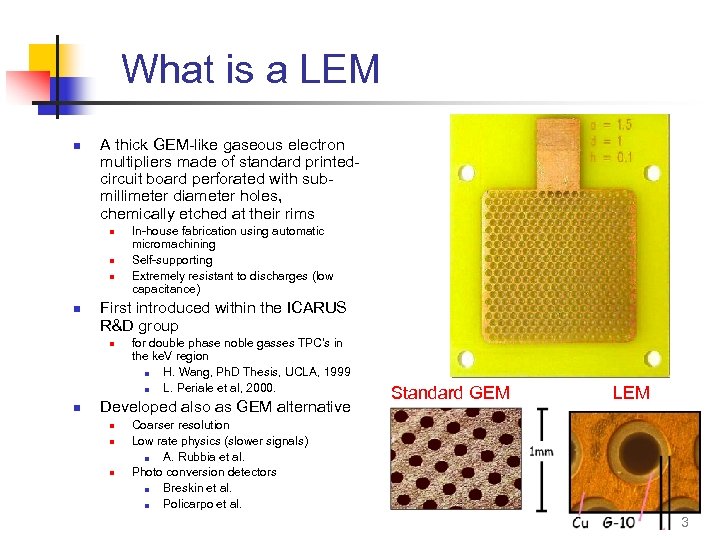 What is a LEM n A thick GEM-like gaseous electron multipliers made of standard printedcircuit board perforated with submillimeter diameter holes, chemically etched at their rims n n First introduced within the ICARUS R&D group n n In-house fabrication using automatic micromachining Self-supporting Extremely resistant to discharges (low capacitance) for double phase noble gasses TPC’s in the ke. V region n H. Wang, Ph. D Thesis, UCLA, 1999 n L. Periale et al, 2000. Developed also as GEM alternative n n n Standard GEM LEM Coarser resolution Low rate physics (slower signals) n A. Rubbia et al. Photo conversion detectors n Breskin et al. n Policarpo et al. 3
 LEM: principle of operation n Upon application of a voltage difference across the LEM, a strong dipole field Ehole is established within the holes. n n Electrons deposited by ionizing radiation in a conversion region above the LEM, or produced on a solid radiation converter, are drifting towards the LEM under Edrift and are focused into the LEM holes by a strong electric field inside the holes. Electrons are multiplied within the holes under the high electric field (~25 -50 k. V/cm) Avalanche electrons are collected on the LEM bottom electrode (a fraction could also be further transferred to a collecting anode or to a second, possibly similar, multiplier element). Each hole acts as an independent multiplier. n n A more favorable hole aspect ratio allows better avalanche confinement, reducing photon-mediated secondary effects. This leads to higher gains in LEM wrt GEM with similar gas mixtures and to high-gain operation in a large variety of gases, including highly scintillating ones like pure noble gasses or CF 4. 4
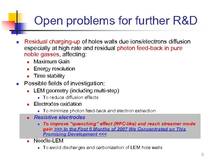 Open problems for further R&D n Residual charging-up of holes walls due ions/electrons diffusion especially at high rate and residual photon feed-back in pure noble gasses, affecting: n n Maximum Gain Energy resolution Time stability Possible fields of investigation: n LEM geometry (including multi-step) n n Electrodes oxidation n n To minimize photon feed-back and electron extraction Resistive electrodes n n To reduce diffusion effects To improve “quenching” effect (RPC-like) and reach streamer mode gain >>> In the First 6 Months of 2007 We Concentrated on This Promising Development <<< Needle-LEM n To avoid discharges and carbonization of LEM hole walls 5
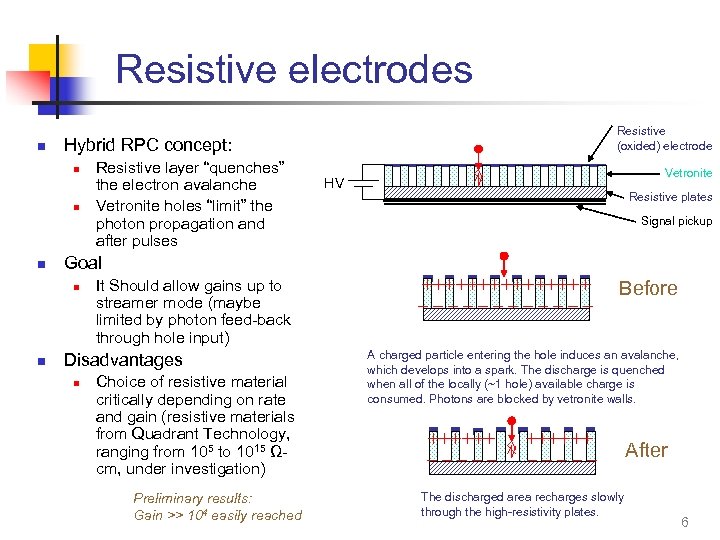 Resistive electrodes n Hybrid RPC concept: n n n Resistive layer “quenches” the electron avalanche Vetronite holes “limit” the photon propagation and after pulses Vetronite HV Resistive plates Signal pickup Goal n n Resistive (oxided) electrode It Should allow gains up to streamer mode (maybe limited by photon feed-back through hole input) Disadvantages n Choice of resistive material critically depending on rate and gain (resistive materials from Quadrant Technology, ranging from 105 to 1015 Ωcm, under investigation) Preliminary results: Gain >> 104 easily reached ++++++++ ______ Before A charged particle entering the hole induces an avalanche, which develops into a spark. The discharge is quenched when all of the locally (~1 hole) available charge is consumed. Photons are blocked by vetronite walls. ++++++ _____ The discharged area recharges slowly through the high-resistivity plates. After 6
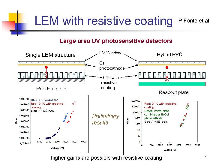 LEM with resistive coating P. Fonte et al. Large area UV photosensitive detectors Single LEM structure UV Window Hybrid RPC Cs. I photocathode Readout plate G-10 with resistive coating Blue: Cu coated G-10 Red: G-10 with resistive coating. Gas: Ar+5% isob. Preliminary results Readout plate Red: G-10 with resistive coating. Green: same plate combined with Cs. I photocathode. Gas : Ar+5% isob. higher gains are possible with resistive coating 7
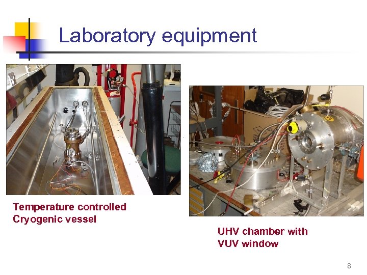 Laboratory equipment Temperature controlled Cryogenic vessel UHV chamber with VUV window 8
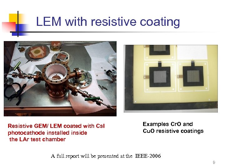 LEM with resistive coating Resistive GEM/ LEM coated with Cs. I photocathode installed inside the LAr test chamber Examples Cr. O and Cu. O resistive coatings A full report will be presented at the IEEE-2006 9
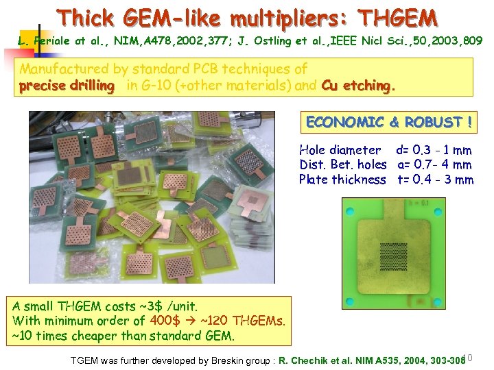 Thick GEM-like multipliers: THGEM L. Periale at al. , NIM, A 478, 2002, 377; J. Ostling et al. , IEEE Nicl Sci. , 50, 2003, 809 Manufactured by standard PCB techniques of precise drilling in G-10 (+other materials) and Cu etching ECONOMIC & ROBUST ! Hole diameter d= 0. 3 - 1 mm Dist. Bet. holes a= 0. 7 - 4 mm Plate thickness t= 0. 4 - 3 mm A small THGEM costs ~3$ /unit. With minimum order of 400$ ~120 THGEMs. ~10 times cheaper than standard GEM. 10 TGEM was further developed by Breskin group : R. Chechik et al. NIM A 535, 2004, 303 -308
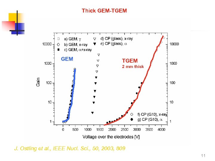 Thick GEM-TGEM 2 mm thick J. Ostling et al. , IEEE Nucl. Sci. , 50, 2003, 809 11
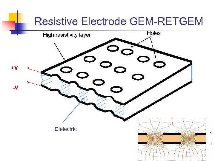 Resistive Electrode GEM-RETGEM High resistivity layer Holes +V -V Dielectric + 12
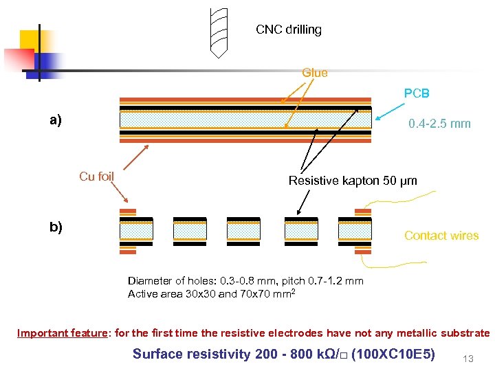 CNC drilling Glue PCB a) 0. 4 -2. 5 mm Cu foil Resistive kapton 50 μm b) Contact wires Diameter of holes: 0. 3 -0. 8 mm, pitch 0. 7 -1. 2 mm Active area 30 x 30 and 70 x 70 mm 2 Important feature: for the first time the resistive electrodes have not any metallic substrate Surface resistivity 200 - 800 kΩ/□ (100 XC 10 E 5) 13
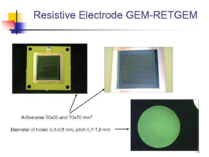 Resistive Electrode GEM-RETGEM Active area 30 x 30 and 70 x 70 mm 2 Diameter of holes: 0. 3 -0. 8 mm, pitch 0. 7 -1. 2 mm 14
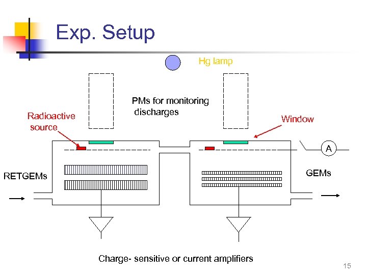 Exp. Setup Hg lamp Radioactive source PMs for monitoring discharges Window A GEMs RETGEMs Charge- sensitive or current amplifiers 15
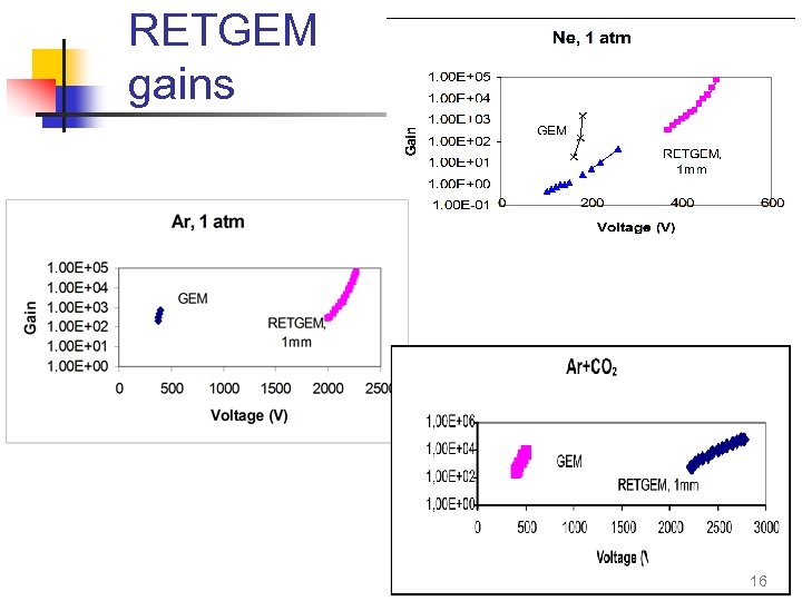 RETGEM gains 16
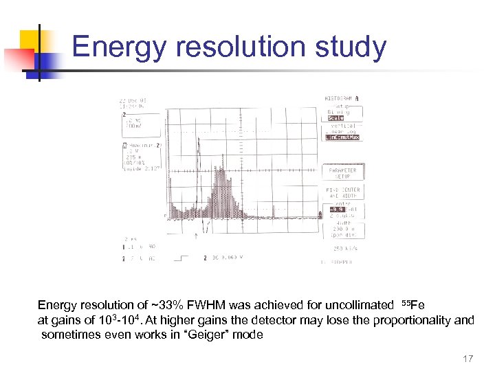 Energy resolution study Energy resolution of ~33% FWHM was achieved for uncollimated 55 Fe at gains of 103 -104. At higher gains the detector may lose the proportionality and sometimes even works in “Geiger” mode 17
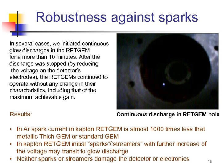 Robustness against sparks In several cases, we initiated continuous glow discharges in the RETGEM for a more than 10 minutes. After the discharge was stopped (by reducing the voltage on the detector’s electrodes), the RETGEMs continued to operate without any change in their characteristics, including that of the maximum achievable gain. Results: Continuous discharge in RETGEM hole • In Ar spark current in kapton RETGEM is almost 1000 times less that metallic Thich GEM or standard GEM • In kapton RETGEM initial “sparks”/’streamers” with further increase of the voltage may transit to glow discharge • Neither sparks or streamers damage the detector or electronics 18
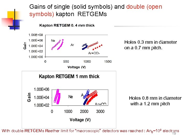 Gains of single (solid symbols) and double (open symbols) kapton RETGEMs Holes 0. 3 mm in diameter on a 0. 7 mm pitch. Holes 0. 8 mm in diameter with a 1. 2 mm pitch With double RETGEMs Raether limit for “macroscopic” detectors was reached : An 0~108 electrons 19
 Recent preprints and publications n n n n R. Oliveira, V. Peskov, F. Pietropaolo and P. Picchi, First tests of thick GEMs with electrodes made of a resistive kapton, NIM-A 576, (June 2007) Pages 362 -366 L. Periale, V. Peskov, C. Iacobaeus, B. Lund-Jensen, P. Picchi, F. Pietropaolo and I. Rodionov, Photosensitive gaseous detectors for cryogenic temperature applications, NIM-A 573, (April 2007) Pages 302 -305 L. Periale, V. Peskov, A. Braem, Di Mauro, P. Martinengo, P. Picchi, F. Pietropaolo and H. Sipila, Development of new sealed UV sensitive gaseous detectors and their applications, NIM-A 572, (March 2007), Pages 189 -192 L. Periale, V. Peskov, C. Iacobaeus, B. Lund-Jensen, P. Pavlopoulos, P. Picchi and F. Pietropaolo, A study of the operation of especially designed photosensitive gaseous detectors at cryogenic temperatures, NIM-A 567, (November 2006) Pages 381 -385 A. Di Mauro et al. , Development of innovative micropattern gaseous detectors with resistive electrodes and first results of their applications, ar. Xiv: 0706. 0102; 04 Jun 2007 V. Peskov, R. de Oliveira, F. Pietropaolo, P. Picchi, First Tests of Thick GEMs with Electrodes Made of a Resistive Kapton, ar. Xiv: physics/0701154; 13 Jan 2007 Di Mauro, A, Lund-Jensen, B. , Martinengo, P. , Nappi, E. , Peskov, V. Periale, L. , Picchi, P. ; Pietropaolo, F. ; Rodionov, I. , A New GEM-like Imaging Detector with Electrodes Coated with Resistive Layers, ar. Xiv: physics/0612166; 17 Dec 2006, Nuclear Science Symposium Conference record 2006, IEEE Volume 6, (Oct. 2006) Page(s): 3852 - 3859 V. Peskov, B. Baibussinov, S. Centro, A. Di Mauro, B. Lund-Jensen, P. Martinengo, E. Nappi, R. de Oliveira, F. Pietropaolo, P. Picchi, L. Periale, I. Rodionov, S. Ventura, Development and first tests of GEM-like Detectors with Resistive Electrodes, Nuclear Science, IEEE Accepted for publication (July 2007) 20
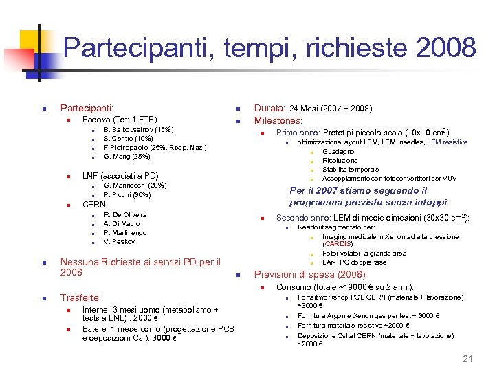 Partecipanti, tempi, richieste 2008 n Partecipanti: n Padova (Tot: 1 FTE) n n n G. Mannocchi (20%) P. Picchi (30%) R. De Oliveira A. Di Mauro P. Martinengo V. Peskov Nessuna Richieste ai servizi PD per il 2008 Trasferte: n n Interne: 3 mesi uomo (metabolismo + tests a LNL) : 2000 € Estere: 1 mese uomo (progettazione PCB e deposizioni Cs. I): 3000 € ottimizzazione layout LEM, LEM+needles, LEM resistive n Guadagno n Risoluzione n Stabilita temporale n Accoppiamento con fotoconvertitori per VUV Per il 2007 stiamo seguendo il programma previsto senza intoppi n Secondo anno: LEM di medie dimesioni (30 x 30 cm 2): n n Readout segmentato per: n Imaging medicale in Xenon ad alta pressione (CARDIS) n Fotorivelatori a grande area n LAr-TPC doppia fase Previsioni di spesa (2008): n n Primo anno: Prototipi piccola scala (10 x 10 cm 2): CERN n n n B. Baiboussinov (15%) S. Centro (10%) F. Pietropaolo (25%, Resp. Naz. ) G. Meng (25%) Durata: 24 Mesi (2007 + 2008) Milestones: LNF (associati a PD) n n n Consumo (totale ~19000 € su 2 anni): n n Forfait workshop PCB CERN (materiale + lavorazione) ~3000 € Fornitura Argon e Xenon gas per test ~ 3000 € Fornitura materiale resistivo ~2000 € Deposizione Cs. I al CERN (materiale + lavorazione) ~2000 € 21


