2f069c6fa140c7d4d47b2315c0b8caa8.ppt
- Количество слайдов: 22
Design Considerations and Improvement by Using Chip and Package Co-Simulation Yeong-Jar Chang, Meng-Xin Jiang, Chen-Wei Chang, Wang. Jin Chen, Faraday Technology Corporation, Taiwan, R. O. C. Charlie Shih, Jack Lin Cadence Design Systems 1
Overview • Traditional Package Design Consideration • Proposed Flow • Per-pin Inductance Checking and Improvement • Coupling Checking and Improvement • Co-simulation and Improvement 2
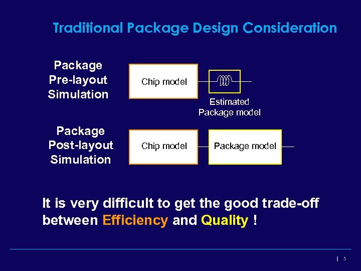
Traditional Package Design Consideration Package Pre-layout Simulation Chip model Package Post-layout Simulation Chip model Estimated Package model It is very difficult to get the good trade-off between Efficiency and Quality ! 3
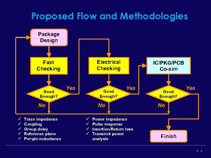
Proposed Flow and Methodologies Package Design Electrical Checking Fast Checking Good Enough? Yes Good Enough? Trace impedance Coupling Group delay Reference plane Per-pin inductance Yes No No ü ü ü IC/PKG/PCB Co-sim ü ü Power impedance Pulse response Insertion/Return loss Transient power analysis Good Enough? Yes No Finish 4
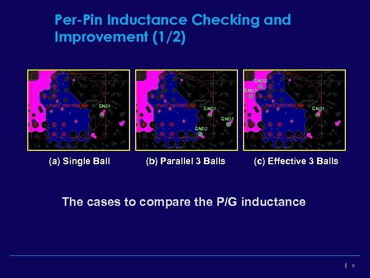
Per-Pin Inductance Checking and Improvement (1/2) GND 2 GND 3 GND 1 GND 3 GND 2 (a) Single Ball (b) Parallel 3 Balls (c) Effective 3 Balls The cases to compare the P/G inductance 5
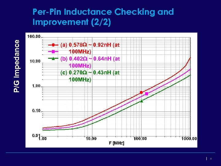
P/G Impedance Per-Pin Inductance Checking and Improvement (2/2) (a) 0. 578 W ~ 0. 92 n. H (at 100 MHz) (b) 0. 402 W ~ 0. 64 n. H (at 100 MHz) (c) 0. 270 W ~ 0. 43 n. H (at 100 MHz) 6
Design Consideration (1) • Do not treat via, lead-frame or BGA ball as simple inductors only • Parallel scheme can not always get the reduction as we expected • The better position, case (c), can achieve 33% improvement than case (b) with the same number of ground balls 7
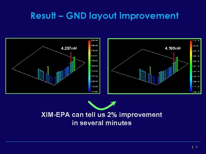
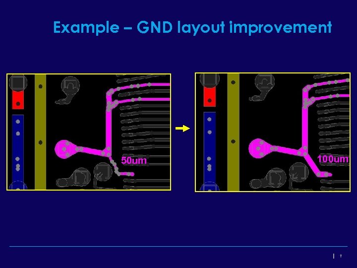
Result – GND layout improvement 4. 267 n. H 4. 195 n. H XIM-EPA can tell us 2% improvement in several minutes 8
Example – GND layout improvement 50 um 100 um 9
Coupling Behavior - Even Mode and Odd Mode Odd Even 10
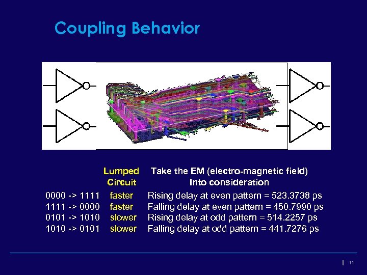
Coupling Behavior 0000 -> 1111 -> 0000 0101 -> 1010 -> 0101 Lumped Circuit faster slower Take the EM (electro-magnetic field) Into consideration Rising delay at even pattern = 523. 3738 ps Falling delay at even pattern = 450. 7990 ps Rising delay at odd pattern = 514. 2257 ps Falling delay at odd pattern = 441. 7276 ps 11
Design Consideration (2) • The coupling behavior is much different from what we think in the RC-based circuit analysis. • The corner (fast/slow) simulation will be different • We need to take the EM into consideration if the size is large or the speed is fast. For the rule of thumb, the critical size is /20. ( = wave length = speed of light / frequency ) 12
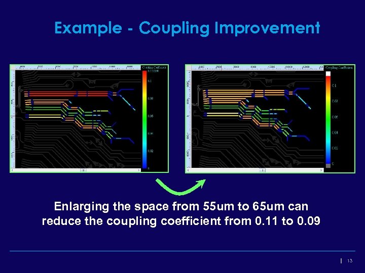
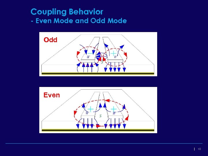
Example - Coupling Improvement Enlarging the space from 55 um to 65 um can reduce the coupling coefficient from 0. 11 to 0. 09 13
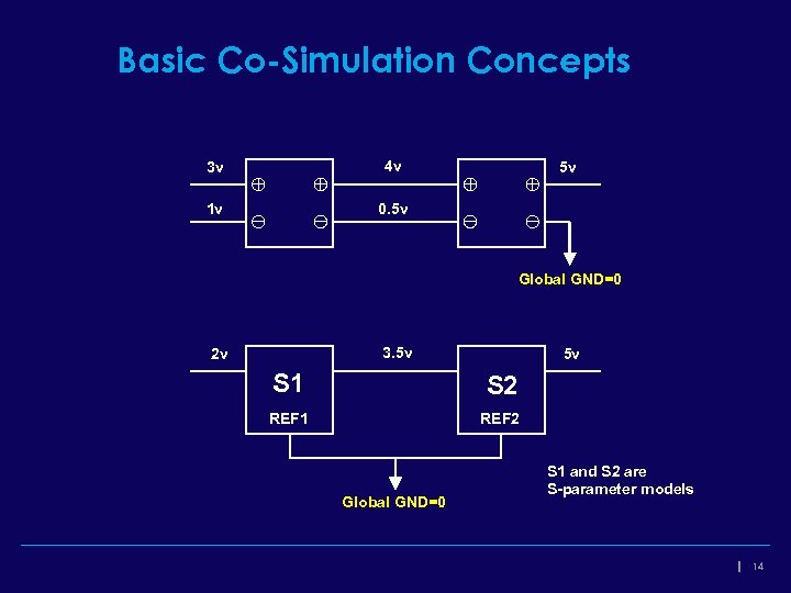
Basic Co-Simulation Concepts 3 v 4 v 1 v 0. 5 v 5 v Global GND=0 3. 5 v 2 v 5 v S 1 S 2 REF 1 REF 2 Global GND=0 S 1 and S 2 are S-parameter models 14
Design Consideration (3) • The S-parameter model is a mathematic model which records the relative voltage instead of the absolute voltage. • Connecting the REFs of S-parameters and the global GND (0 or ideal GND) together is correct for co-simulation. But, it does not mean that they are all 0 voltage. • Chip-package co-simulation is very important to know the real behavior. 15
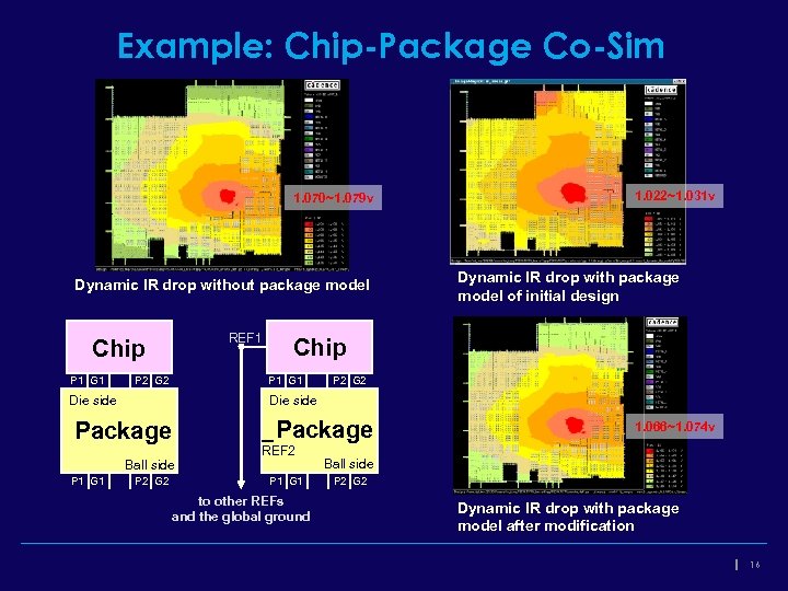
Example: Chip-Package Co-Sim 1. 070~1. 079 v Dynamic IR drop without package model REF 1 Chip P 1 G 1 P 2 G 2 Die side Package Ball side P 1 G 1 Dynamic IR drop with package model of initial design Chip P 1 G 1 Die side 1. 022~1. 031 v P 2 G 2 REF 2 P 1 G 1 to other REFs and the global ground 1. 066~1. 074 v Ball side P 2 G 2 Dynamic IR drop with package model after modification 16
Summary l Have proposed a new flow to improve the efficiency and quality of package design l The chip-level and package-level design concepts are totally different l Have introduced some design considerations for improving package design l Have consolidated the ground connections for chip-package co-simulation 17

Appendix 18
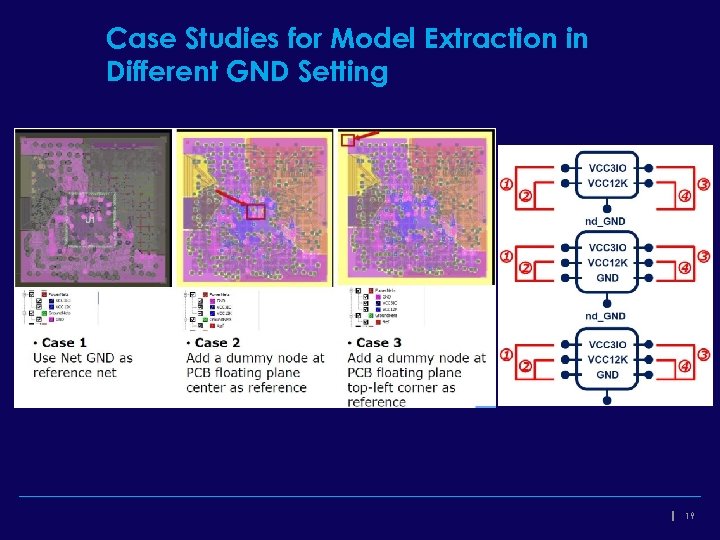
Case Studies for Model Extraction in Different GND Setting 19
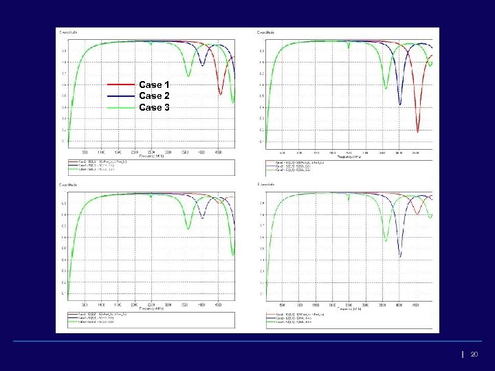
Case 1 Case 2 Case 3 20
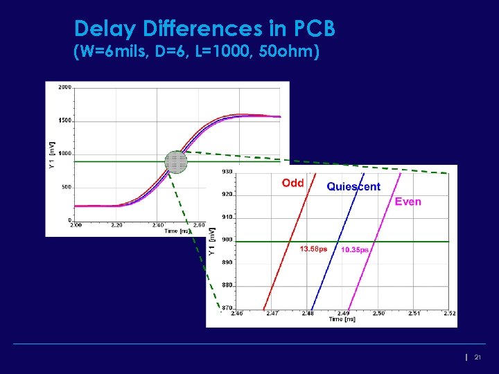
Delay Differences in PCB (W=6 mils, D=6, L=1000, 50 ohm) 21
![References [1] R. Pomerleau, S. Scearce, T. Whipple, “Using Codesign to Optimize System Interconnect References [1] R. Pomerleau, S. Scearce, T. Whipple, “Using Codesign to Optimize System Interconnect](https://present5.com/presentation/2f069c6fa140c7d4d47b2315c0b8caa8/image-22.jpg)
References [1] R. Pomerleau, S. Scearce, T. Whipple, “Using Codesign to Optimize System Interconnect Paths”, Design. Con 2011 [2] Keith Felton, “Methodology and Flow Challenges in System-level Co-design of Multi-die Packaged Systems”, Article on www. chipdesignmag. com [3] Joel Mc. Grath, "The Need for Package-Aware Methodology for IC Design" Article on www. chipdesignmag. com [4] M. Patil, et al, "Chip-package-board co-design for Complex System-on- Chip(So. C)", in Proc. EPEPS, pp. 273 -276, 2010. 22
2f069c6fa140c7d4d47b2315c0b8caa8.ppt