46c16d2378222cd8de314f45668e7ff4.ppt
- Количество слайдов: 30
D 0 Run 2 B Silicon Electronics Andrei Nomerotski, Fermilab December 3 rd 2001, Technical Design Review • • Goals SVX 4 chip Overview of Run 2 B readout Analog flex cable Hybrids Interfacing to Run 2 A readout Performance issues Summary Andrei Nomerotski, Fermilab D 0 Run 2 B Silicon Electronics
Goals • Robust system based on – new SVX 4 chip – Run 2 A readout • Minimize time, effort and cost – – Minimum R&D Recycle Run 2 A readout as much as possible Conservative, low risk solutions Simple production, testing and commissioning • Use Run 2 A commissioning experience Andrei Nomerotski, Fermilab D 0 Run 2 B Silicon Electronics
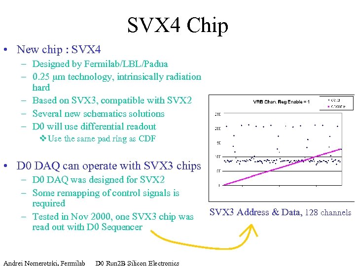
SVX 4 Chip • New chip : SVX 4 – Designed by Fermilab/LBL/Padua – 0. 25 mm technology, intrinsically radiation hard – Based on SVX 3, compatible with SVX 2 – Several new schematics solutions – D 0 will use differential readout v Use the same pad ring as CDF • D 0 DAQ can operate with SVX 3 chips – D 0 DAQ was designed for SVX 2 – Some remapping of control signals is required – Tested in Nov 2000, one SVX 3 chip was read out with D 0 Sequencer Andrei Nomerotski, Fermilab D 0 Run 2 B Silicon Electronics SVX 3 Address & Data, 128 channels
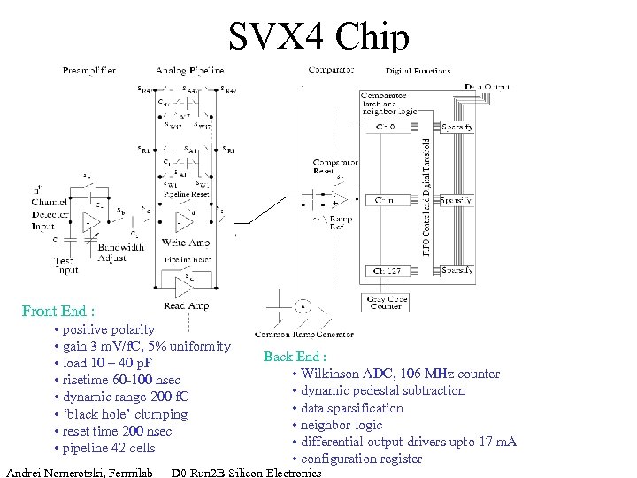
SVX 4 Chip Front End : • positive polarity • gain 3 m. V/f. C, 5% uniformity • load 10 – 40 p. F • risetime 60 -100 nsec • dynamic range 200 f. C • ‘black hole’ clumping • reset time 200 nsec • pipeline 42 cells Back End : • Wilkinson ADC, 106 MHz counter • dynamic pedestal subtraction • data sparsification • neighbor logic • differential output drivers upto 17 m. A • configuration register Andrei Nomerotski, Fermilab D 0 Run 2 B Silicon Electronics
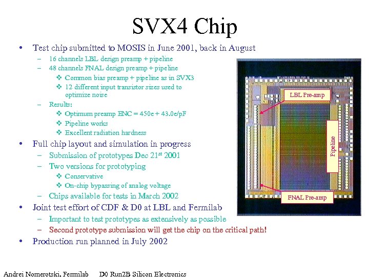
SVX 4 Chip Test chip submitted to MOSIS in June 2001, back in August – – – • 16 channels LBL design preamp + pipeline 48 channels FNAL design preamp + pipeline v Common bias preamp + pipeline as in SVX 3 v 12 different input transistor sizes used to optimize noise Results: v Optimum preamp ENC = 450 e + 43. 0 e/p. F v Pipeline works v Excellent radiation hardness LBL Pre-amp Pipeline • Full chip layout and simulation in progress – Submission of prototypes Dec 21 st 2001 – Two versions for prototyping v Conservative v On-chip bypassing of analog voltage – Chips available for tests in March 2002 • Joint test effort of CDF & D 0 at LBL and Fermilab – Important to test prototypes as extensively as possible – Second prototype submission will get the chip on the critical path! • Production run planned in July 2002 Andrei Nomerotski, Fermilab D 0 Run 2 B Silicon Electronics FNAL Pre-amp
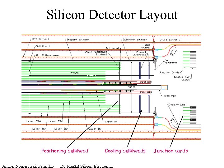
Silicon Detector Layout Positioning bulkhead Cooling bulkheads Andrei Nomerotski, Fermilab D 0 Run 2 B Silicon Electronics Junction cards
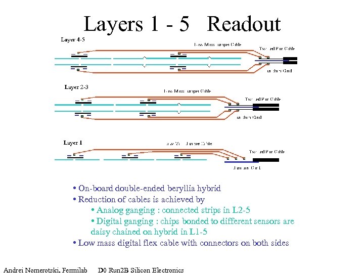
Layers 1 - 5 Readout • On-board double-ended beryllia hybrid • Reduction of cables is achieved by • Analog ganging : connected strips in L 2 -5 • Digital ganging : chips bonded to different sensors are daisy chained on hybrid in L 1 -5 • Low mass digital flex cable with connectors on both sides Andrei Nomerotski, Fermilab D 0 Run 2 B Silicon Electronics
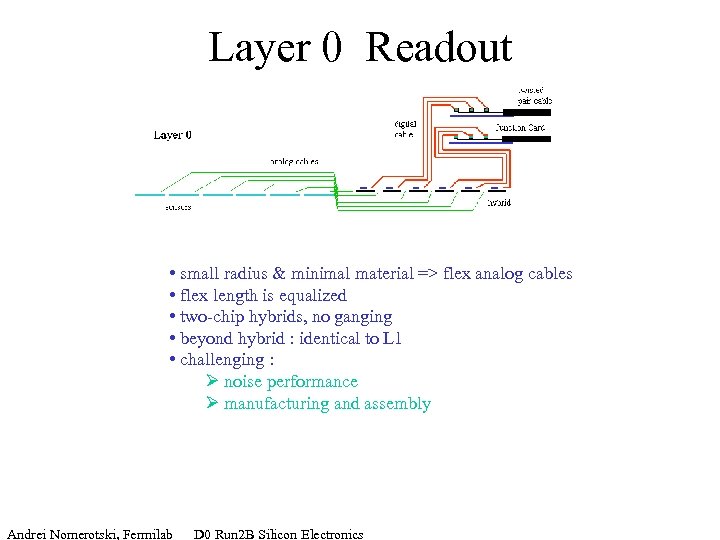
Layer 0 Readout • small radius & minimal material => flex analog cables • flex length is equalized • two-chip hybrids, no ganging • beyond hybrid : identical to L 1 • challenging : Ø noise performance Ø manufacturing and assembly Andrei Nomerotski, Fermilab D 0 Run 2 B Silicon Electronics
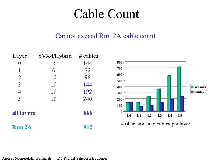
Cable Count Cannot exceed Run 2 A cable count Layer SVX 4/Hybrid # cables 0 2 144 1 6 72 2 10 96 3 10 144 4 10 192 5 10 240 all layers 888 Run 2 A 912 Andrei Nomerotski, Fermilab D 0 Run 2 B Silicon Electronics # of sensors and cables per layer
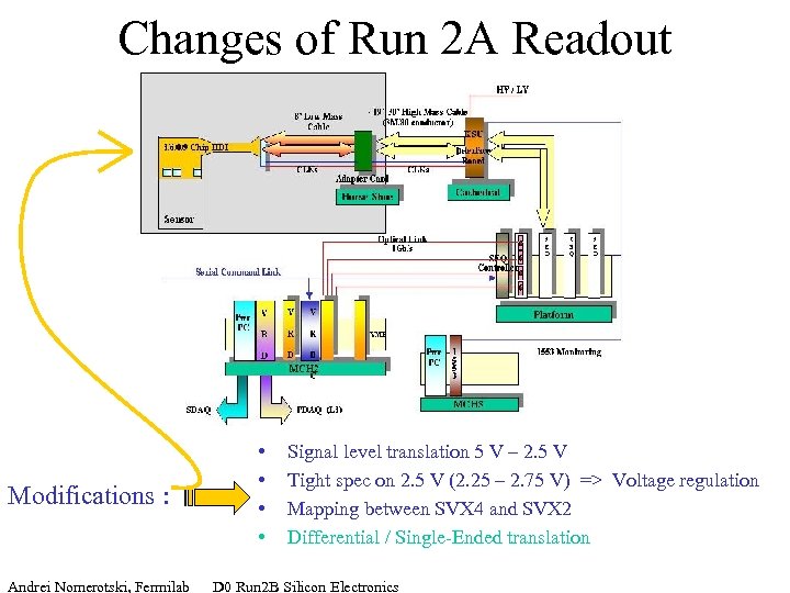
Changes of Run 2 A Readout Modifications : • • Signal level translation 5 V – 2. 5 V Tight spec on 2. 5 V (2. 25 – 2. 75 V) => Voltage regulation Mapping between SVX 4 and SVX 2 Differential / Single-Ended translation Andrei Nomerotski, Fermilab D 0 Run 2 B Silicon Electronics
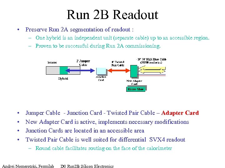
Run 2 B Readout • Preserve Run 2 A segmentation of readout : – One hybrid is an independent unit (separate cable) up to an accessible region. – Proven to be successful during Run 2 A commissioning. • • Jumper Cable - Junction Card - Twisted Pair Cable – Adapter Card New Adapter Card is active, implements necessary modifications Junction Cards are located in an accessible area Twisted Pair Cable is well suited for differential SVX 4 readout – Round cable facilitates routing on the face of the calorimeter Andrei Nomerotski, Fermilab D 0 Run 2 B Silicon Electronics
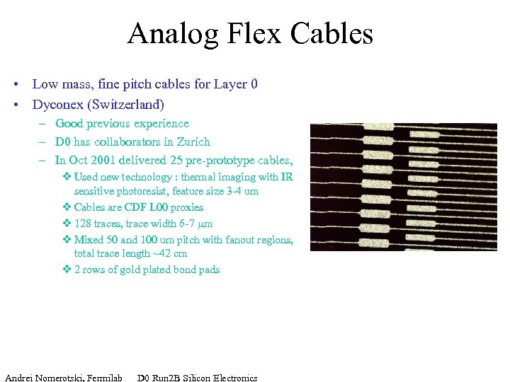
Analog Flex Cables • Low mass, fine pitch cables for Layer 0 • Dyconex (Switzerland) – Good previous experience – D 0 has collaborators in Zurich – In Oct 2001 delivered 25 pre-prototype cables, v Used new technology : thermal imaging with IR sensitive photoresist, feature size 3 -4 um v Cables are CDF L 00 proxies v 128 traces, trace width 6 -7 mm v Mixed 50 and 100 um pitch with fanout regions, total trace length ~42 cm v 2 rows of gold plated bond pads Andrei Nomerotski, Fermilab D 0 Run 2 B Silicon Electronics
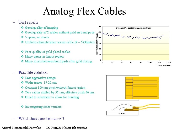
Analog Flex Cables – Test results v v Good quality of imaging Good quality of 2 cables without gold on bond pads 3 opens, no shorts Uniform characteristics across cable, R ~ 5 Ohm/cm v Poor quality of gold plated cables v Many opens in fanout region v Many shorts between bond pads after gold plating – Possible solution v v v Less aggressive design Wider traces 15 -20 um Constant 100 um pitch without fanout region Two cables shifted by 50 um, effective pitch 50 um Glued to substrates to allow for bonding v Investigating other vendors – What about performance ? Andrei Nomerotski, Fermilab D 0 Run 2 B Silicon Electronics
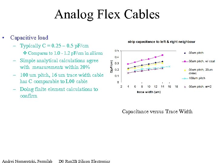
Analog Flex Cables • Capacitive load – Typically C = 0. 25 – 0. 5 p. F/cm v Compares to 1. 0 - 1. 2 p. F/cm in silicon – Simple analytical calculations agree with measurements within 20% – 100 um pitch, 16 um trace width cable has C comparable to L 00 cable – Doing finite element calculations to confirm Capacitance versus Trace Width Andrei Nomerotski, Fermilab D 0 Run 2 B Silicon Electronics
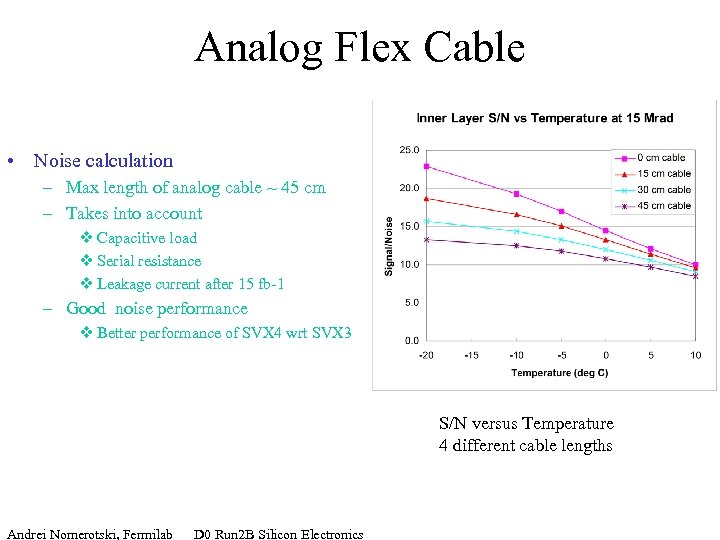
Analog Flex Cable • Noise calculation – Max length of analog cable ~ 45 cm – Takes into account v Capacitive load v Serial resistance v Leakage current after 15 fb-1 – Good noise performance v Better performance of SVX 4 wrt SVX 3 S/N versus Temperature 4 different cable lengths Andrei Nomerotski, Fermilab D 0 Run 2 B Silicon Electronics
Hybrids • Based on Beryllia ceramic, ~0. 4 mm thick – Minimize material – Good heat conductor – Established technique, possible vendor CPT, Oceanside CA • Multilayer structure on the substrate – six Au layers v GND & power planes, 4 um thick v Traces, 8 um thick, 100 um wide – five 40 um dielectric layers – Two technologies for vias in dielectric v Etching (Fodel dielectric), min via size 4 mils v Screen printing, min via size 8 mils – Screen printing is our baseline v Cost effective v More vendors available Andrei Nomerotski, Fermilab D 0 Run 2 B Silicon Electronics
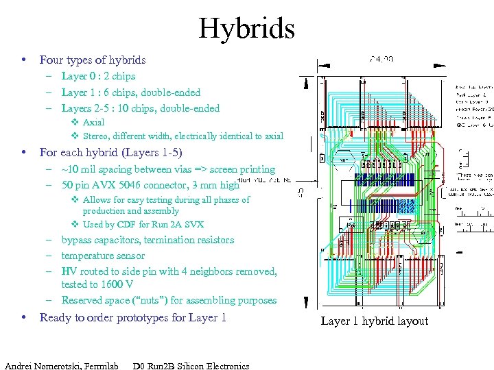
Hybrids • Four types of hybrids – Layer 0 : 2 chips – Layer 1 : 6 chips, double-ended – Layers 2 -5 : 10 chips, double-ended v Axial v Stereo, different width, electrically identical to axial • For each hybrid (Layers 1 -5) – ~10 mil spacing between vias => screen printing – 50 pin AVX 5046 connector, 3 mm high v Allows for easy testing during all phases of production and assembly v Used by CDF for Run 2 A SVX – bypass capacitors, termination resistors – temperature sensor – HV routed to side pin with 4 neighbors removed, tested to 1600 V – Reserved space (“nuts”) for assembling purposes • Ready to order prototypes for Layer 1 Andrei Nomerotski, Fermilab D 0 Run 2 B Silicon Electronics Layer 1 hybrid layout
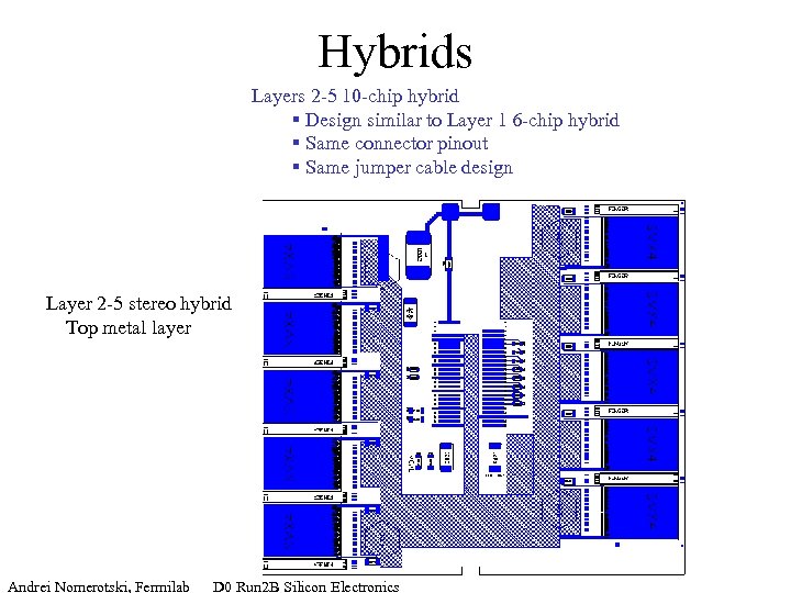
Hybrids Layers 2 -5 10 -chip hybrid § Design similar to Layer 1 6 -chip hybrid § Same connector pinout § Same jumper cable design Layer 2 -5 stereo hybrid Top metal layer Andrei Nomerotski, Fermilab D 0 Run 2 B Silicon Electronics
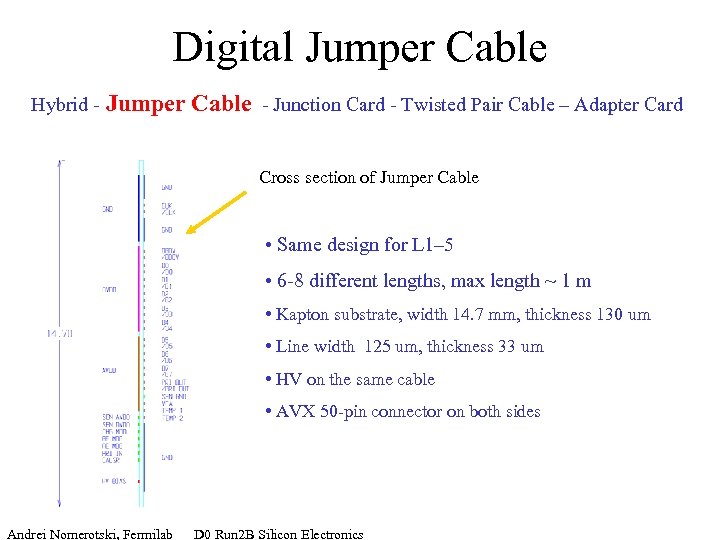
Digital Jumper Cable Hybrid - Jumper Cable - Junction Card - Twisted Pair Cable – Adapter Card Cross section of Jumper Cable • Same design for L 1– 5 • 6 -8 different lengths, max length ~ 1 m • Kapton substrate, width 14. 7 mm, thickness 130 um • Line width 125 um, thickness 33 um • HV on the same cable • AVX 50 -pin connector on both sides Andrei Nomerotski, Fermilab D 0 Run 2 B Silicon Electronics
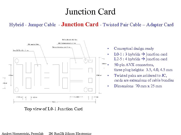
Junction Card Hybrid - Jumper Cable - Junction Card - Twisted Pair Cable – Adapter Card • • • Top view of L 0 -1 Junction Card Andrei Nomerotski, Fermilab D 0 Run 2 B Silicon Electronics Conceptual design ready L 0 -1 : 3 hybrids junction card L 2 -5 : 4 hybrids junction card 50 -pin AVX connectors, three plug heights: 3. 5, 4. 0, 4. 5 mm Twisted pairs are soldered to JC, cards are extensions of cable bundles Dimensions 70 mm x 25 mm
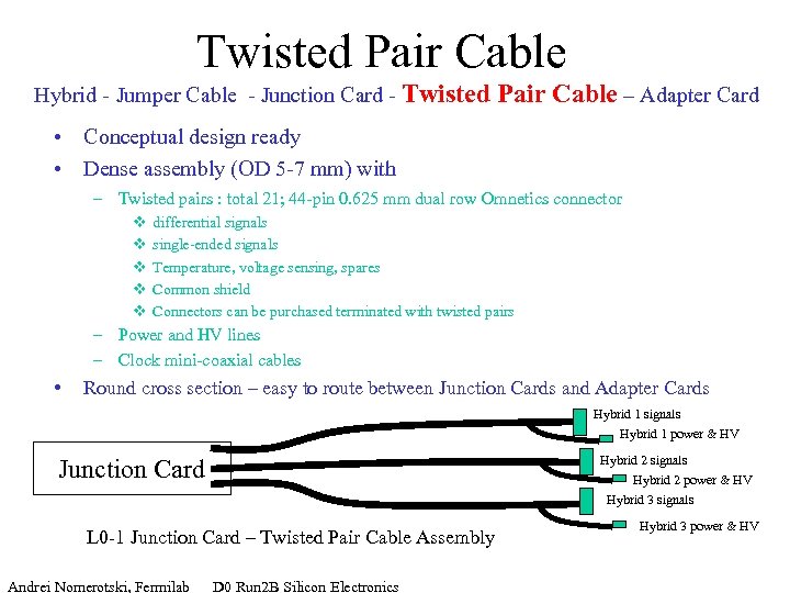
Twisted Pair Cable Hybrid - Jumper Cable - Junction Card - Twisted Pair Cable – Adapter Card • Conceptual design ready • Dense assembly (OD 5 -7 mm) with – Twisted pairs : total 21; 44 -pin 0. 625 mm dual row Omnetics connector v v v differential signals single-ended signals Temperature, voltage sensing, spares Common shield Connectors can be purchased terminated with twisted pairs – Power and HV lines – Clock mini-coaxial cables • Round cross section – easy to route between Junction Cards and Adapter Cards Hybrid 1 signals Hybrid 1 power & HV Junction Card L 0 -1 Junction Card – Twisted Pair Cable Assembly Andrei Nomerotski, Fermilab D 0 Run 2 B Silicon Electronics Hybrid 2 signals Hybrid 2 power & HV Hybrid 3 signals Hybrid 3 power & HV
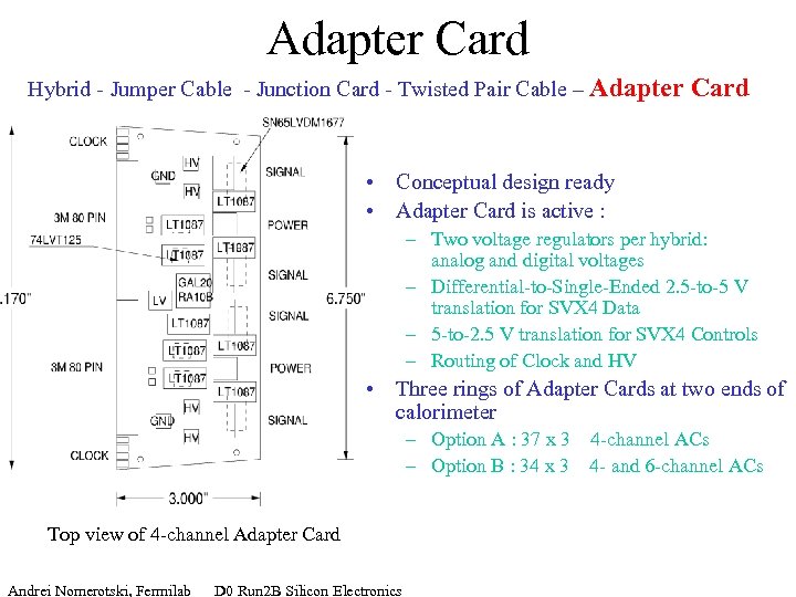
Adapter Card Hybrid - Jumper Cable - Junction Card - Twisted Pair Cable – Adapter Card • Conceptual design ready • Adapter Card is active : – Two voltage regulators per hybrid: analog and digital voltages – Differential-to-Single-Ended 2. 5 -to-5 V translation for SVX 4 Data – 5 -to-2. 5 V translation for SVX 4 Controls – Routing of Clock and HV • Three rings of Adapter Cards at two ends of calorimeter – Option A : 37 x 3 4 -channel ACs – Option B : 34 x 3 4 - and 6 -channel ACs Top view of 4 -channel Adapter Card Andrei Nomerotski, Fermilab D 0 Run 2 B Silicon Electronics
Interface Board & Power Supplies • Baseline : retain Run 2 A IB’s, use in full functionality – – – • Signal regeneration and termination LV distribution LV voltage/current monitoring HV distribution for L 2 -5 (< 300 V) Hybrid Enable/Disable Hybrid temperature monitoring Present IB fixes several SVX 2 “features” – Assumption : SVX 4 will not have new “features” which cannot be recovered with present IB – Otherwise will need new IB • Move LV power supplies to Platform – Allows for maintenance during short Controlled Accesses to Collision Hall – Replace bulk supplies with smaller ~ 7 A supplies – Voltage regulators at Adapter Card make increased length of the path acceptable Andrei Nomerotski, Fermilab D 0 Run 2 B Silicon Electronics
High Voltage • To keep up with radiation damage – Increased depletion voltage – Current few m. A / sensor v strong function of temperature – 1000 V spec for L 0 -1 – 300 V spec for L 2 -5 • One HV channel per hybrid – will have up to 4 sensors per HV channel in L 4 -5, 2 sensors in L 1 – Splitting of channels possible in outer layers • Two options : – Keep present Bi. Ra system v Meets the specifications v Must split for outer layers – Buy a new system (ex. CAEN) • Need redesign HV distribution path from Counting House to Collision Hall Andrei Nomerotski, Fermilab D 0 Run 2 B Silicon Electronics
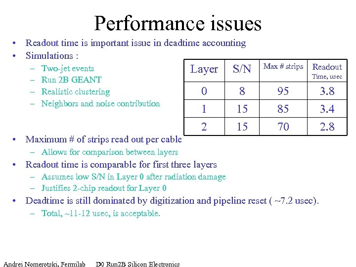
Performance issues • Readout time is important issue in deadtime accounting • Simulations : – – Two-jet events Run 2 B GEANT Realistic clustering Neighbors and noise contribution Layer S/N Max # strips 0 1 2 8 15 15 95 85 70 Readout Time, usec 3. 8 3. 4 2. 8 • Maximum # of strips read out per cable – Allows for comparison between layers • Readout time is comparable for first three layers – Assumes low S/N in Layer 0 after radiation damage – Justifies 2 -chip readout for Layer 0 • Deadtime is still dominated by digitization and pipeline reset ( ~7. 2 usec). – Total, ~11 -12 usec, is acceptable. Andrei Nomerotski, Fermilab D 0 Run 2 B Silicon Electronics
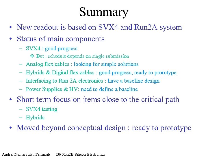
Summary • New readout is based on SVX 4 and Run 2 A system • Status of main components – SVX 4 : good progress v But : schedule depends on single submission – – Analog flex cables : looking for simple solutions Hybrids & Digital flex cables : good progress, ready to prototype Interfacing to Run 2 A electronics : have a baseline design Power Supplies & HV: need to define a baseline • Short term focus on items close to the critical path – SVX 4 testing – Hybrids • Moved beyond conceptual design : ready to prototype Andrei Nomerotski, Fermilab D 0 Run 2 B Silicon Electronics
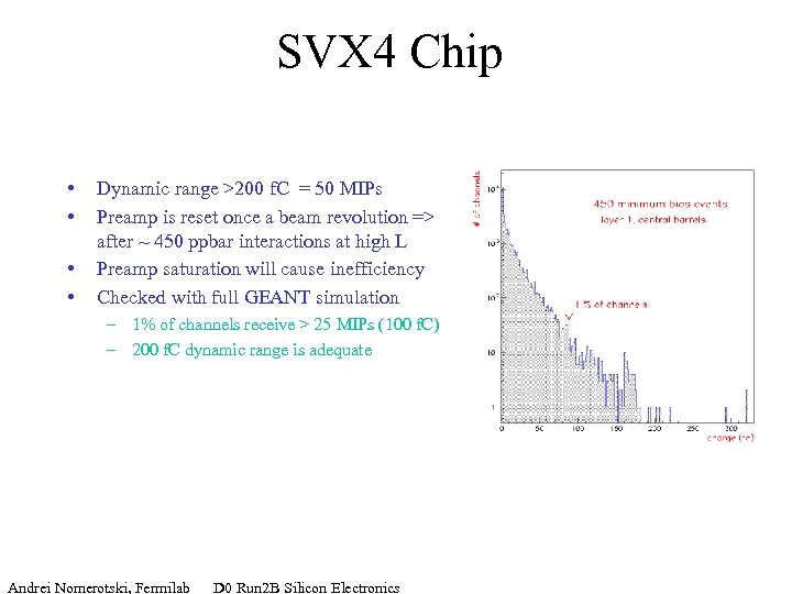
SVX 4 Chip • • Dynamic range >200 f. C = 50 MIPs Preamp is reset once a beam revolution => after ~ 450 ppbar interactions at high L Preamp saturation will cause inefficiency Checked with full GEANT simulation – 1% of channels receive > 25 MIPs (100 f. C) – 200 f. C dynamic range is adequate Andrei Nomerotski, Fermilab D 0 Run 2 B Silicon Electronics
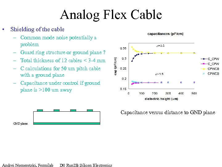
Analog Flex Cable • Shielding of the cable – Common mode noise potentially a problem – Guard ring structure or ground plane ? – Total thickness of 12 cables < 3 -4 mm – C calculations for 50 um pitch cable with a ground plane – Capacitance under control if ground plane is >100 um away Capacitance versus distance to GND plane Andrei Nomerotski, Fermilab D 0 Run 2 B Silicon Electronics
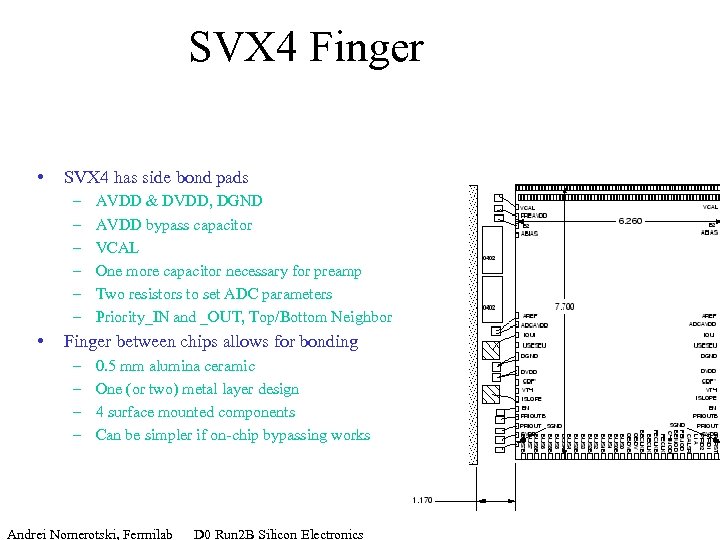
SVX 4 Finger • SVX 4 has side bond pads – – – • AVDD & DVDD, DGND AVDD bypass capacitor VCAL One more capacitor necessary for preamp Two resistors to set ADC parameters Priority_IN and _OUT, Top/Bottom Neighbor Finger between chips allows for bonding – – 0. 5 mm alumina ceramic One (or two) metal layer design 4 surface mounted components Can be simpler if on-chip bypassing works Andrei Nomerotski, Fermilab D 0 Run 2 B Silicon Electronics
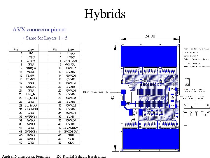
Hybrids AVX connector pinout • Same for Layers 1 – 5 Andrei Nomerotski, Fermilab D 0 Run 2 B Silicon Electronics
46c16d2378222cd8de314f45668e7ff4.ppt