33a614ca543a56bb413e8241a5f4dc86.ppt
- Количество слайдов: 37
 CS 252 Graduate Computer Architecture Lecture 5 Memory Technology February 5, 2001 Phil Buonadonna 2/5/02 CS 252/Culler Lec 5. 1
 Main Memory Background • Random Access Memory (vs. Serial Access Memory) • Different flavors at different levels – Physical Makeup (CMOS, DRAM) – Low Level Architectures (FPM, EDO, BEDO, SDRAM) • Cache uses SRAM: Static Random Access Memory – No refresh (6 transistors/bit vs. 1 transistor Size: DRAM/SRAM 4 -8, Cost/Cycle time: SRAM/DRAM 8 -16 • Main Memory is DRAM: Dynamic Random Access Memory – Dynamic since needs to be refreshed periodically (8 ms, 1% time) – Addresses divided into 2 halves (Memory as a 2 D matrix): » RAS or Row Access Strobe » CAS or Column Access Strobe 2/5/02 CS 252/Culler Lec 5. 2
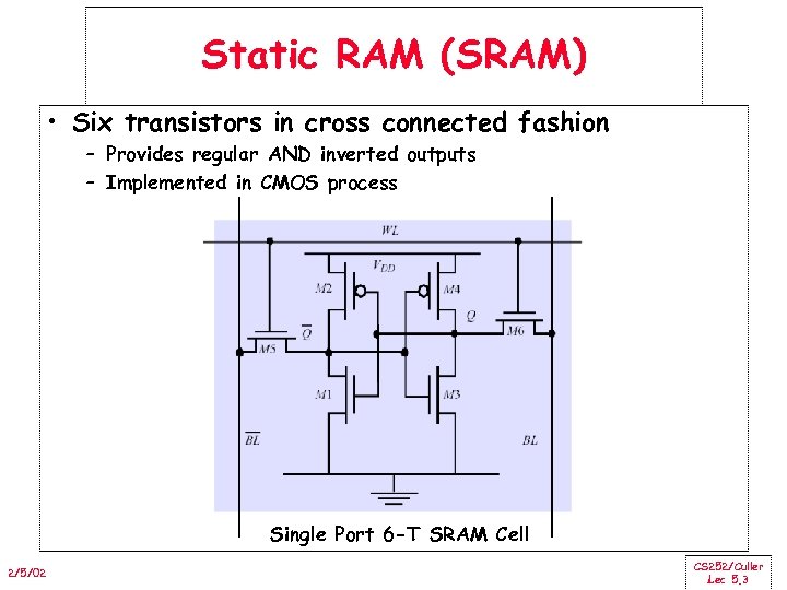 Static RAM (SRAM) • Six transistors in cross connected fashion – Provides regular AND inverted outputs – Implemented in CMOS process Single Port 6 -T SRAM Cell 2/5/02 CS 252/Culler Lec 5. 3
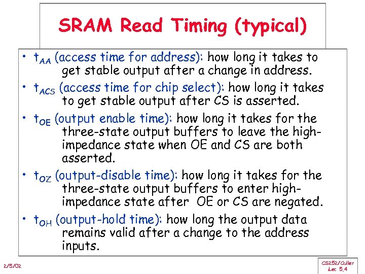 SRAM Read Timing (typical) • t. AA (access time for address): how long it takes to get stable output after a change in address. • t. ACS (access time for chip select): how long it takes to get stable output after CS is asserted. • t. OE (output enable time): how long it takes for the three-state output buffers to leave the highimpedance state when OE and CS are both asserted. • t. OZ (output-disable time): how long it takes for the three-state output buffers to enter highimpedance state after OE or CS are negated. • t. OH (output-hold time): how long the output data remains valid after a change to the address inputs. 2/5/02 CS 252/Culler Lec 5. 4
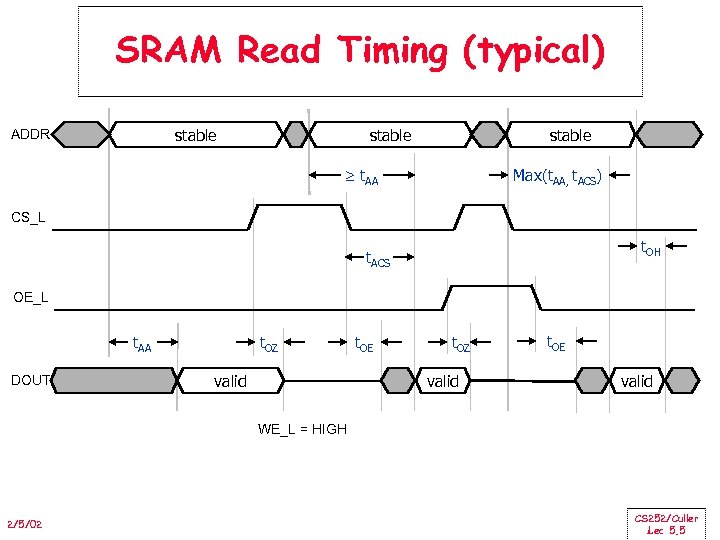 SRAM Read Timing (typical) stable ADDR stable t. AA Max(t. AA, t. ACS) CS_L t. OH t. ACS OE_L t. AA DOUT t. OZ t. OE t. OZ valid t. OE valid WE_L = HIGH 2/5/02 CS 252/Culler Lec 5. 5
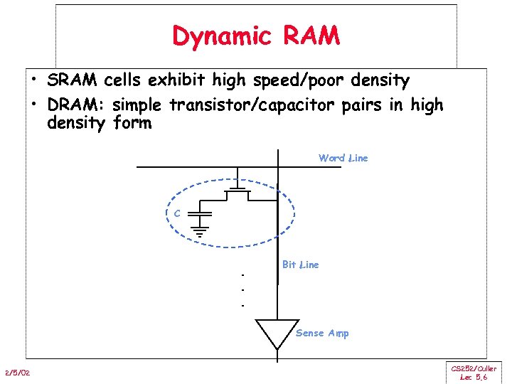 Dynamic RAM • SRAM cells exhibit high speed/poor density • DRAM: simple transistor/capacitor pairs in high density form Word Line C . . . Bit Line Sense Amp 2/5/02 CS 252/Culler Lec 5. 6
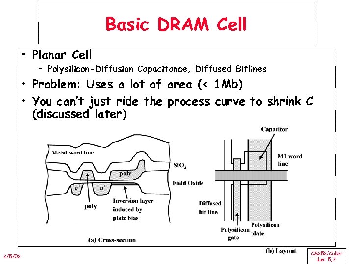 Basic DRAM Cell • Planar Cell – Polysilicon-Diffusion Capacitance, Diffused Bitlines • Problem: Uses a lot of area (< 1 Mb) • You can’t just ride the process curve to shrink C (discussed later) 2/5/02 CS 252/Culler Lec 5. 7
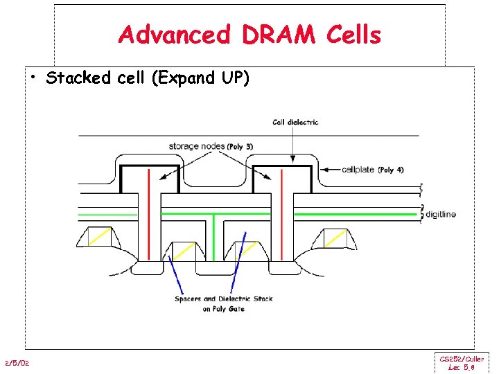 Advanced DRAM Cells • Stacked cell (Expand UP) 2/5/02 CS 252/Culler Lec 5. 8
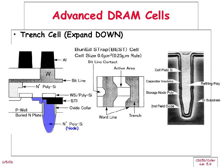 Advanced DRAM Cells • Trench Cell (Expand DOWN) 2/5/02 CS 252/Culler Lec 5. 9
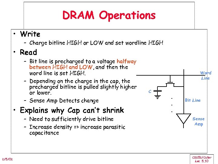 DRAM Operations • Write – Charge bitline HIGH or LOW and set wordline HIGH • Read – Bit line is precharged to a voltage halfway between HIGH and LOW, and then the word line is set HIGH. – Depending on the charge in the cap, the precharged bitline is pulled slightly higher or lower. – Sense Amp Detects change • Explains why Cap can’t shrink – Need to sufficiently drive bitline – Increase density => increase parasitic capacitance 2/5/02 Word Line C . . . Bit Line Sense Amp CS 252/Culler Lec 5. 10
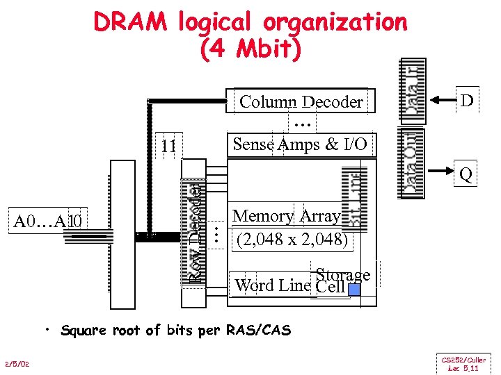 DRAM logical organization (4 Mbit) Column Decoder … Sense Amps & I/O 11 D A 0…A 10 Row Decoder … Q Memory Array (2, 048 x 2, 048) Storage Word Line Cell • Square root of bits per RAS/CAS 2/5/02 CS 252/Culler Lec 5. 11
 So, Why do I freaking care? • By it’s nature, DRAM isn’t built for speed – Reponse times dependent on capacitive circuit properties which get worse as density increases • DRAM process isn’t easy to integrate into CMOS process – DRAM is off chip – Connectors, wires, etc introduce slowness – IRAM efforts looking to integrating the two • Memory Architectures are designed to minimize impact of DRAM latency – Low Level: Memory chips – High Level memory designs. – You will pay $$$$$$ and then some $$$ for a good memory system. 2/5/02 CS 252/Culler Lec 5. 12
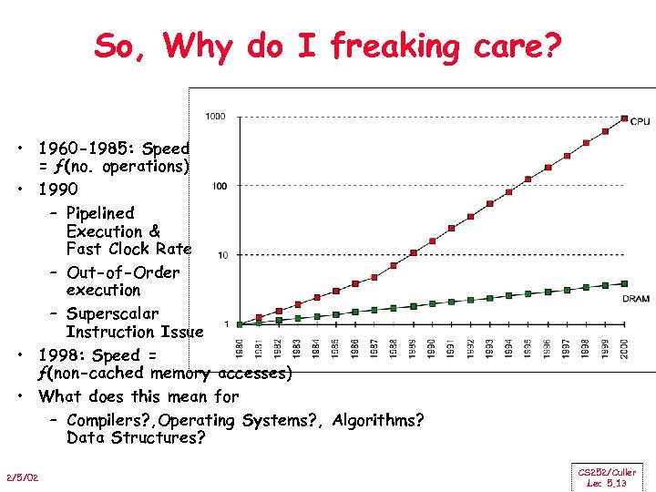 So, Why do I freaking care? • 1960 -1985: Speed = ƒ(no. operations) • 1990 – Pipelined Execution & Fast Clock Rate – Out-of-Order execution – Superscalar Instruction Issue • 1998: Speed = ƒ(non-cached memory accesses) • What does this mean for – Compilers? , Operating Systems? , Algorithms? Data Structures? 2/5/02 CS 252/Culler Lec 5. 13
 4 Key DRAM Timing Parameters • t. RAC: minimum time from RAS line falling to the valid data output. – Quoted as the speed of a DRAM when buy – A typical 4 Mb DRAM t. RAC = 60 ns – Speed of DRAM since on purchase sheet? • t. RC: minimum time from the start of one row access to the start of the next. – t. RC = 110 ns for a 4 Mbit DRAM with a t. RAC of 60 ns • t. CAC: minimum time from CAS line falling to valid data output. – 15 ns for a 4 Mbit DRAM with a t. RAC of 60 ns • t. PC: minimum time from the start of one column access to the start of the next. – 35 ns for a 4 Mbit DRAM with a t. RAC of 60 ns 2/5/02 CS 252/Culler Lec 5. 14
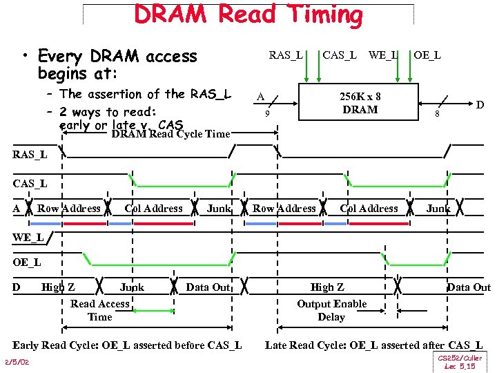 DRAM Read Timing • Every DRAM access begins at: RAS_L – The assertion of the RAS_L – 2 ways to read: early or late v. CAS A CAS_L WE_L 256 K x 8 DRAM 9 OE_L D 8 DRAM Read Cycle Time RAS_L CAS_L A Row Address Col Address Junk WE_L OE_L D High Z Junk Read Access Time Data Out Early Read Cycle: OE_L asserted before CAS_L 2/5/02 High Z Output Enable Delay Data Out Late Read Cycle: OE_L asserted after CAS_L CS 252/Culler Lec 5. 15
 DRAM Performance • A 60 ns (t. RAC) DRAM can – perform a row access only every 110 ns (t. RC) – perform column access (t. CAC) in 15 ns, but time between column accesses is at least 35 ns (t. PC). » In practice, external address delays and turning around buses make it 40 to 50 ns • These times do not include the time to drive the addresses off the microprocessor nor the memory controller overhead! • Can it be made faster? 2/5/02 CS 252/Culler Lec 5. 16
 Admin • Hand in homework assignment • New assignment is/will be on the class website. 2/5/02 CS 252/Culler Lec 5. 17
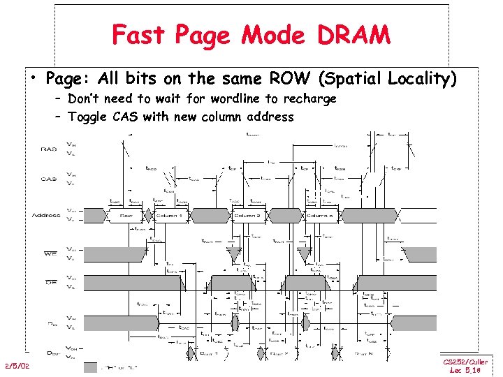 Fast Page Mode DRAM • Page: All bits on the same ROW (Spatial Locality) – Don’t need to wait for wordline to recharge – Toggle CAS with new column address 2/5/02 CS 252/Culler Lec 5. 18
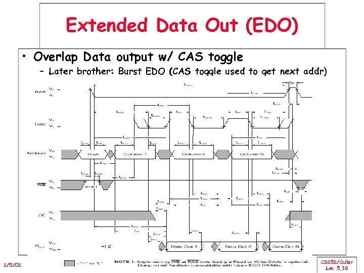 Extended Data Out (EDO) • Overlap Data output w/ CAS toggle – Later brother: Burst EDO (CAS toggle used to get next addr) 2/5/02 CS 252/Culler Lec 5. 19
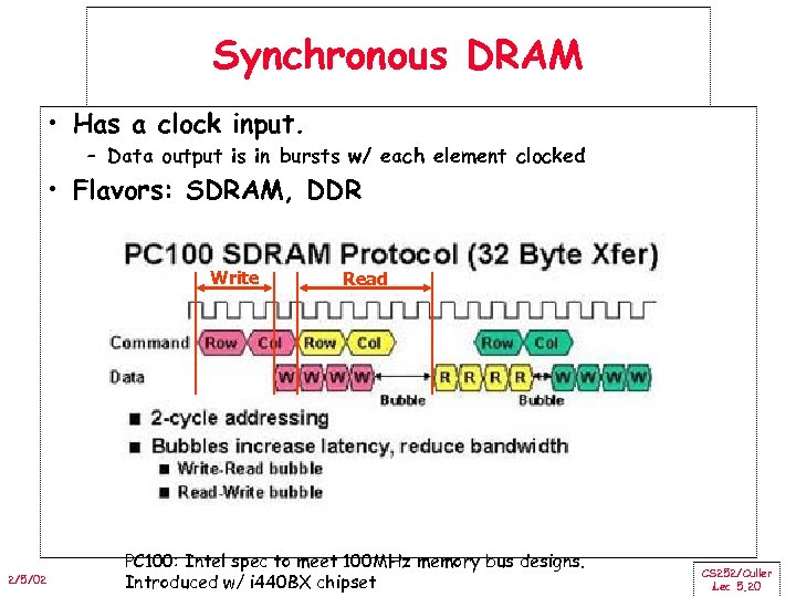 Synchronous DRAM • Has a clock input. – Data output is in bursts w/ each element clocked • Flavors: SDRAM, DDR Write 2/5/02 Read PC 100: Intel spec to meet 100 MHz memory bus designs. Introduced w/ i 440 BX chipset CS 252/Culler Lec 5. 20
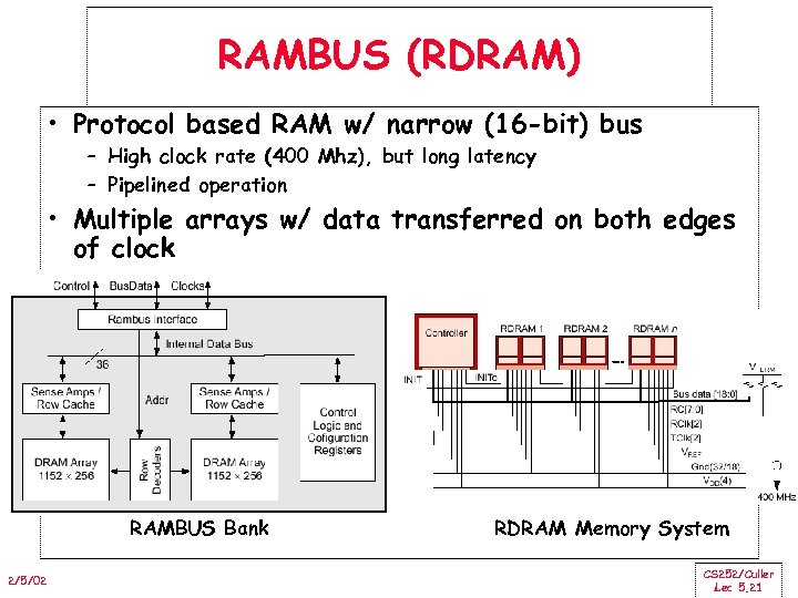 RAMBUS (RDRAM) • Protocol based RAM w/ narrow (16 -bit) bus – High clock rate (400 Mhz), but long latency – Pipelined operation • Multiple arrays w/ data transferred on both edges of clock RAMBUS Bank 2/5/02 RDRAM Memory System CS 252/Culler Lec 5. 21
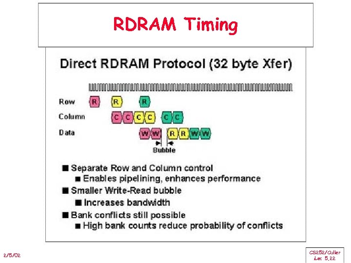 RDRAM Timing 2/5/02 CS 252/Culler Lec 5. 22
 DRAM History • DRAMs: capacity +60%/yr, cost – 30%/yr – 2. 5 X cells/area, 1. 5 X die size in 3 years • ‘ 98 DRAM fab line costs $2 B – DRAM only: density, leakage v. speed • Rely on increasing no. of computers & memory per computer (60% market) – SIMM or DIMM is replaceable unit => computers use any generation DRAM • Commodity, second source industry => high volume, low profit, conservative – Little organization innovation in 20 years – Don’t want to be chip foundries (bad for RDRAM) • Order of importance: 1) Cost/bit 2) Capacity – First RAMBUS: 10 X BW, +30% cost => little impact 2/5/02 CS 252/Culler Lec 5. 23
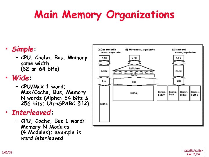 Main Memory Organizations • Simple: – CPU, Cache, Bus, Memory same width (32 or 64 bits) • Wide: – CPU/Mux 1 word; Mux/Cache, Bus, Memory N words (Alpha: 64 bits & 256 bits; Utra. SPARC 512) • Interleaved: – CPU, Cache, Bus 1 word: Memory N Modules (4 Modules); example is word interleaved 2/5/02 CS 252/Culler Lec 5. 24
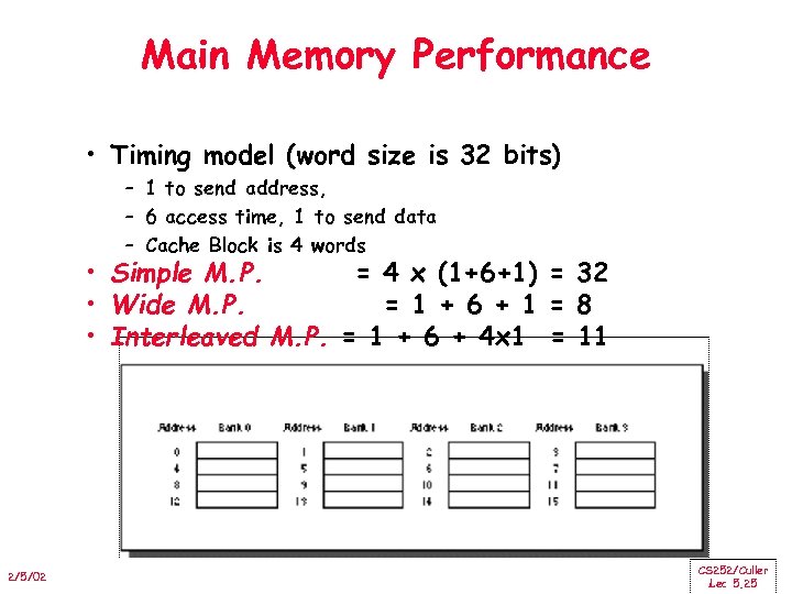 Main Memory Performance • Timing model (word size is 32 bits) – 1 to send address, – 6 access time, 1 to send data – Cache Block is 4 words • Simple M. P. = 4 x (1+6+1) = 32 • Wide M. P. = 1 + 6 + 1 = 8 • Interleaved M. P. = 1 + 6 + 4 x 1 = 11 2/5/02 CS 252/Culler Lec 5. 25
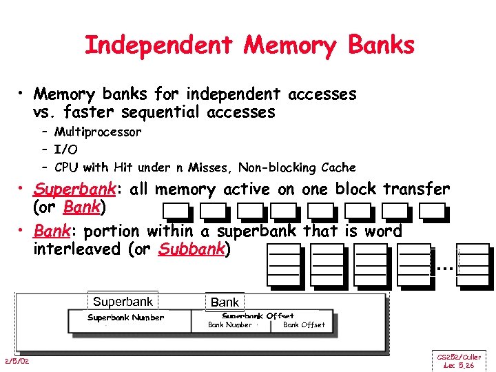 Independent Memory Banks • Memory banks for independent accesses vs. faster sequential accesses – Multiprocessor – I/O – CPU with Hit under n Misses, Non-blocking Cache • Superbank: all memory active on one block transfer (or Bank) • Bank: portion within a superbank that is word interleaved (or Subbank) … Superbank Number 2/5/02 Bank Superbank Offset Bank Number Bank Offset CS 252/Culler Lec 5. 26
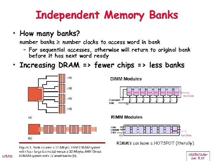 Independent Memory Banks • How many banks? number banks number clocks to access word in bank – For sequential accesses, otherwise will return to original bank before it has next word ready • Increasing DRAM => fewer chips => less banks RIMM’s can have a HOTSPOT (literally) 2/5/02 CS 252/Culler Lec 5. 27
![Avoiding Bank Conflicts • Lots of banks int x[256][512]; for (j = 0; j Avoiding Bank Conflicts • Lots of banks int x[256][512]; for (j = 0; j](https://present5.com/presentation/33a614ca543a56bb413e8241a5f4dc86/image-28.jpg) Avoiding Bank Conflicts • Lots of banks int x[256][512]; for (j = 0; j < 512; j = j+1) for (i = 0; i < 256; i = i+1) x[i][j] = 2 * x[i][j]; • Even with 128 banks, since 512 is multiple of 128, conflict on word accesses • SW: loop interchange or declaring array not power of 2 (“array padding”) • HW: Prime number of banks – – – 2/5/02 bank number = address mod number of banks address within bank = address / number of words in bank modulo & divide per memory access with prime no. banks? address within bank = address mod number words in bank number? easy if 2 N words per bank CS 252/Culler Lec 5. 28
Avoiding Bank Conflicts • Lots of banks int x[256][512]; for (j = 0; j < 512; j = j+1) for (i = 0; i < 256; i = i+1) x[i][j] = 2 * x[i][j]; • Even with 128 banks, since 512 is multiple of 128, conflict on word accesses • SW: loop interchange or declaring array not power of 2 (“array padding”) • HW: Prime number of banks – – – 2/5/02 bank number = address mod number of banks address within bank = address / number of words in bank modulo & divide per memory access with prime no. banks? address within bank = address mod number words in bank number? easy if 2 N words per bank CS 252/Culler Lec 5. 28
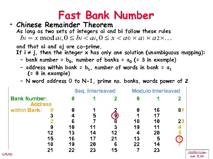 Fast Bank Number • Chinese Remainder Theorem As long as two sets of integers ai and bi follow these rules and that ai and aj are co-prime. If i j, then the integer x has only one solution (unambiguous mapping): – bank number = b 0, number of banks = a 0 (= 3 in example) – address within bank = b 1, number of words in bank = a 1 (= 8 in example) – N word address 0 to N-1, prime no. banks, words power of 2 Bank Number: Address within Bank: 0 3 2 9 12 15 18 21 2/5/02 Seq. Interleaved 0 1 2 0 4 6 10 13 16 19 22 1 5 7 11 14 17 20 23 2 9 8 3 12 21 6 15 Modulo Interleaved 0 1 2 0 1 18 19 4 13 22 7 16 17 10 11 20 5 14 23 81 23 4 5 6 7 CS 252/Culler Lec 5. 29
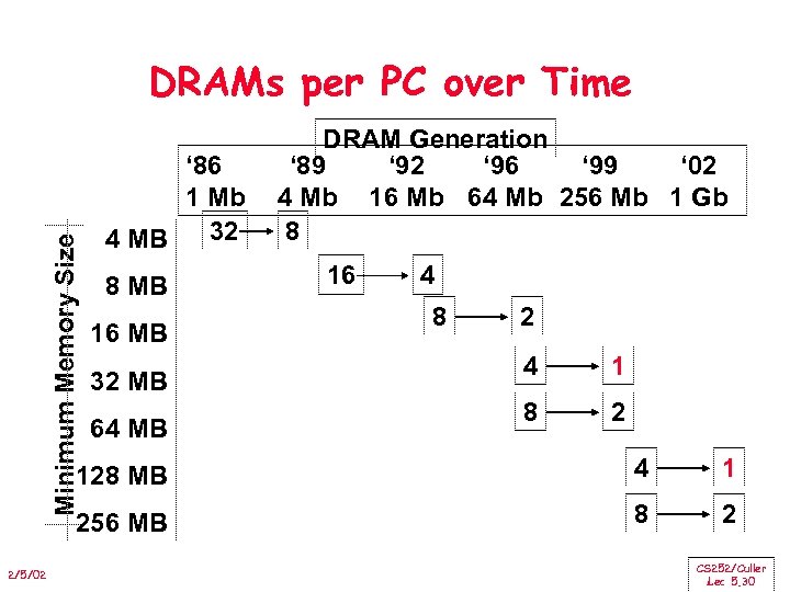 Minimum Memory Size DRAMs per PC over Time ‘ 86 1 Mb 32 4 MB 8 MB 16 MB 32 MB 64 MB DRAM Generation ‘ 89 ‘ 92 ‘ 96 ‘ 99 ‘ 02 4 Mb 16 Mb 64 Mb 256 Mb 1 Gb 8 16 4 8 2 4 1 8 2 128 MB 1 256 MB 2/5/02 4 8 2 CS 252/Culler Lec 5. 30
 Need for Error Correction! • Motivation: – Failures/time proportional to number of bits! – As DRAM cells shrink, more vulnerable • Went through period in which failure rate was low enough without error correction that people didn’t do correction – DRAM banks too large now – Servers always corrected memory systems • Basic idea: add redundancy through parity bits – Simple but wastful version: » Keep three copies of everything, vote to find right value » 200% overhead, so not good! – Common configuration: Random error correction » SEC-DED (single error correct, double error detect) » One example: 64 data bits + 8 parity bits (11% overhead) » Papers up on reading list from last term tell you how to do these types of codes – Really want to handle failures of physical components as well » Organization is multiple DRAMs/SIMM, multiple SIMMs » Want to recover from failed DRAM and failed SIMM! » Requires more redundancy to do this » All major vendors thinking about this in high-end machines 2/5/02 CS 252/Culler Lec 5. 31
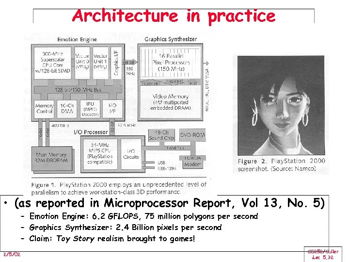 Architecture in practice • (as reported in Microprocessor Report, Vol 13, No. 5) – Emotion Engine: 6. 2 GFLOPS, 75 million polygons per second – Graphics Synthesizer: 2. 4 Billion pixels per second – Claim: Toy Story realism brought to games! 2/5/02 CS 252/Culler Lec 5. 32
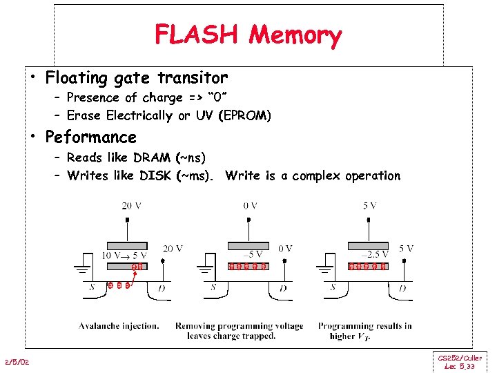 FLASH Memory • Floating gate transitor – Presence of charge => “ 0” – Erase Electrically or UV (EPROM) • Peformance – Reads like DRAM (~ns) – Writes like DISK (~ms). Write is a complex operation 2/5/02 CS 252/Culler Lec 5. 33
 More esoteric Storage Technologies? • Tunneling Magnetic Junction RAM (TMJ-RAM): – Speed of SRAM, density of DRAM, non-volatile (no refresh) – New field called “Spintronics”: combination of quantum spin and electronics – Same technology used in high-density disk-drives • MEMs storage devices: – Large magnetic “sled” floating on top of lots of little read/write heads – Micromechanical actuators move the sled back and forth over the heads 2/5/02 CS 252/Culler Lec 5. 34
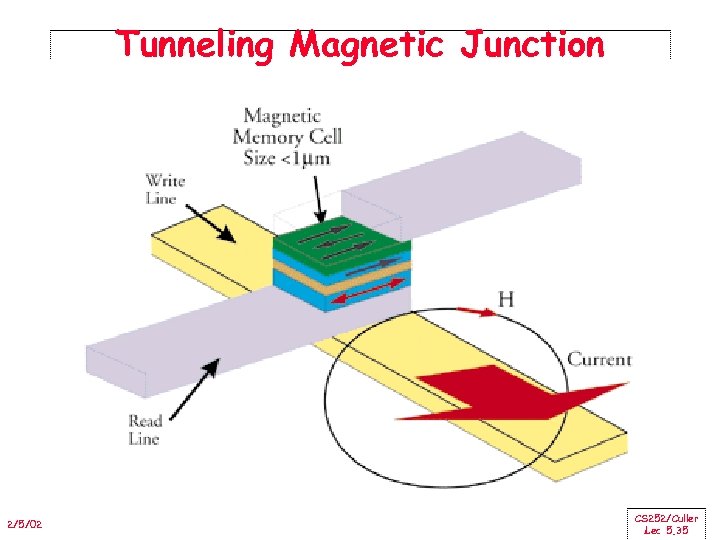 Tunneling Magnetic Junction 2/5/02 CS 252/Culler Lec 5. 35
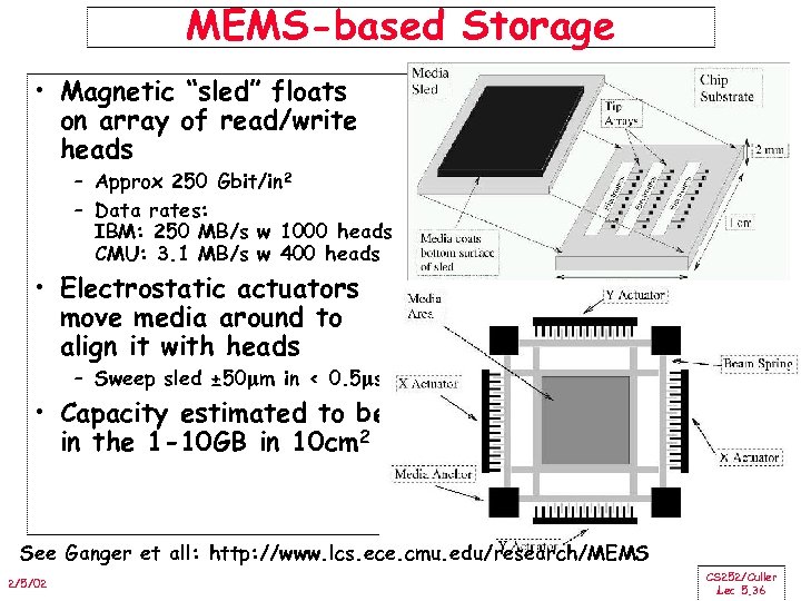 MEMS-based Storage • Magnetic “sled” floats on array of read/write heads – Approx 250 Gbit/in 2 – Data rates: IBM: 250 MB/s w 1000 heads CMU: 3. 1 MB/s w 400 heads • Electrostatic actuators move media around to align it with heads – Sweep sled ± 50 m in < 0. 5 s • Capacity estimated to be in the 1 -10 GB in 10 cm 2 See Ganger et all: http: //www. lcs. ece. cmu. edu/research/MEMS 2/5/02 CS 252/Culler Lec 5. 36
 Main Memory Summary • Wider Memory • Interleaved Memory: for sequential or independent accesses • Avoiding bank conflicts: SW & HW • DRAM specific optimizations: page mode & Specialty DRAM • Need Error correction 2/5/02 CS 252/Culler Lec 5. 37


