6d08b35c6c4fc9c753582d5259dd3c1b.ppt
- Количество слайдов: 80

CREDES Summer School Dependable Systems Design June 2 -3, 2011. Tallinn University of Technology, Estonia Fault Modeling and Diagnosis in Digital Systems Raimund Ubar
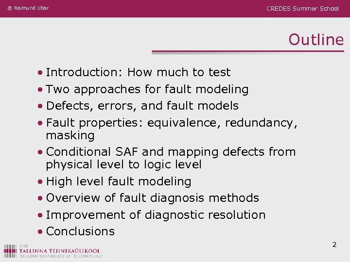
© Raimund Ubar CREDES Summer School Outline • Introduction: How much to test • Two approaches for fault modeling • Defects, errors, and fault models • Fault properties: equivalence, redundancy, masking • Conditional SAF and mapping defects from physical level to logic level • High level fault modeling • Overview of fault diagnosis methods • Improvement of diagnostic resolution • Conclusions 2

© Raimund Ubar CREDES Summer School Introduction: Search for the Quality Yield (Y) P, n Design for testability Testing Quality policy Defect level (DL) Pa P - probability of a defect n - number of defects Pa - probability of accepting a bad product - probability of producing a good product 3
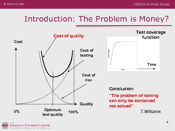
© Raimund Ubar CREDES Summer School Introduction: The Problem is Money? Test coverage function Cost of quality Cost of testing Time Cost of risc Conclusion: Quality 0% Optimum test quality 100% “The problem of testing can only be contained not solved” T. Williams 4
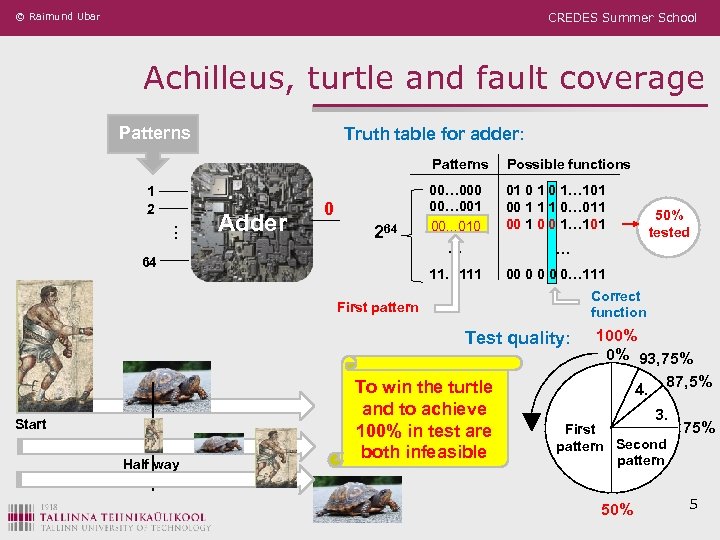
© Raimund Ubar CREDES Summer School Achilleus, turtle and fault coverage Patterns Truth table for adder: Patterns . . . 1 2 Adder 0 264 64 Possible functions 00… 000 00… 001 00… 010 00. . . 010 01 0 1… 101 00 1 1 1 0… 011 00 1 0 0 1… 101 … … 111 00 0 0… 111 Correct function First pattern Test quality: Start Half way 50% tested To win the turtle and to achieve 100% in test are both infeasible 100% 0% 93, 75% 87, 5% 4. 3. First pattern Second pattern 50% 75% 5
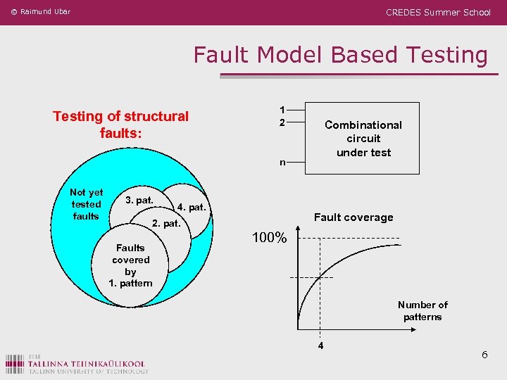
© Raimund Ubar CREDES Summer School Fault Model Based Testing of structural faults: 1 2 Combinational circuit under test n Not yet tested faults 3. pat. 4. pat. Fault coverage 2. pat. Faults covered by 1. pattern 100% Number of patterns 4 6
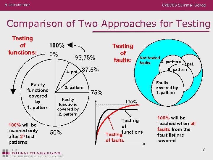
© Raimund Ubar CREDES Summer School Comparison of Two Approaches for Testing of functions: 100% 0% 93, 75% 4. pat. Faulty functions covered by 1. pattern 100% will be reached only after 2 n test patterns 87, 5% 3. pattern Faulty functions covered by 2. pattern 50% Testing of faults: Not tested 3. patttern faults 4. pat. 2. pattern Faults covered by 1. pattern 75% 100% Testing of functions Testing of faults 100% will be reached when all faults from the fault list are covered 7
© Raimund Ubar CREDES Summer School Physical Defects as Fault Causes Physical defects may occur: • Manufacturing process: missing contacts , parasitic transistors, gate oxide shorts, oxide break-down, metal-to silicon shorts, missing or wrong components, broken or shorted tracks (board design), etc. • Process fabrication marginalities: line width variation, etc. • Material and age defects: bulk defects (cracks, crystal imperfections), surface impurities, dielectric breakdown, electromigration, etc. • Packaging: contact degradation, seal leaks, etc. • Enviromental infuence: temperature related defects, high humidity, vibration, electrical stress, crosstalk, radiation, etc. 8
© Raimund Ubar CREDES Summer School Soft and Hard Defects can be divided roughly into two basic groups : • Soft defects • defects which cause speed fault • show up at high speed or produce some temperature • they need two or more test patterns for their activation and error observation (require carefully constructed transitions for defect activation); • require tests to be applied at speed. • examples: “high resistance” bridges, x-coupling, “tunneling break” • Hard defects • • defects observated at all frequencies a test can be applied at slow speed they need only one-pattern test set example: “low resistance” bridge 9
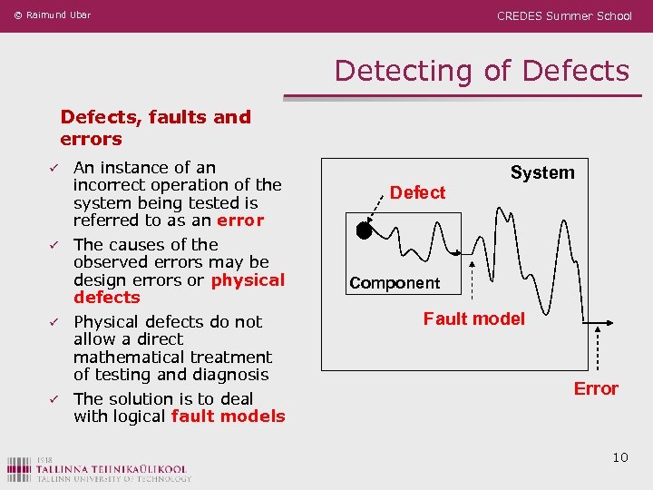
© Raimund Ubar CREDES Summer School Detecting of Defects, faults and errors ü ü An instance of an incorrect operation of the system being tested is referred to as an error The causes of the observed errors may be design errors or physical defects Physical defects do not allow a direct mathematical treatment of testing and diagnosis The solution is to deal with logical fault models Defect System Component Fault model Error 10

© Raimund Ubar CREDES Summer School Defect Manifestation and Test Methods Defects have to be measured and modeled into the faults They are manifested in different measurable manners: • by changing a logical value on a circuit node (Boolean testing, or testing at the logical level) • by increasing the steady state supply current (IDDQ testing) • by changing time specifications (At-speed testing) • by variation in one or a set of parameters such that their specific distribution in a circuit makes it fall out of specifications The test methods listed are not replacable They all have to be used for achieving high quality of testing 11

© Raimund Ubar CREDES Summer School Why We Need Fault Models? • Fault models are needed for • test generation, • test quality evaluation and • fault diagnosis • To handle real physical defects is too difficult • The fault model should • reflect accurately the behaviour of defects, and • be computationably efficient • Usually combination of different fault models is used • Fault model free approaches (!) 12
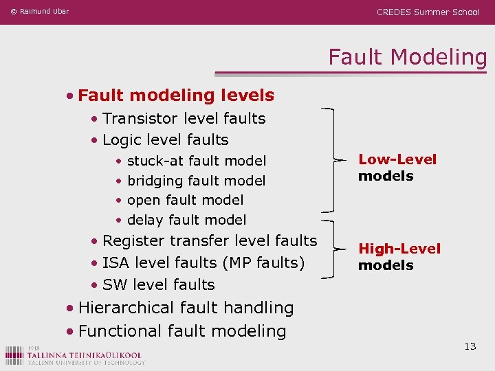
© Raimund Ubar CREDES Summer School Fault Modeling • Fault modeling levels • Transistor level faults • Logic level faults • • stuck-at fault model bridging fault model open fault model delay fault model • Register transfer level faults • ISA level faults (MP faults) • SW level faults • Hierarchical fault handling • Functional fault modeling Low-Level models High-Level models 13
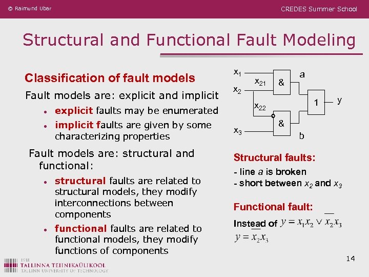
© Raimund Ubar CREDES Summer School Structural and Functional Fault Modeling Classification of fault models Fault models are: explicit and implicit · implicit faults are given by some characterizing properties x 2 Fault models are: structural and functional: · · structural faults are related to structural models, they modify interconnections between components functional faults are related to functional models, they modify functions of components x 21 & a 1 x 22 explicit faults may be enumerated · x 1 x 3 y & b Structural faults: - line a is broken - short between x 2 and x 3 Functional fault: Instead of 14

© Raimund Ubar CREDES Summer School Structural Logic Level Fault Modeling Why logic fault models? ü complexity of simulation reduces (many physical faults may be modeled by the same logic fault) ü one logic fault model is applicable to many technologies ü logic fault tests may be used for physical faults whose effect is not completely understood ü they give a possibility to move from the lower physical level to the higher logic level Stuck-at fault model: Two defects: Broken line Bridge to ground x 1 x 2 1 Single model: Stuck-at-0 x 2 1 0 V 15
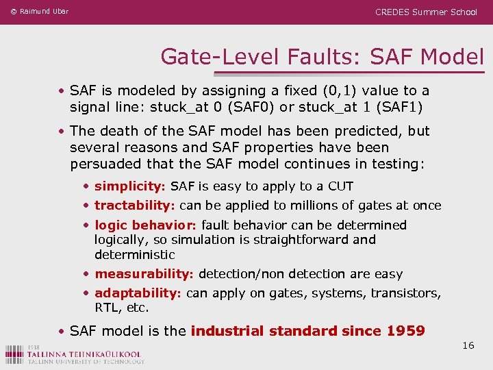
© Raimund Ubar CREDES Summer School Gate-Level Faults: SAF Model • SAF is modeled by assigning a fixed (0, 1) value to a signal line: stuck_at 0 (SAF 0) or stuck_at 1 (SAF 1) • The death of the SAF model has been predicted, but several reasons and SAF properties have been persuaded that the SAF model continues in testing: • simplicity: SAF is easy to apply to a CUT • tractability: can be applied to millions of gates at once • logic behavior: fault behavior can be determined logically, so simulation is straightforward and deterministic • measurability: detection/non detection are easy • adaptability: can apply on gates, systems, transistors, RTL, etc. • SAF model is the industrial standard since 1959 16
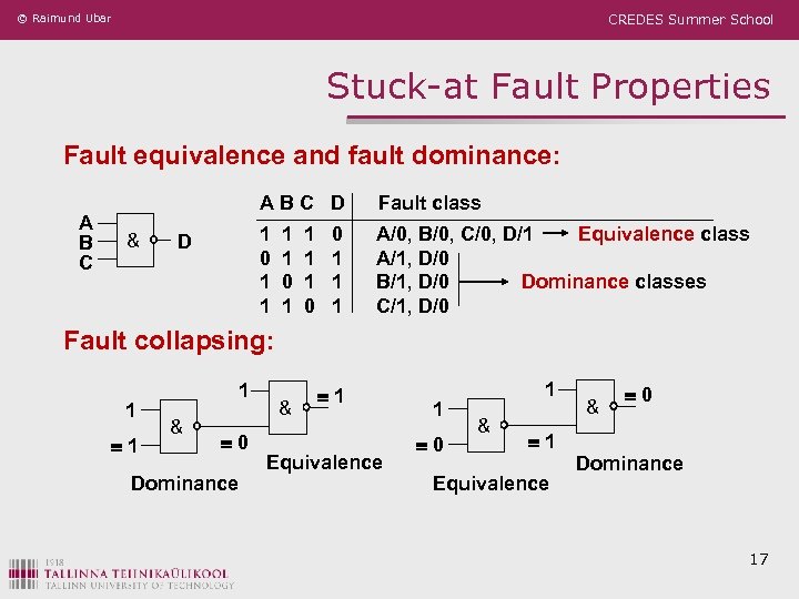
© Raimund Ubar CREDES Summer School Stuck-at Fault Properties Fault equivalence and fault dominance: A B C ABC D & 1 0 1 1 D Fault class A/0, B/0, C/0, D/1 Equivalence class A/1, D/0 B/1, D/0 Dominance classes C/1, D/0 1 1 1 1 0 0 1 1 1 Fault collapsing: 1 1 1 & 0 Dominance & 1 Equivalence 1 0 1 & 1 Equivalence & 0 Dominance 17
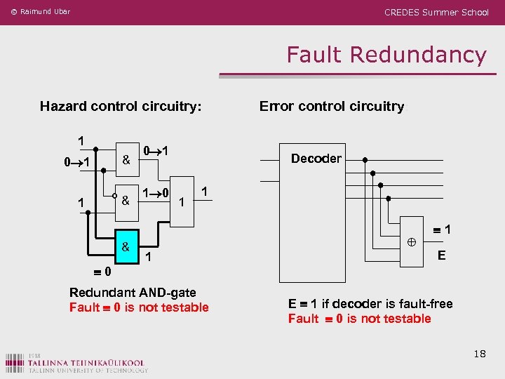
© Raimund Ubar CREDES Summer School Fault Redundancy Hazard control circuitry: 1 & 0 0 1 1 0 Error control circuitry: Decoder 1 1 1 Redundant AND-gate Fault 0 is not testable 1 E E 1 if decoder is fault-free Fault 0 is not testable 18
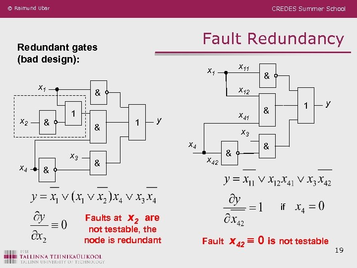
© Raimund Ubar CREDES Summer School Fault Redundancy Redundant gates (bad design): x 11 x 1 x 2 & & x 3 x 4 & x 12 & 1 x 41 y Faults at x 2 are not testable, the node is redundant & y x 3 x 4 & 1 x 42 & & if Fault x 42 0 is not testable 19
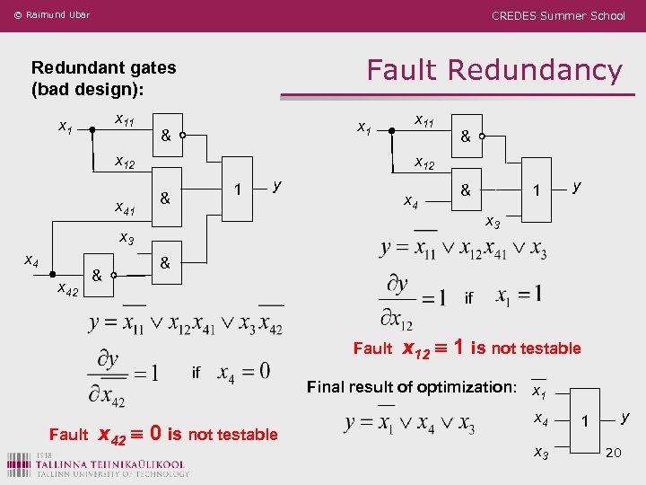
© Raimund Ubar CREDES Summer School Fault Redundancy Redundant gates (bad design): x 11 x 1 & x 12 x 41 x 11 & x 12 1 & y x 4 & x 42 & & if Fault y x 3 x 4 1 x 42 0 is not testable x 12 1 is not testable Final result of optimization: x 1 x 4 x 3 1 y 20
© Raimund Ubar CREDES Summer School Delay Faults ü Studies of the electrical properties of defects have shown that most of the random CMOS defects cause a timing (delay) effect rather than a other catastrophic defects (e. g. resistive bridges above a critical resistance cause delay) ü Delay fault means that a good CUT may perform correctly its function in a system, but it fails in designed timing specifications ü Delay faults could be caused by: n n subtle manufacturing process defects, transistor threshold voltage shifts, increased parasitic capacitance, improper timing design, etc. 21
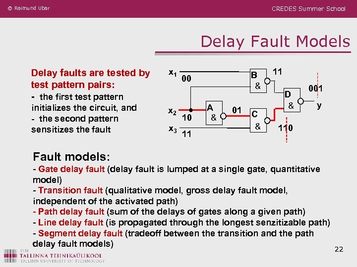
© Raimund Ubar CREDES Summer School Delay Fault Models Delay faults are tested by test pattern pairs: - the first test pattern x 1 initializes the circuit, and - the second pattern sensitizes the fault x 2 x 3 B & 00 10 11 A & 01 C & 11 D & 001 y 110 Fault models: - Gate delay fault (delay fault is lumped at a single gate, quantitative model) - Transition fault (qualitative model, gross delay fault model, independent of the activated path) - Path delay fault (sum of the delays of gates along a given path) - Line delay fault (is propagated through the longest senzitizable path) - Segment delay fault (tradeoff between the transition and the path delay fault models) 22
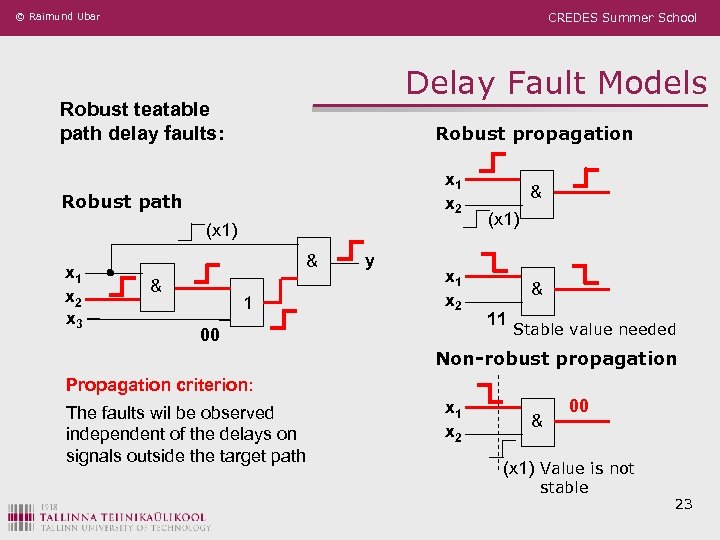
© Raimund Ubar CREDES Summer School Delay Fault Models Robust teatable path delay faults: Robust propagation x 1 x 2 Robust path (x 1) x 1 x 2 x 3 & & 1 y x 1 x 2 00 & (x 1) & 11 Stable value needed Non-robust propagation Propagation criterion: The faults wil be observed independent of the delays on signals outside the target path x 1 x 2 & 00 (x 1) Value is not stable 23
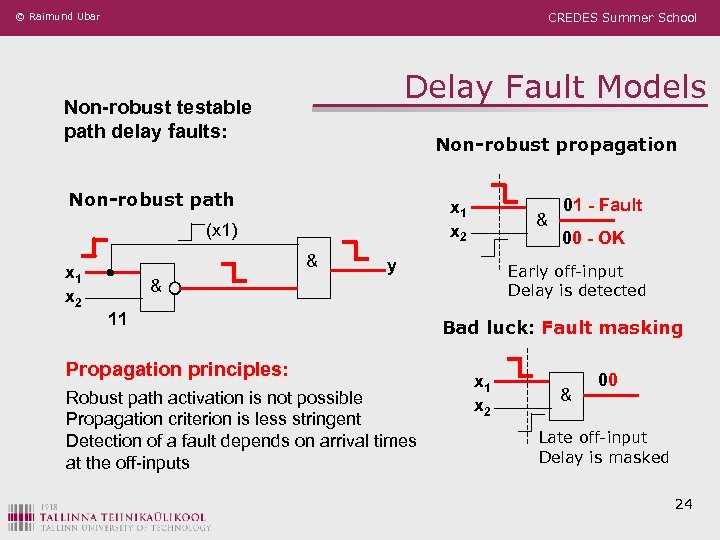
© Raimund Ubar CREDES Summer School Delay Fault Models Non-robust testable path delay faults: Non-robust propagation Non-robust path x 1 x 2 (x 1) x 1 x 2 & & y 00 - OK Early off-input Delay is detected & 11 01 - Fault Bad luck: Fault masking Propagation principles: Robust path activation is not possible Propagation criterion is less stringent Detection of a fault depends on arrival times at the off-inputs x 1 x 2 & 00 Late off-input Delay is masked 24
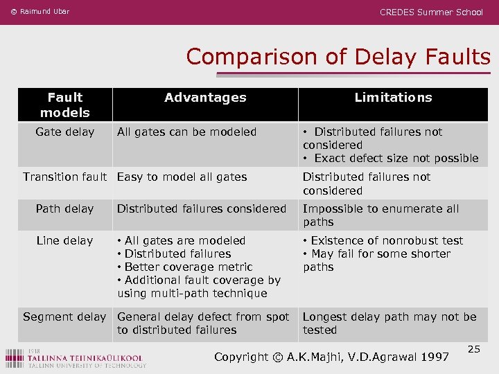
© Raimund Ubar CREDES Summer School Comparison of Delay Faults Fault models Gate delay Advantages All gates can be modeled Transition fault Easy to model all gates Limitations • Distributed failures not considered • Exact defect size not possible Distributed failures not considered Path delay Distributed failures considered Impossible to enumerate all paths Line delay • All gates are modeled • Distributed failures • Better coverage metric • Additional fault coverage by using multi-path technique • Existence of nonrobust test • May fail for some shorter paths Segment delay General delay defect from spot to distributed failures Longest delay path may not be tested Copyright © A. K. Majhi, V. D. Agrawal 1997 25

© Raimund Ubar CREDES Summer School Multiple Fault Problem ü ü ü Multiple stuck-fault (MSF) model is a straightforward extension of the single stuck-fault (SSF) model where several lines can be simultaneously stuck If n - is the number of possible SSF sites, there are 2 n possible SSFs, but there are 3 n -1 possible MSFs If we assume that the multiplicity of faults is no greater than k , then the number of possible MSFs is ki=1 {Cni}2 i {Cni} – number of sets of lines, 2 i - number of faults of the set ü The number of multiple faults is very big. However, their consideration is needed because of possible fault masking 26
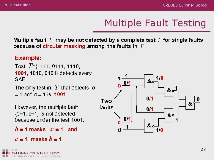
© Raimund Ubar CREDES Summer School Multiple Fault Testing Multiple fault F may be not detected by a complete test T for single faults because of circular masking among the faults in F Example: Test T={1111, 0111, 1110, 1001, 1010, 0101} detects every SAF a 1 0/1 b The only test in T that detects b 1 and c 1 is 1001 However, the multiple fault {b 1, c 1} is not detected because under the test 1001, b 1 masks c 1, c 1 masks b 1 and & 1/0 & 1 0/1 Two faults & 0/1 c 1 d & & 0 1 1/0 27
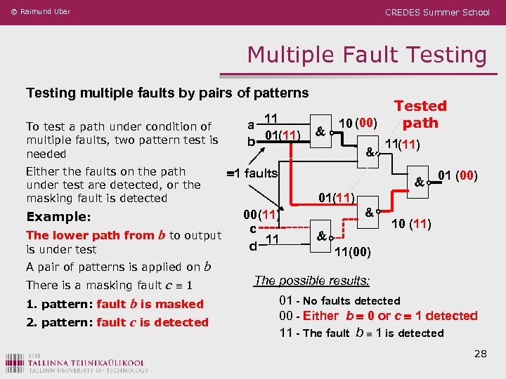
© Raimund Ubar CREDES Summer School Multiple Fault Testing multiple faults by pairs of patterns To test a path under condition of multiple faults, two pattern test is needed Either the faults on the path under test are detected, or the masking fault is detected There is a masking fault b c 1 b is masked 2. pattern: fault c is detected 1. pattern: fault 10 (00) & 11(11) & 01 (00) 01(11) b to output A pair of patterns is applied on & 1 faults Example: The lower path from is under test a 11 01(11) b Tested path 00 (11) c 11 d & & 10 (11) 11(00) The possible results: 01 - No faults detected 00 - Either b 0 or c 1 detected 11 - The fault b 1 is detected 28
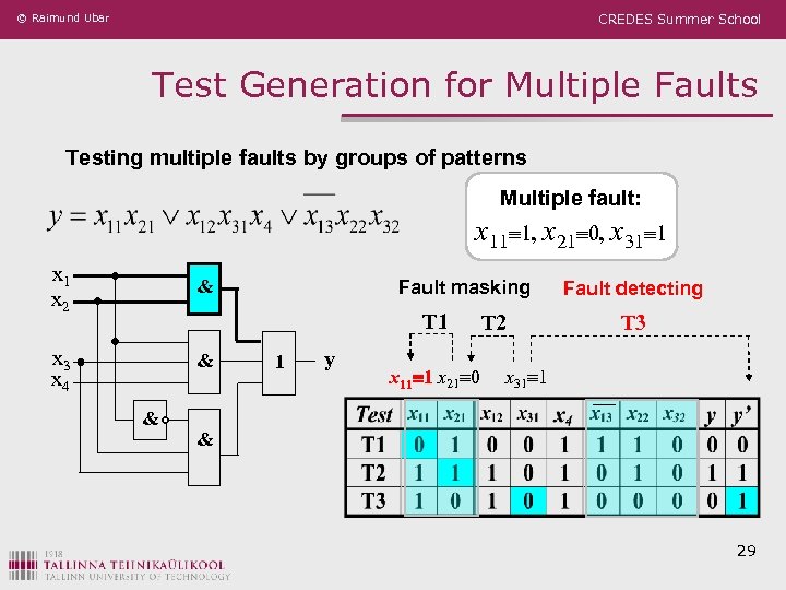
© Raimund Ubar CREDES Summer School Test Generation for Multiple Faults Testing multiple faults by groups of patterns Multiple fault: x 11 1, x 21 0, x 31 1 x 2 & x 3 x 4 & Fault masking T 1 & 1 y x 11 1 x 21 0 T 2 Fault detecting T 3 x 31 1 & 29
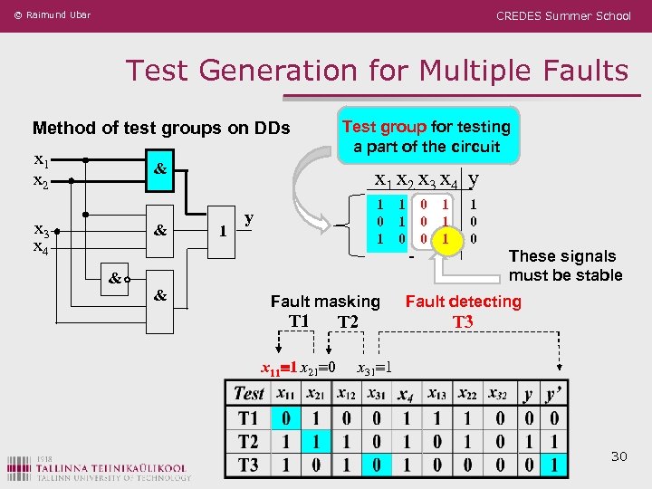
© Raimund Ubar CREDES Summer School Test Generation for Multiple Faults Method of test groups on DDs x 1 x 2 Test group for testing a part of the circuit & x 3 x 4 & & & x 1 x 2 x 3 x 4 y 1 1 1 0 1 0 1 1 0 0 1 - y Fault masking T 1 x 11 1 x 21 0 T 2 1 0 0 These signals must be stable Fault detecting T 3 x 31 1 30
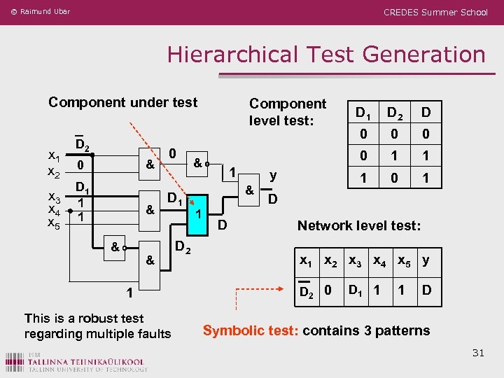
© Raimund Ubar CREDES Summer School Hierarchical Test Generation Component under test x 1 x 2 x 3 x 4 x 5 D 2 & 0 D 1 1 1 & & 0 D 1 & 1 This is a robust test regarding multiple faults D 2 Component level test: 1 & 1 D D 0 0 0 1 1 1 y D 2 0 & D 1 0 1 D Network level test: x 1 x 2 x 3 x 4 x 5 y D 2 0 D 1 1 1 D Symbolic test: contains 3 patterns 31
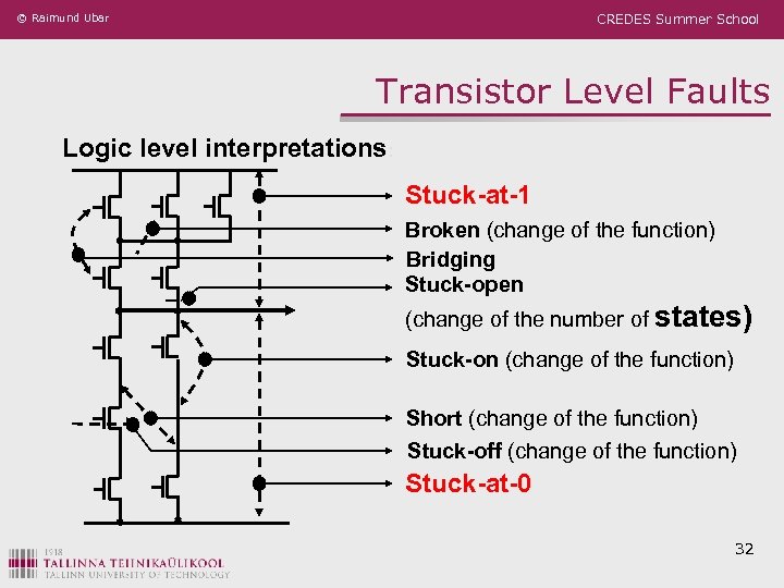
© Raimund Ubar CREDES Summer School Transistor Level Faults Logic level interpretations: Stuck-at-1 Broken (change of the function) Bridging Stuck-open (change of the number of states) Stuck-on (change of the function) Short (change of the function) Stuck-off (change of the function) Stuck-at-0 32
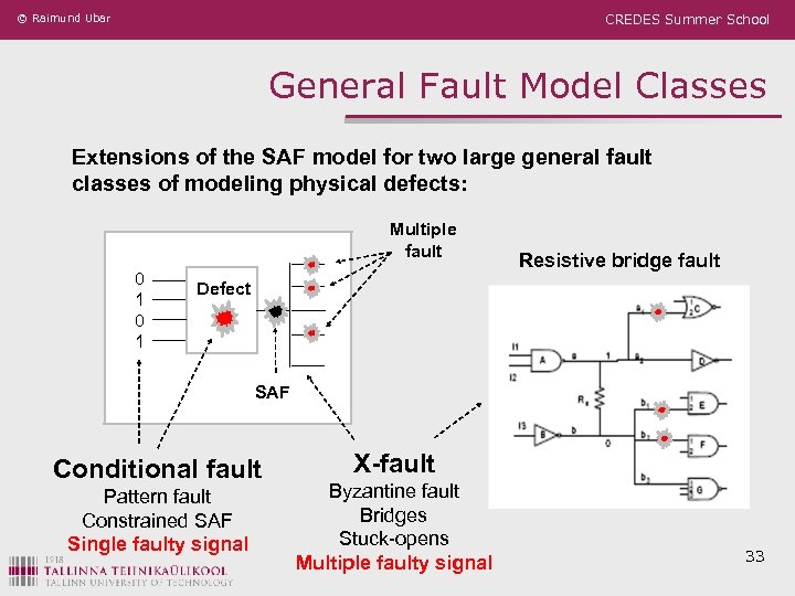
© Raimund Ubar CREDES Summer School General Fault Model Classes Extensions of the SAF model for two large general fault classes of modeling physical defects: Multiple fault 0 1 Resistive bridge fault Defect SAF Conditional fault Pattern fault Constrained SAF Single faulty signal X-fault Byzantine fault Bridges Stuck-opens Multiple faulty signal 33

© Raimund Ubar CREDES Summer School Mapping Transistor Faults to Logic Level A transistor fault causes a change in a logic function not representable by SAF model Function: y Faulty function: x 1 x 4 Short Defect variable: x 2 x 3 d= Generic function with defect: 0 – defect d is missing 1 – defect d is present x 5 Mapping the physical defect onto the logic level by solving the equation: 34

© Raimund Ubar CREDES Summer School Mapping Transistor Faults to Logic Level Function: Faulty function: Generic function with defect: y x 1 x 4 Short Test calculation by Boolean derivative: x 2 x 3 x 5 35

© Raimund Ubar CREDES Summer School Transistor Level Stuck-On Faults NOR gate VDD x 1 Stuck-on x 1 x 2 Y x 1 x 2 1 1 0 0 VY/IDDQ 1 0 0 Y x 1 VSS 1 1 RN 0 1 x 2 yd 0 x 1 y 0 VDD x 2 RP x 2 VSS Conducting path for “ 10” 36
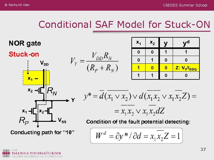
© Raimund Ubar CREDES Summer School Conditional SAF Model for Stuck-ON NOR gate x 1 x 2 y yd Stuck-on 0 0 1 1 0 0 Z: VY/IDDQ 1 1 0 0 VDD x 1 RN x 2 Y x 1 RP x 2 VSS Condition of the fault potential detecting: Conducting path for “ 10” 37

© Raimund Ubar CREDES Summer School Transistor Level Stuck-open Faults NOR gate VDD x 1 Stuck-open y yd 0 0 1 1 0 VDD x 2 1 0 0 x 1 1 0 0 Y’ x 2 1 1 0 0 Y x 1 x 2 Y x 1 VSS x 2 VSS Test sequence is needed: 00, 10 No conducting path from VDD to VSS for “ 10” 38
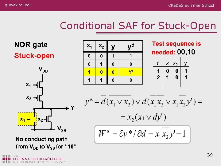
© Raimund Ubar CREDES Summer School Conditional SAF for Stuck-Open NOR gate Stuck-open x 1 yd 0 1 1 0 0 Y’ 1 x 1 y 0 VDD x 2 1 0 0 Test sequence is needed: 00, 10 t x 1 x 2 y 1 0 0 1 2 1 0 1 x 2 Y x 1 x 2 VSS No conducting path from VDD to VSS for “ 10” 39
© Raimund Ubar CREDES Summer School Bridging Faults ü Bridging faults model all defects that cause unintended electrical connections across two or more circuit nodes ü Physical causes of the shorts: n n ü extra conducting material: e. g. photolitographic printing error, conductive particle contamination, etc. missing insulating material: printing error, gate-oxide defect causing pinhole, insulating particle contamination, etc. Bridges have non-linear or linear properties with resistance from zero to > 1 MΩ. The typical values for resistance: n n ü logical critical resistance is 100 Ω to 2 kΩ timing critical resistance is 5 kΩ to 10 kΩ Bridging faults can be classified: n inter-gate shorts (sequential behavior if short creates feedback) n intra-gate shorts 40
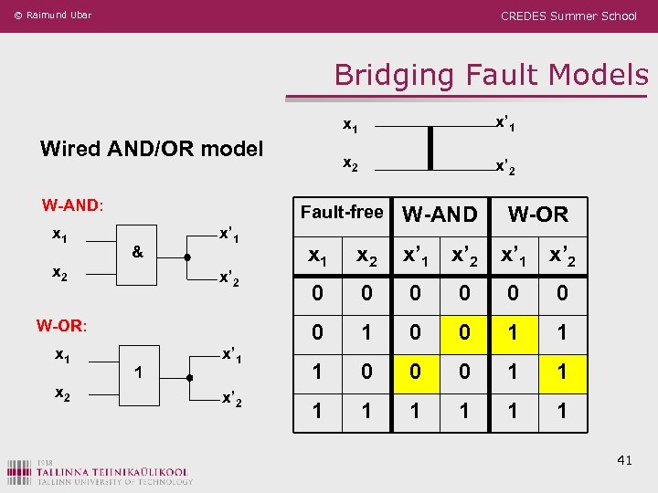
© Raimund Ubar CREDES Summer School Bridging Fault Models x 1 x 2 Wired AND/OR model W-AND: x 1 & x’ 1 x’ 2 W-OR: x 2 x’ 2 Fault-free x 2 x 1 x’ 2 W-AND W-OR x 1 x 2 x’ 1 x’ 2 0 0 0 0 1 1 1 0 0 0 1 1 1 1 41
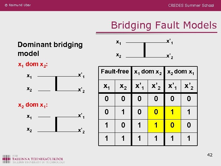
© Raimund Ubar CREDES Summer School Bridging Fault Models x 1 x 2 Dominant bridging model x 1 dom x 2: x 1 x’ 1 x 2 x’ 2 Fault-free x 1 dom x 2 dom x 1 x’ 2 x 1 x 2 x’ 1 x’ 2 0 x 2 dom x 1: x 1 x’ 1 0 0 0 1 1 1 0 0 1 1 1 42

© Raimund Ubar CREDES Summer School Conditional SAF Model for Bridging Example: Bridging fault x*k xk xl between leads xk and xl d xk*= f(xk, xl, d) The condition means that in order to detect the short between leads on the lead Wired. AND model xk we have to assign to xk xk the value 1 and to xl and xl the value 0. 43
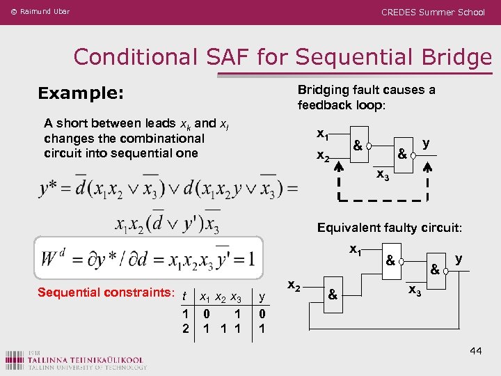
© Raimund Ubar CREDES Summer School Conditional SAF for Sequential Bridge Example: Bridging fault causes a feedback loop: A short between leads xk and xl changes the combinational circuit into sequential one x 1 x 2 & y & x 3 Equivalent faulty circuit: x 1 Sequential constraints: t x 1 x 2 x 3 y 1 0 2 1 1 x 2 & & & y x 3 44

© Raimund Ubar CREDES Summer School Simulating of Bridging Faults ü In absence of any physical layout information, a fault list may be created by exhaustively enumerating every two nets in the design ü This method, however, is only feasible for very small circuits, because the number of all net pairs in the design grows exponentially ü For larger circuits, fault sampling may be used, where a set of net pairs is chosen randomly ü An alternative method of creating a bridging fault list without layout information is to enumerate all possible input-to-input and input-to-output shorts for each gate (or cell) in the design ü This method would require physical layout information 45
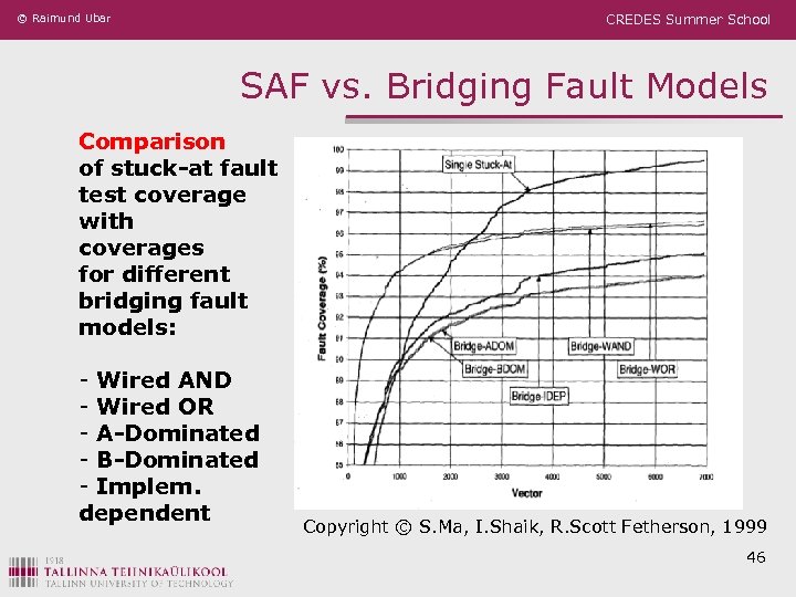
© Raimund Ubar CREDES Summer School SAF vs. Bridging Fault Models Comparison of stuck-at fault test coverage with coverages for different bridging fault models: - Wired AND - Wired OR - A-Dominated - B-Dominated - Implem. dependent Copyright © S. Ma, I. Shaik, R. Scott Fetherson, 1999 46
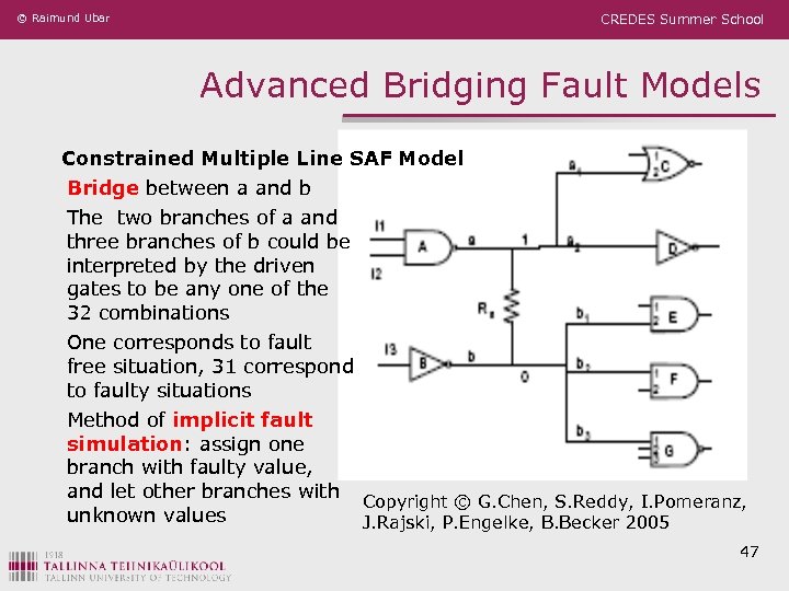
© Raimund Ubar CREDES Summer School Advanced Bridging Fault Models Constrained Multiple Line SAF Model Bridge between a and b The two branches of a and three branches of b could be interpreted by the driven gates to be any one of the 32 combinations One corresponds to fault free situation, 31 correspond to faulty situations Method of implicit fault simulation: assign one branch with faulty value, and let other branches with unknown values Copyright © G. Chen, S. Reddy, I. Pomeranz, J. Rajski, P. Engelke, B. Becker 2005 47

© Raimund Ubar CREDES Summer School Advanced Bridging Fault Models Constrained (conditional) Multiple Line SAF Model Advantages: ü Method is uniform to consider opens and bridges ü Method does not need circuit level information such as relative strengths and threshold voltages of transistors associated with bridge ü Method allows different levels of model complexity and accuracy (e. g. using implicit simulation with different number of unknown values) ü Method is based on constrained SAF model, hence, traditional gate level tools can be used 48
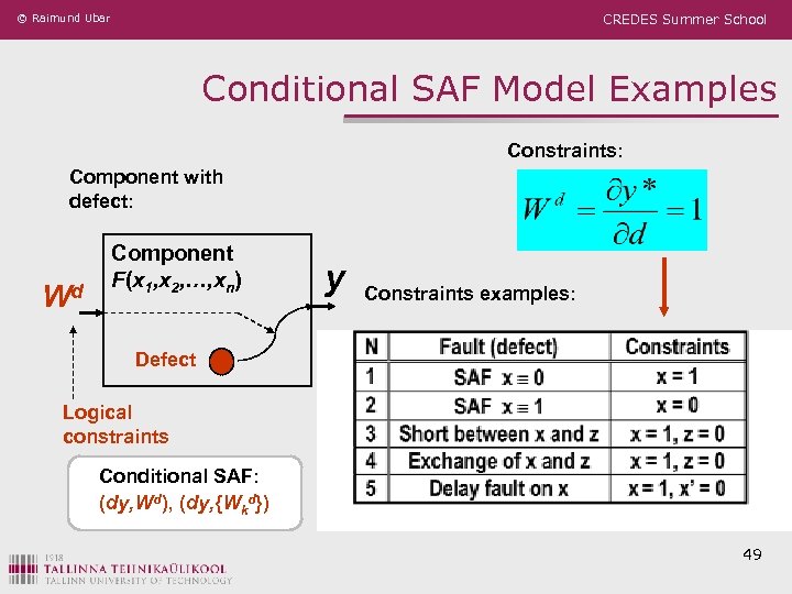
© Raimund Ubar CREDES Summer School Conditional SAF Model Examples Constraints: Component with defect: Wd Component F(x 1, x 2, …, xn) y Constraints examples: Defect Logical constraints Conditional SAF: (dy, Wd), (dy, {Wkd}) 49
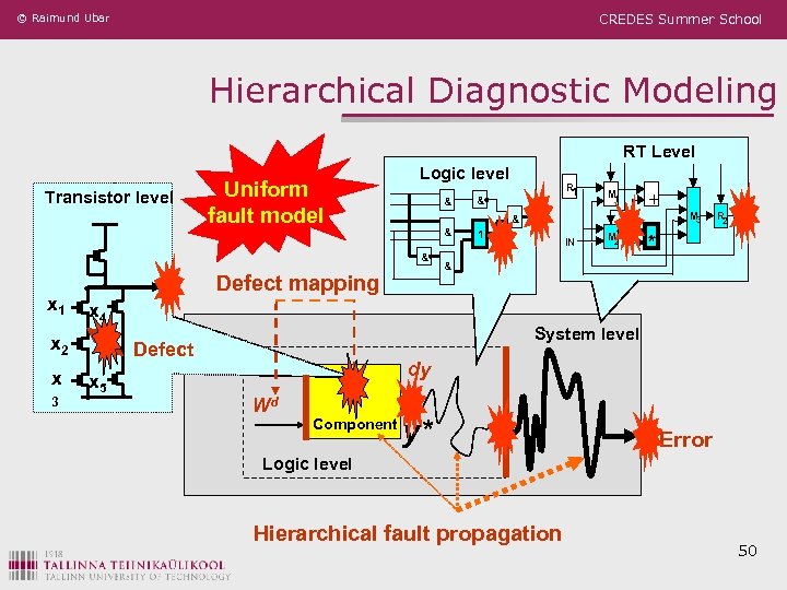
© Raimund Ubar CREDES Summer School Hierarchical Diagnostic Modeling RT Level Transistor level Uniform fault model Logic level & & Defect mapping x 4 x 2 x 3 + 1 IN M 2 M 3 R 2 * & System level Defect x 5 M 1 & & x 1 R 1 & dy Wd Component y* Error Logic level Hierarchical fault propagation 50
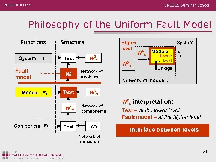
© Raimund Ubar CREDES Summer School Philosophy of the Uniform Fault Model Functions System: F Fault model Module Fk Structure Test F Wk Test Higher level WSk Network of modules WSk Module Lower level k Bridge Network of modules WSki WFki Component Fki W Fk System Network of components Test Wdki WFk interpretation: Test – at the lower level Fault model – at the higher level Interface between levels Network of transistors 51
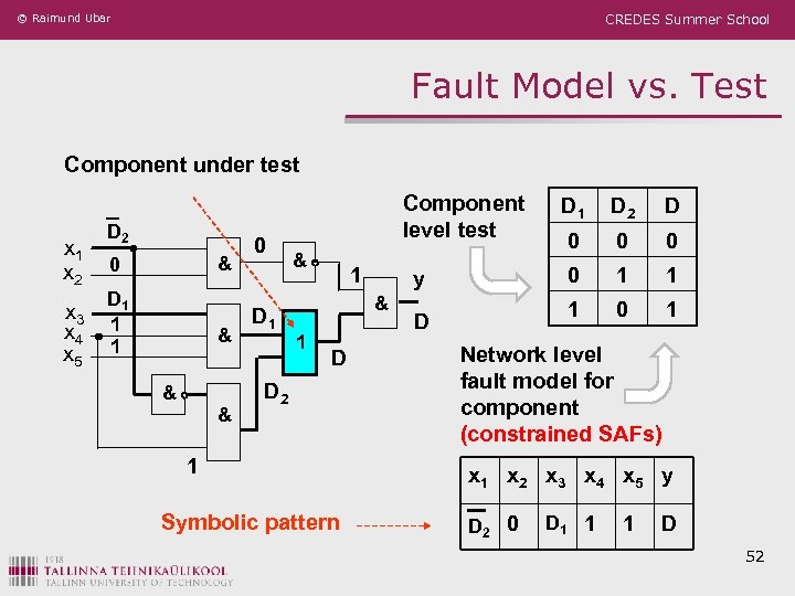
© Raimund Ubar CREDES Summer School Fault Model vs. Test Component under test x 1 x 2 x 3 x 4 x 5 D 2 & 0 D 1 1 1 & & & 0 D 1 Component level test & 1 D D 2 1 Symbolic pattern D 0 0 0 1 1 1 D D 2 0 y D 1 0 1 Network level fault model for a component (constrained SAFs) x 1 x 2 x 3 x 4 x 5 y D 2 0 D 1 1 1 D 52
© Raimund Ubar CREDES Summer School Motivations for High-Level Fault Models Current situation: • The efficiency of test generation (quality, speed) is highly depending on • the description method (level, language), and • fault models • Because of the growing complexity of systems, gate level methods have become obsolete • High-Level methods for diagnostic modeling are today emerging, however they are not still mature Main disadvantages: • The known methods for fault modeling are • dedicated to special classes (i. e. for microprocessors, for RTL, VHDL etc. languages. . . ), not general • not well defined and formalized 53
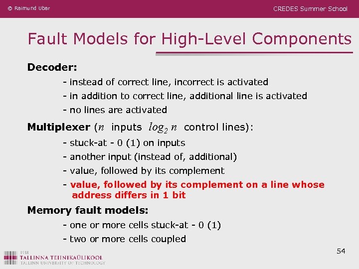
© Raimund Ubar CREDES Summer School Fault Models for High-Level Components Decoder: - instead of correct line, incorrect is activated - in addition to correct line, additional line is activated - no lines are activated Multiplexer (n inputs log 2 n control lines): - stuck-at - 0 (1) on inputs - another input (instead of, additional) - value, followed by its complement on a line whose address differs in 1 bit Memory fault models: - one or more cells stuck-at - 0 (1) - two or more cells coupled 54
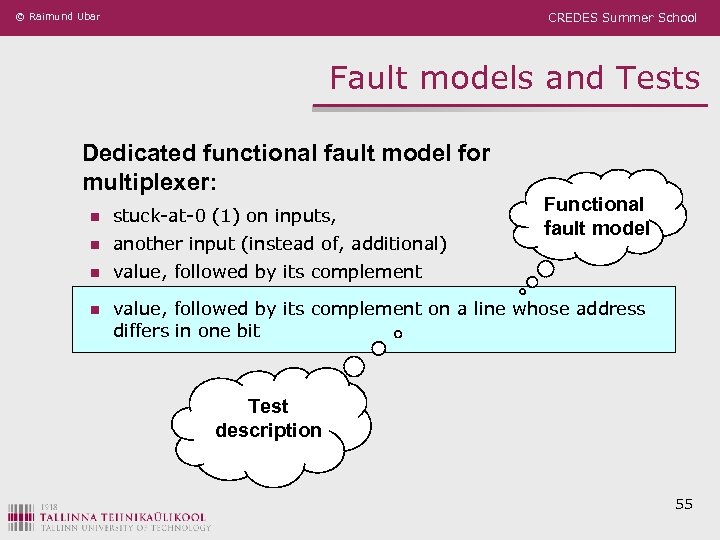
© Raimund Ubar CREDES Summer School Fault models and Tests Dedicated functional fault model for multiplexer: Functional fault model n stuck-at-0 (1) on inputs, n another input (instead of, additional) n value, followed by its complement on a line whose address differs in one bit Test description 55
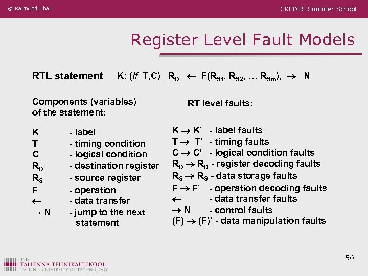
© Raimund Ubar CREDES Summer School Register Level Fault Models RTL statement K: (If T, C) RD F(RS 1, RS 2, … RSm), N Components (variables) of the statement: K T C RD RS F N - label - timing condition - logical condition - destination register - source register - operation - data transfer - jump to the next statement RT level faults: K K’ - label faults T T’ - timing faults C C’ - logical condition faults RD - register decoding faults RS - data storage faults F F’ - operation decoding faults - data transfer faults N - control faults (F)’ - data manipulation faults 56
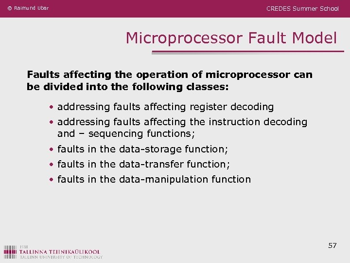
© Raimund Ubar CREDES Summer School Microprocessor Fault Model Faults affecting the operation of microprocessor can be divided into the following classes: • addressing faults affecting register decoding • addressing faults affecting the instruction decoding and – sequencing functions; • faults in the data-storage function; • faults in the data-transfer function; • faults in the data-manipulation function 57
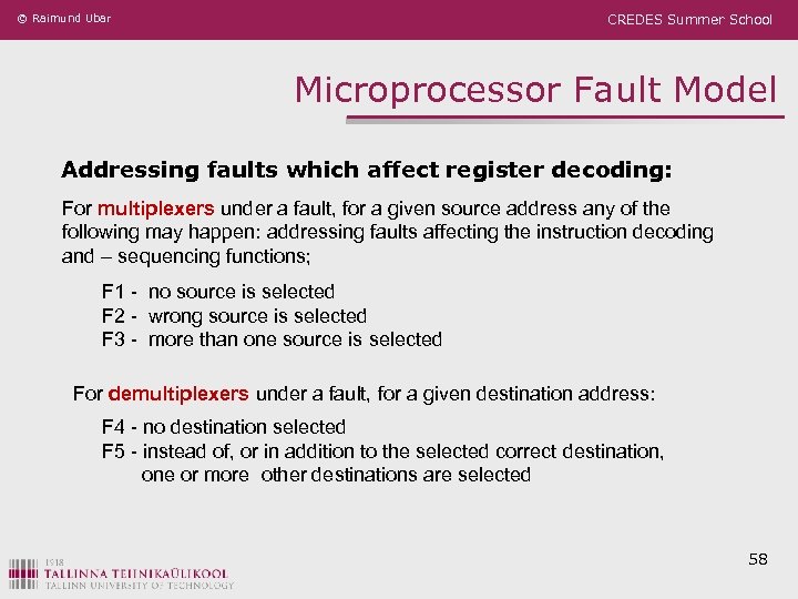
© Raimund Ubar CREDES Summer School Microprocessor Fault Model Addressing faults which affect register decoding: For multiplexers under a fault, for a given source address any of the following may happen: addressing faults affecting the instruction decoding and – sequencing functions; F 1 - no source is selected F 2 - wrong source is selected F 3 - more than one source is selected For demultiplexers under a fault, for a given destination address: F 4 - no destination selected F 5 - instead of, or in addition to the selected correct destination, one or more other destinations are selected 58
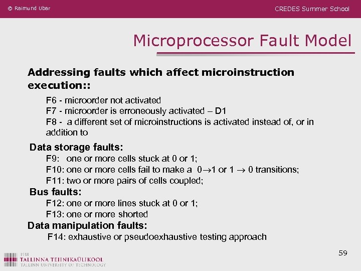
© Raimund Ubar CREDES Summer School Microprocessor Fault Model Addressing faults which affect microinstruction execution: : F 6 - microorder not activated F 7 - microorder is erroneously activated – D 1 F 8 - a different set of microinstructions is activated instead of, or in addition to Data storage faults: F 9: one or more cells stuck at 0 or 1; F 10: one or more cells fail to make a 0 1 or 1 0 transitions; F 11: two or more pairs of cells coupled; Bus faults: F 12: one or more lines stuck at 0 or 1; F 13: one or more shorted Data manipulation faults: F 14: exhaustive or pseudoexhaustive testing approach 59
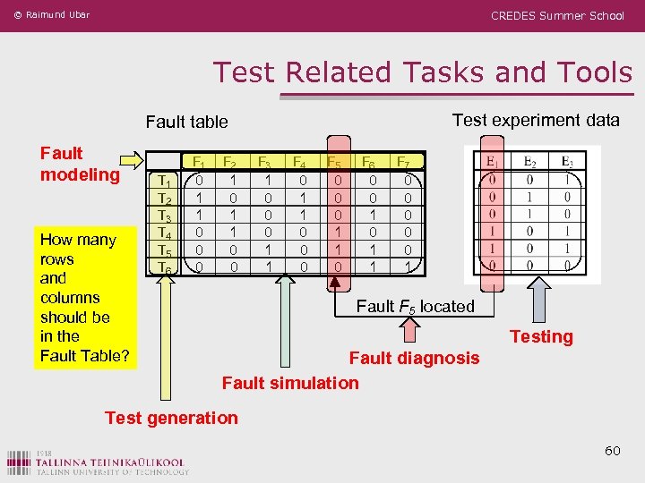
© Raimund Ubar CREDES Summer School Test Related Tasks and Tools Test experiment data Fault table Fault modeling How many rows and columns should be in the Fault Table? T 1 T 2 T 3 T 4 T 5 T 6 F 1 0 1 1 0 0 0 F 2 1 0 1 1 0 0 F 3 1 0 0 0 1 1 F 4 0 1 1 0 0 0 F 5 0 0 0 1 1 0 F 6 0 0 1 1 F 7 0 0 0 1 Fault F 5 located Testing Fault diagnosis Fault simulation Test generation 60
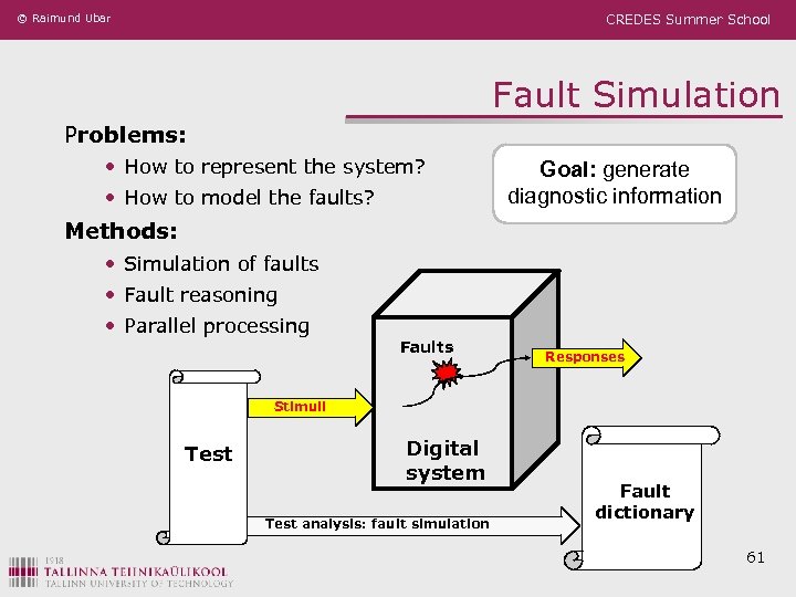
© Raimund Ubar CREDES Summer School Fault Simulation Problems: • How to represent the system? • How to model the faults? Goal: generate diagnostic information Methods: • Simulation of faults • Fault reasoning • Parallel processing Faults Responses Stimuli Test Digital system Test analysis: fault simulation Fault dictionary 61
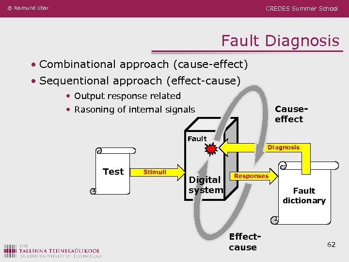
© Raimund Ubar CREDES Summer School Fault Diagnosis • Combinational approach (cause-effect) • Sequentional approach (effect-cause) • Output response related Causeeffect • Rasoning of internal signals Fault Diagnosis Test Stimuli Digital system Responses Fault dictionary Effectcause 62
© Raimund Ubar CREDES Summer School Fault diagnosis Fault Diagnosis methods ü Combinational methods n n ü The process of fault localization is carried out after finishing the whole testing experiment by combining all the gathered experimental data The diagnosis is made by using fault tables or fault dictionaries Sequential methods (adaptive testing) n ü The process of fault location is carried out step by step, where each step depends on the result of the diagnostic experiment at the previous step Sequential fault diagnosis can be carried out either n by observing only output responses of the UUT or n by pinpointing by a special probe also internal control points of the UUT (guided probing) 63
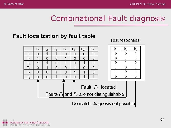
© Raimund Ubar CREDES Summer School Combinational Fault diagnosis Fault localization by fault table T 1 T 2 T 3 T 4 T 5 T 6 F 1 0 1 1 0 0 0 F 2 1 0 1 1 0 0 F 3 1 0 0 0 1 1 F 4 0 1 1 0 0 0 F 5 0 0 0 1 1 0 F 6 0 0 1 1 Test responses: F 7 0 0 0 1 Fault F 5 located Faults F 1 and F 4 are not distinguishable No match, diagnosis not possible 64
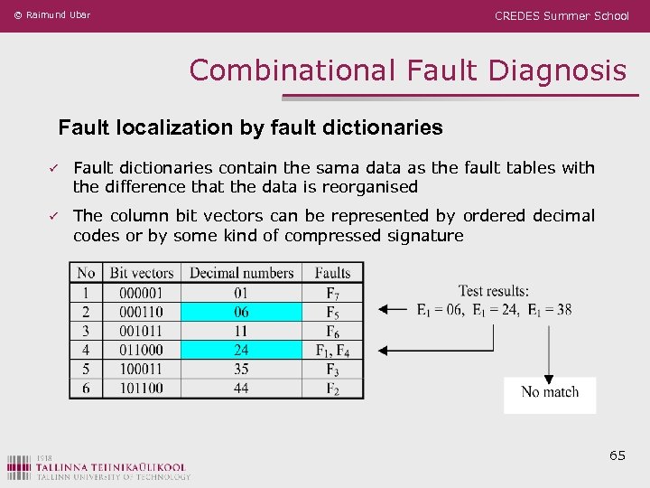
© Raimund Ubar CREDES Summer School Combinational Fault Diagnosis Fault localization by fault dictionaries ü Fault dictionaries contain the sama data as the fault tables with the difference that the data is reorganised ü The column bit vectors can be represented by ordered decimal codes or by some kind of compressed signature 65
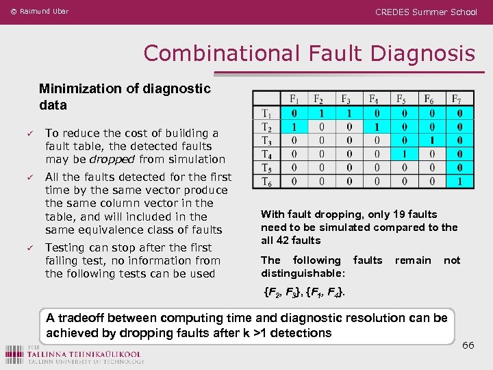
© Raimund Ubar CREDES Summer School Combinational Fault Diagnosis Minimization of diagnostic data ü To reduce the cost of building a fault table, the detected faults may be dropped from simulation ü All the faults detected for the first time by the same vector produce the same column vector in the table, and will included in the same equivalence class of faults ü Testing can stop after the first failing test, no information from the following tests can be used With fault dropping, only 19 faults need to be simulated compared to the all 42 faults The following faults distinguishable: remain not {F 2, F 3}, {F 1, F 4}. A tradeoff between computing time and diagnostic resolution can be achieved by dropping faults after k >1 detections 66
© Raimund Ubar CREDES Summer School Improving Diagnostic Resolution Generating tests to distinguish faults ü To improve the fault resolution of a given test set T, it is necessary to generate tests to distinguish among faults equivalent under T ü Consider the problem of distinguishing between faults F 1 and F 2. A test is to be found which detects one of these faults but not the other ü The following cases are possible: n F 1 and F 2 do not influence the same outputs • A test should be generated for F 1 (F 2) using only the circuit feeding the outputs influenced by F 1 (F 2) n F 1 and F 2 influence the same set of outputs. • A test should be generated for F 1 (F 2) without activating F 2 (F 1) ü How to activate a fault without activating another one? 67
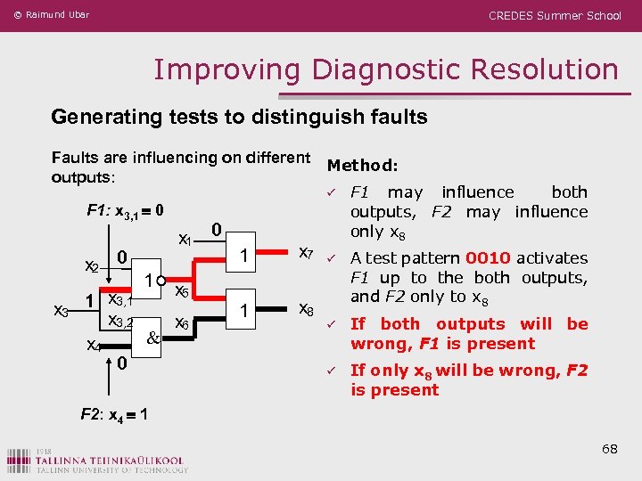
© Raimund Ubar CREDES Summer School Improving Diagnostic Resolution Generating tests to distinguish faults Faults are influencing on different Method: outputs: ü F 1 may influence both F 1: x 3, 1 0 outputs, F 2 may influence only x 8 x 0 x 2 0 x 3 1 1 x 7 1 x 8 ü A test pattern 0010 activates F 1 up to the both outputs, and F 2 only to x 8 ü If both outputs will be wrong, F 1 is present ü If only x 8 will be wrong, F 2 is present 1 x 5 x 3, 1 1 x 3, 2 x 6 & x 4 0 F 2: x 4 1 68
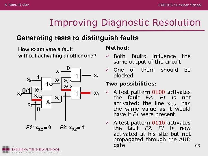
© Raimund Ubar CREDES Summer School Improving Diagnostic Resolution Generating tests to distinguish faults How to activate a fault without activating another one? x 2 1 1 x 3, 1 x 3 0/1 x 3, 2 & x 4 0 F 1: x 3, 2 0 x 1 0 1 x 5, 2 1 x 6 F 2: x 5, 2 1 x 7 Method: ü Both faults influence the same output of the circuit ü One of blocked them should be Two possibilities: x 8 ü A test pattern 0100 activates the fault F 2. F 1 is not activated: the line x 3, 2 has the same value as it would have if F 1 were present ü A test pattern 0110 activates the fault F 2. F 1 is now activated at his site but not propagated through the AND gate 69
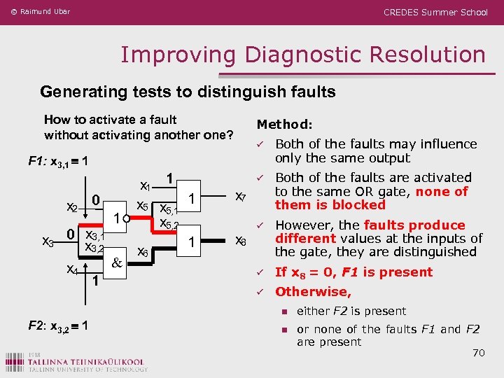
© Raimund Ubar CREDES Summer School Improving Diagnostic Resolution Generating tests to distinguish faults How to activate a fault without activating another one? F 1: x 3, 1 1 x 2 0 x 3, 1 x 3 0 x 3, 2 x 4 1 1 & x 1 1 x 5, 2 1 x 6 Method: ü Both of the faults may influence only the same output ü Both of the faults are activated to the same OR gate, none of them is blocked ü However, the faults produce different values at the inputs of the gate, they are distinguished ü If x 8 = 0, F 1 is present ü Otherwise, x 7 x 8 n F 2: x 3, 2 1 either F 2 is present n or none of the faults F 1 and F 2 are present 70
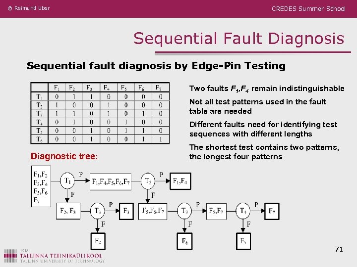
© Raimund Ubar CREDES Summer School Sequential Fault Diagnosis Sequential fault diagnosis by Edge-Pin Testing Two faults F 1, F 4 remain indistinguishable Not all test patterns used in the fault table are needed Different faults need for identifying test sequences with different lengths Diagnostic tree: The shortest contains two patterns, the longest four patterns 71
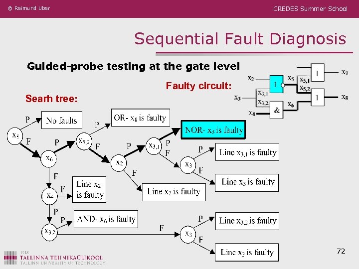
© Raimund Ubar CREDES Summer School Sequential Fault Diagnosis Guided-probe testing at the gate level Faulty circuit: Searh tree: 72
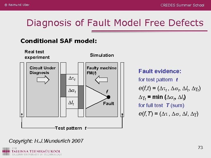
© Raimund Ubar CREDES Summer School Diagnosis of Fault Model Free Defects Conditional SAF model: Real test experiment Simulation Circuit Under Diagnosis t t lt Faulty machine FM(f) Fault evidence: for test pattern t f Fault e(f, t) = ( t , t, lt, t) t = min ( t, lt) for full test T (sum) e(f, T) = ( , , l, ) Test pattern t Copyright: H. J. Wunderlich 2007 73
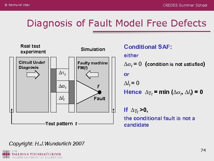
© Raimund Ubar CREDES Summer School Diagnosis of Fault Model Free Defects Real test experiment Circuit Under Diagnosis Simulation Conditional SAF: either t Faulty machine FM(f) t lt t = 0 (condition is not satisfied) or f Fault lt = 0 Hence t = min ( t, lt) = 0 If t >0, Test pattern t the conditional fault is not a candidate Copyright: H. J. Wunderlich 2007 74
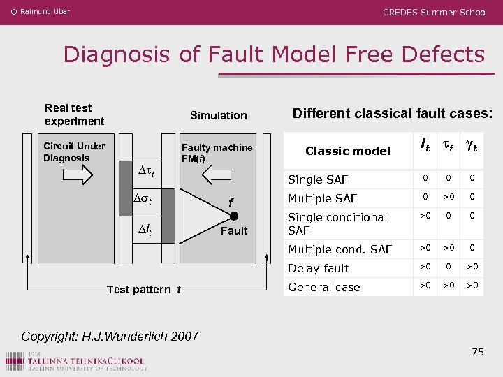
© Raimund Ubar CREDES Summer School Diagnosis of Fault Model Free Defects Real test experiment Simulation Circuit Under Diagnosis Faulty machine FM(f) t Different classical fault cases: Classic model l t t t Test pattern t Fault 0 0 Multiple SAF 0 >0 0 Single conditional SAF >0 0 0 >0 >0 0 Delay fault lt f 0 Multiple cond. SAF t Single SAF >0 0 >0 General case >0 >0 >0 Copyright: H. J. Wunderlich 2007 75
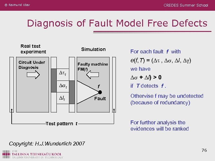
© Raimund Ubar CREDES Summer School Diagnosis of Fault Model Free Defects Real test experiment Circuit Under Diagnosis Simulation t Faulty machine FM(f) t lt Test pattern t For each fault f with e(f, T) = ( , , l, ) we have + l) > 0 f Fault if T detects f. Othervise f may be undetected (because of redundancy) For further analysis the evidences will be ranked Copyright: H. J. Wunderlich 2007 76
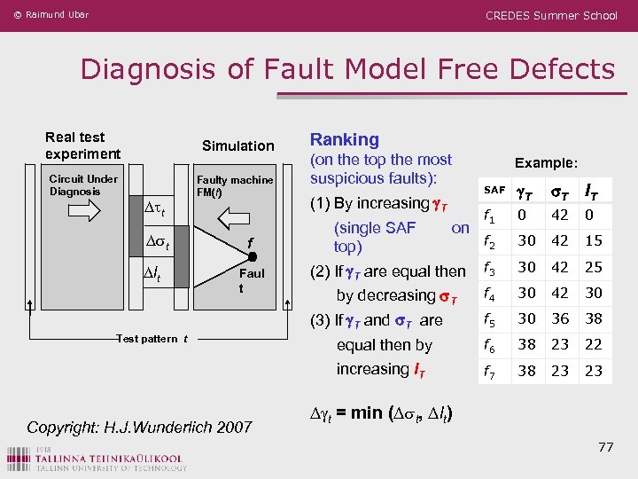
© Raimund Ubar CREDES Summer School Diagnosis of Fault Model Free Defects Real test experiment Simulation Circuit Under Diagnosis Faulty machine FM(f) t t lt f Faul t Test pattern t Copyright: H. J. Wunderlich 2007 Ranking (on the top the most suspicious faults): (1) By increasing T (single SAF on top) (2) If T are equal then by decreasing T (3) If T and T are equal then by increasing l. T Example: SAF T T l. T f 1 0 42 0 f 2 30 42 15 f 3 30 42 25 f 4 30 42 30 f 5 30 36 38 f 6 38 23 22 f 7 38 23 23 t = min ( t, lt) 77
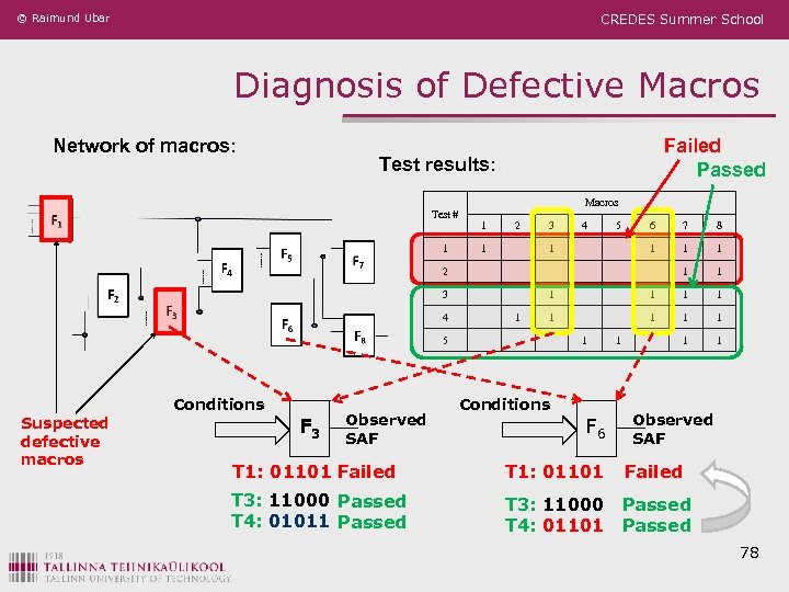
© Raimund Ubar CREDES Summer School Diagnosis of Defective Macros Network of macros: Failed Passed Test results: : Test # 1 Macros 1 2 4 5 7 8 1 1 6 1 1 3 1 2 3 4 1 1 1 5 Conditions Suspected defective macros F 3 Observed SAF 1 Conditions F 6 1 Observed SAF T 1: 01101 Failed T 3: 11000 Passed T 4: 01011 Passed T 3: 11000 Passed T 4: 01101 Passed 78
© Raimund Ubar CREDES Summer School Conclusions ü ü ü There is a huge number of fault models in use Low level SAF model is still de facto standard for test quality measuring by fault simulation Conditional SAF is a promising model for covering a large class of physical defects Fault model free diagnosis is a new promising approach for locating physical defects High-level fault models are good guides for highlevel test generation There is no difference between fault and test, it is only an interpretation issue www. pld. ttu. ee/~raiub/ 79

© Raimund Ubar CREDES Summer School For Additional Reading 1. 2. 3. 4. 5. 6. 7. L. -T. Wang, C. -W. Wu, X. Wen. VLSI Test Principles and Architectures. Elsevier, 2006. D. Gizopulos. Advances in Electronic Testing, Technology & Engineering. Springer, 2006. O. Novak, E. Gramatova, R. Ubar. Handbook of Testing Electronic Systems. Czech TU Publishing House, 2005. N. Jha, S. Gupta. Testing of Digital Systems. Cambridge Univ. Press, 2003. M. L. Bushnell, V. D. Agrawal. Essentials of Electronic Testing. Kluwer Academic Publishers, 2000. M. Sachdev. Defect Oriented Testing for CMOS Analog and Digital Circuits. Kluwer Academic Publishers, 1998. A. Kristic, K. -T. Cheng. Delay Fault Testing for VLSI Circuits. Kluwer Academic Publishers, 1998. 80
6d08b35c6c4fc9c753582d5259dd3c1b.ppt