b3a53449b1edbcf949e88733a8fbc700.ppt
- Количество слайдов: 28
 CPEN 315 - Digital System Design Chapter 9 – Computer Design C. Gerousis © Logic and Computer Design Fundamentals, 4 rd Ed. , Mano Prentice Hall Charles Kime & Thomas Kaminski © 2008 Pearson Education, Inc.
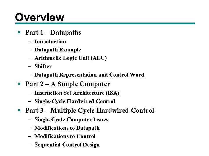 Overview § Part 1 – Datapaths – – – Introduction Datapath Example Arithmetic Logic Unit (ALU) Shifter Datapath Representation and Control Word § Part 2 – A Simple Computer – Instruction Set Architecture (ISA) – Single-Cycle Hardwired Control § Part 3 – Multiple Cycle Hardwired Control – – Single Cycle Computer Issues Modifications to Datapath Modifications to Control Sequential Control Design
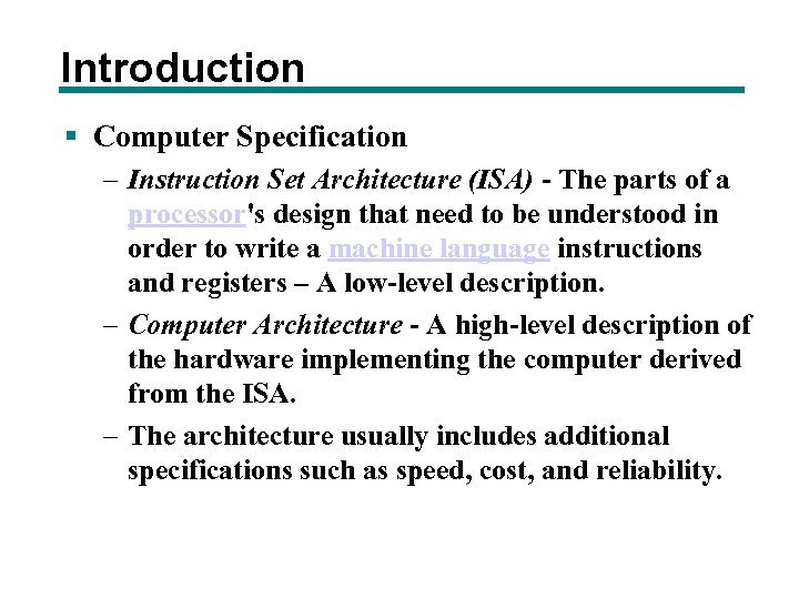 Introduction § Computer Specification – Instruction Set Architecture (ISA) - The parts of a processor's design that need to be understood in order to write a machine language instructions and registers – A low-level description. – Computer Architecture - A high-level description of the hardware implementing the computer derived from the ISA. – The architecture usually includes additional specifications such as speed, cost, and reliability.
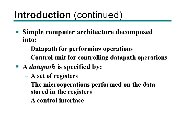 Introduction (continued) § Simple computer architecture decomposed into: – Datapath for performing operations – Control unit for controlling datapath operations § A datapath is specified by: – A set of registers – The microoperations performed on the data stored in the registers – A control interface
 Datapaths § Guiding principles for basic datapaths: – The set of registers § Collection of individual registers § A set of registers with common access resources called a register file § A combination of the above – Microoperation implementation One or more shared resources for implementing microoperations § Buses - shared transfer paths § Arithmetic-Logic Unit (ALU) - shared resource for implementing arithmetic and logic microoperations § Shifter - shared resource for implementing shift microoperations
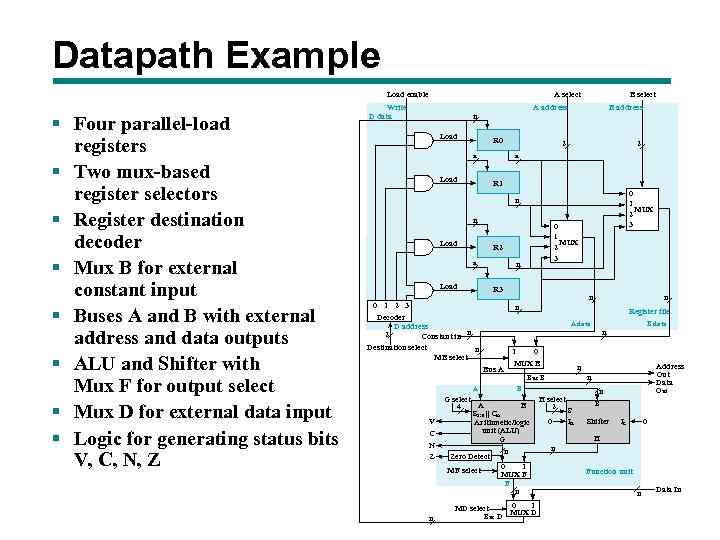 Datapath Example Load enable § Four parallel-load registers § Two mux-based register selectors § Register destination decoder § Mux B for external constant input § Buses A and B with external address and data outputs § ALU and Shifter with Mux F for output select § Mux D for external data input § Logic for generating status bits V, C, N, Z A select Write D data B select A address 2 n Load B address 2 R 0 n n Load R 1 0 1 MUX 2 3 n n 0 1 Load 2 3 R 2 n n Load MUX R 3 n 0 1 2 3 n n Decoder D address 2 Constant in n Destination select n MB select Register file A data 1 0 MUX B Bus A A n C N Z Zero Detect MF select n B G select A B 4 S 2: 0 || Cin Arithmetic/logic unit (ALU) G n 0 1 MUX F F n 0 1 MD select MUX D Bus D Address Out Data n Bus B V B data n H select 2 S IR 0 Out n B Shifter IL 0 H n Function unit n Data In
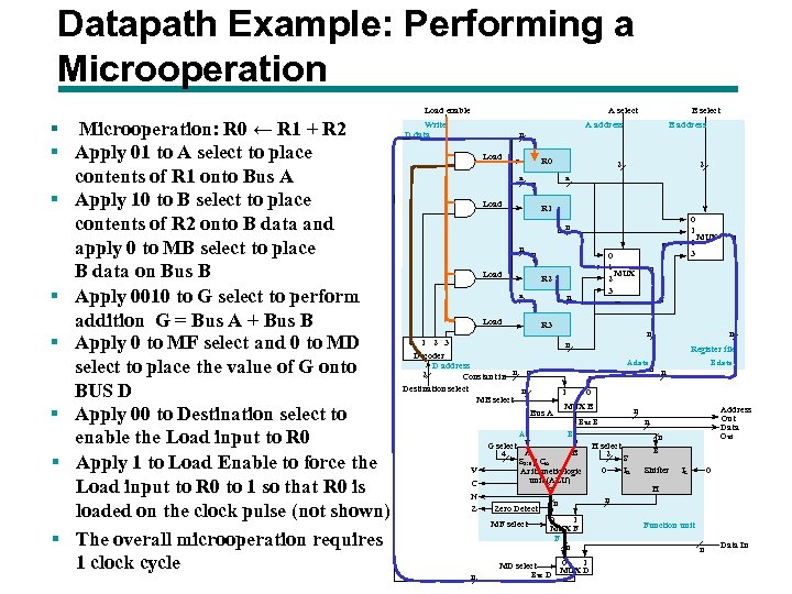 Datapath Example: Performing a Microoperation Load enable § Microoperation: R 0 ← R 1 + R 2 § Apply 01 to A select to place contents of R 1 onto Bus A § Apply 10 to B select to place contents of R 2 onto B data and apply 0 to MB select to place B data on Bus B § Apply 0010 to G select to perform addition G = Bus A + Bus B § Apply 0 to MF select and 0 to MD select to place the value of G onto BUS D § Apply 00 to Destination select to enable the Load input to R 0 § Apply 1 to Load Enable to force the Load input to R 0 to 1 so that R 0 is loaded on the clock pulse (not shown) § The overall microoperation requires 1 clock cycle A select Write D data B select A address Load B address 2 n 2 R 0 n n Load R 1 0 1 MUX 2 3 n n 0 1 Load 2 3 R 2 n n Load MUX R 3 n 0 1 2 3 n n Decoder D address 2 Constant in n Destination select n MB select Register file A data 1 0 MUX B Bus A A n C N Z B G select A B 4 S 2: 0 || Cin Arithmetic/logic unit (ALU) G 0 1 MUX F F n MF select MD select n Bus D H select 2 S IR 0 Out n B Shifter IL 0 H n n Zero Detect Address Out Data n Bus B V B data n 0 1 MUX D Function unit n Data In
 Arithmetic Logic Unit (ALU) § In this and the next section, we deal with design of typical ALUs and shifters § Decompose the ALU into: – An arithmetic circuit – A logic circuit – A selector to pick between the two circuits § Arithmetic circuit design – Decompose the arithmetic circuit into: § An n-bit parallel adder § A block of logic that selects four choices for the B input to the adder
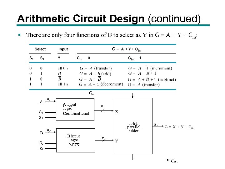 Arithmetic Circuit Design (continued) § There are only four functions of B to select as Y in G = A + Y + Cin: Cin A input logic Combinational S 0 S 1 B S 0 S 1 n X n-bit parallel adder n B input logic MUX n n Y Cout
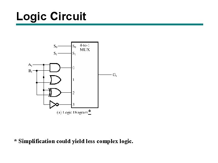 Logic Circuit * * Simplification could yield less complex logic.
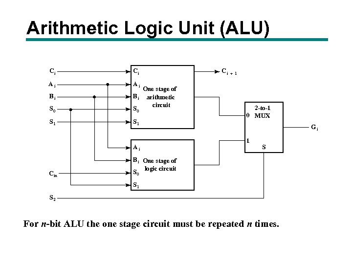 Arithmetic Logic Unit (ALU) Ci Ci Ai Ai S 0 One stage of B i arithmetic circuit S 0 S 1 Bi Ai C in Ci +1 2 -to-1 0 MUX Gi 1 S B i One stage of logic circuit S 0 S 1 S 2 For n-bit ALU the one stage circuit must be repeated n times.
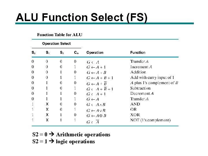
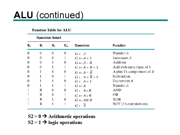 ALU (continued) S 2 = 0 Arithmetic operations S 2 = 1 logic operations
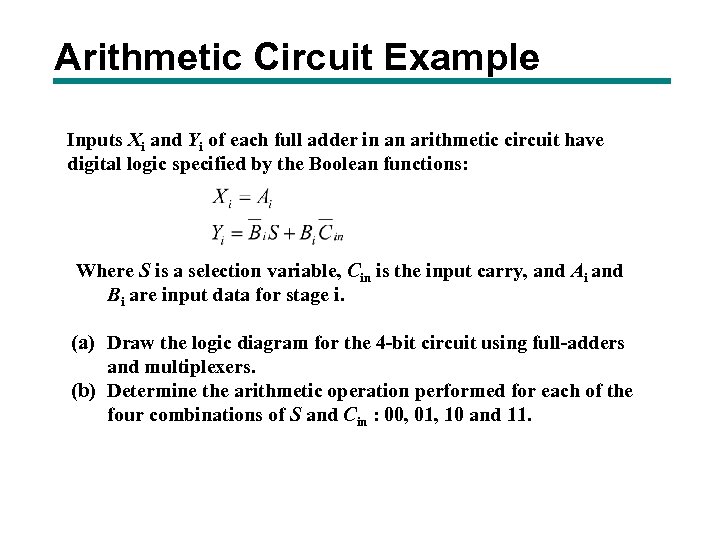 Arithmetic Circuit Example Inputs Xi and Yi of each full adder in an arithmetic circuit have digital logic specified by the Boolean functions: Where S is a selection variable, Cin is the input carry, and Ai and Bi are input data for stage i. (a) Draw the logic diagram for the 4 -bit circuit using full-adders and multiplexers. (b) Determine the arithmetic operation performed for each of the four combinations of S and Cin : 00, 01, 10 and 11.
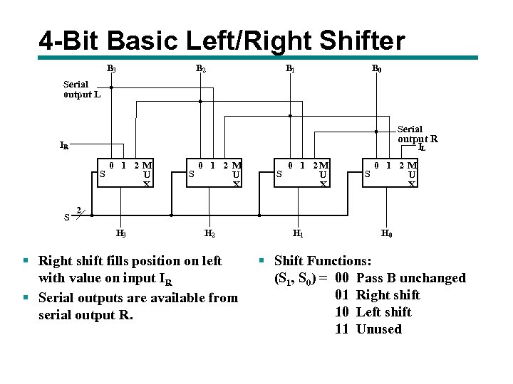 4 -Bit Basic Left/Right Shifter B 3 B 2 B 1 B 0 Serial output L Serial output R IL IR S S 0 1 2 M U X 2 H 3 H 2 § Right shift fills position on left with value on input IR § Serial outputs are available from serial output R. H 1 H 0 § Shift Functions: (S 1, S 0) = 00 Pass B unchanged 01 Right shift 10 Left shift 11 Unused
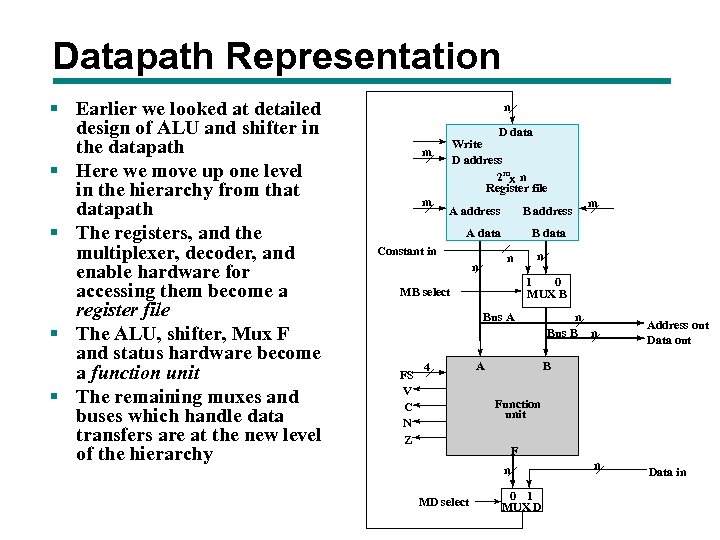 Datapath Representation § Earlier we looked at detailed design of ALU and shifter in the datapath § Here we move up one level in the hierarchy from that datapath § The registers, and the multiplexer, decoder, and enable hardware for accessing them become a register file § The ALU, shifter, Mux F and status hardware become a function unit § The remaining muxes and buses which handle data transfers are at the new level of the hierarchy n D data Write D address 2 mx n Register file m m A address B address A data Constant in B data n n n 1 0 MUX B MB select Bus A FS V C N Z 4 m A n Bus B n Address out Data out B Function unit F n MD select 0 1 MUX D n Data in
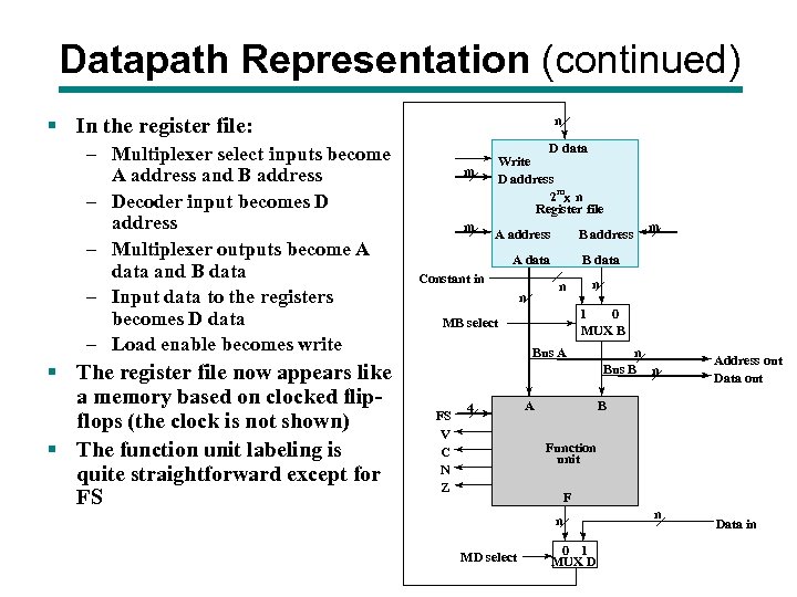 Datapath Representation (continued) n § In the register file: – Multiplexer select inputs become A address and B address – Decoder input becomes D address – Multiplexer outputs become A data and B data – Input data to the registers becomes D data – Load enable becomes write § The register file now appears like a memory based on clocked flipflops (the clock is not shown) § The function unit labeling is quite straightforward except for FS m m D data Write D address 2 mx n Register file A address B address A data Constant in B data n n n 1 0 MUX B MB select Bus A FS V C N Z 4 m A n Bus B n Address out Data out B Function unit F n MD select 0 1 MUX D n Data in
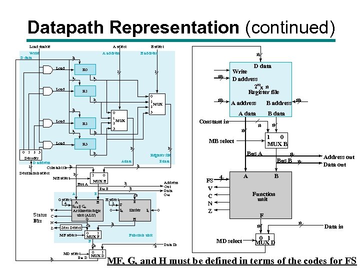 Datapath Representation (continued) Load enable A select Write D data B select A address 2 n Load 2 R 0 n R 1 0 1 MUX 2 3 n n 0 1 Load 2 3 R 2 n n Load B address A data n 1 0 MUX B n Bus A Register file B data n 1 0 MUX B n Bus B A B G select A B 4 S 2: 0 || Cin Arithmetic/logic unit (ALU) G 0 1 MUX F F n MF select MD select Bus D H select 2 S IR 0 Out n B Shifter IL 0 FS V C N Z 4 0 1 MUX D A B F H n Function unit n Data In Address out Data out Function unit n n Zero Detect Address Out Data n m B data n n n Bus A n A address MB select Decoder D address 2 Constant in n Destination select n MB select N Z D data Write D address 2 mx n Register file Constant in n C m MUX R 3 0 1 2 3 V m n Load Status Bits n B address MD select n Data in 0 1 MUX D MF, G, and H must be defined in terms of the codes for FS
 ALU Function Select (FS) S 2 = 0 Arithmetic operations S 2 = 1 logic operations
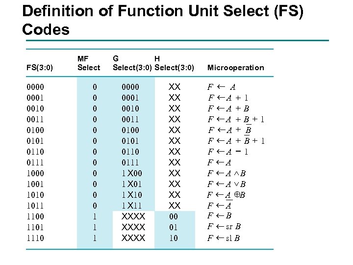 Definition of Function Unit Select (FS) G Select, H Select, and MF Codes of FS Codes in T FS(3: 0) 0000 0001 0010 0011 0100 0101 0110 0111 1000 1001 1010 1011 1100 1101 1110 MF Select 0 0 0 1 1 1 G H Select(3: 0) 0000 0001 0010 0011 0100 0101 0110 0111 1 X 00 1 X 01 1 X 10 1 X 11 XXXX XX XX XX 00 01 10 Microoperation F ¬ A F ¬A + 1 F ¬A + B + 1 F ¬A - 1 F ¬A F ¬ A ÙB F ¬ A ÚB F ¬ A ÅB F ¬A F ¬B F ¬ sr B F ¬ sl B
 The Control Word § The datapath has many control inputs § The signals driving these inputs can be defined and organized into a control word § To execute a microinstruction, we apply control word values for a clock cycle. For most microoperations, the positive edge of the clock cycle is needed to perform the register load § The datapath control word format and the field definitions are shown next
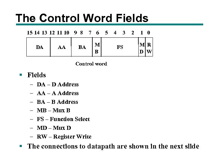 The Control Word Fields 15 14 13 12 11 10 9 8 DA AA 7 6 BA 5 M B 4 3 FS 2 1 0 MR D W Control word § Fields – – – – DA – D Address AA – A Address BA – B Address MB – Mux B FS – Function Select MD – Mux D RW – Register Write § The connections to datapath are shown in the next slide
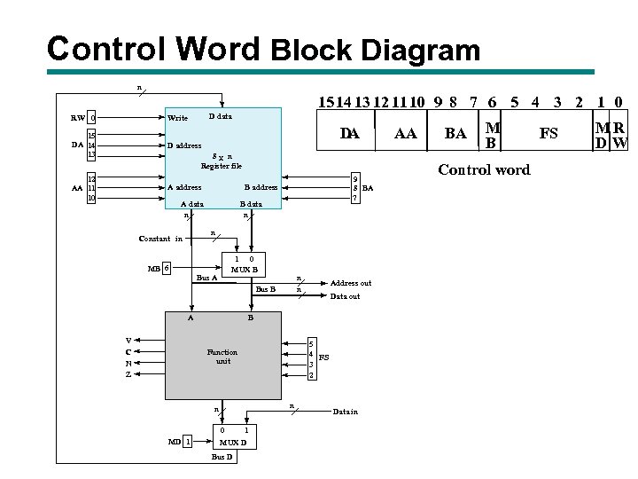 Control Word Block Diagram n 15 14 13 12 1110 9 8 7 6 5 4 3 2 1 0 RW 0 D data Write 15 DA 14 13 D A D address 8 x n Register file 12 AA 11 10 A address 9 8 BA 7 B address A data n B data n n Constant in MB 6 1 0 MUX B Bus A n n Bus B A V C N Z Data out B 5 4 FS 3 2 Function unit n n 0 MD 1 Address out 1 MUX D Bus D Data in AA BA M B Control word FS MR DW
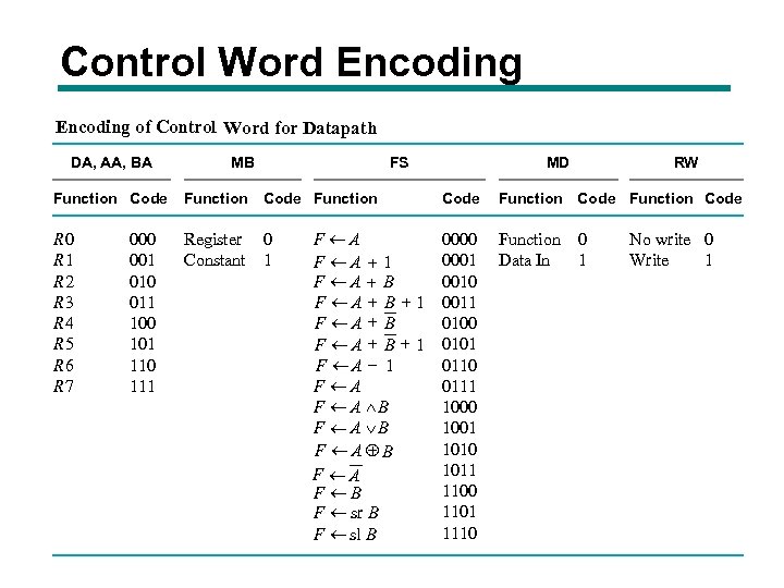 Control Word Encoding of Control Word for Datapath DA, AA, BA MB FS Function Code Function R 0 R 1 R 2 R 3 R 4 R 5 R 6 R 7 Register 0 Constant 1 000 001 010 011 100 101 110 111 MD Code F ¬A 0000 0001 F ¬A + 1 0010 F ¬A + B F ¬ A + B + 1 0011 F ¬A + B 0100 F ¬ A + B + 1 0101 F ¬A - 1 0110 F ¬A 0111 F ¬ A ÙB 1000 F ¬ A ÚB 1001 1010 F ¬A ÅB 1011 F ¬A 1100 F ¬B 1101 F ¬ sr B 1110 F ¬ sl B RW Function Code Function 0 Data In 1 No write 0 Write 1
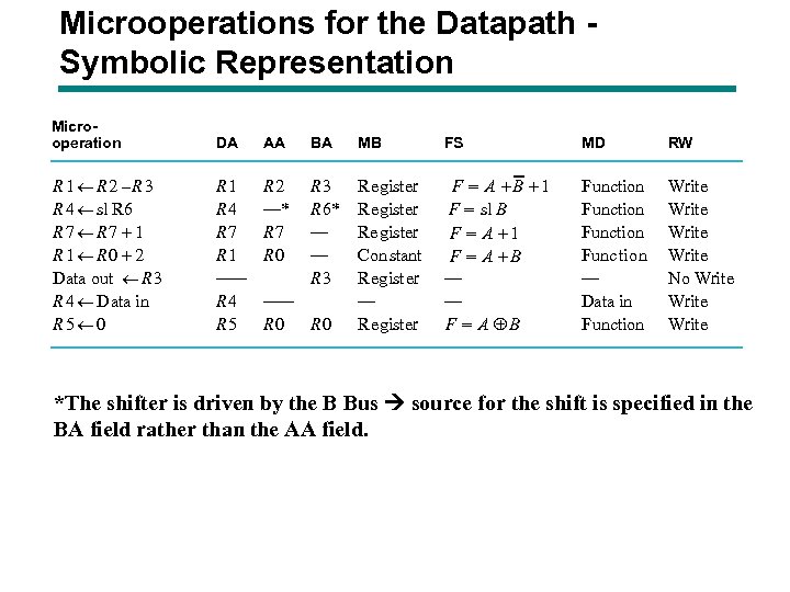 Microoperations for the Datapath Symbolic Representation Microoperation DA AA BA MB FS MD RW R 1¬R 2 –R 3 R 4 ¬ sl R 6 R 7¬R 7 + 1 R 1¬R 0 + 2 Data out ¬ R 3 R 4 ¬ Data in R 5¬ 0 R 1 R 4 R 7 R 1 —— R 4 R 5 R 2 —* R 7 R 0 R 3 R 6* — — R 3 Register Re gister Con stant Register — Register F = A +B +1 F = sl B F = A +1 F = A +B — — F = A ÅB Function Func tion — Data in Function Write No Write —— R 0 *The shifter is driven by the B Bus source for the shift is specified in the BA field rather than the AA field.
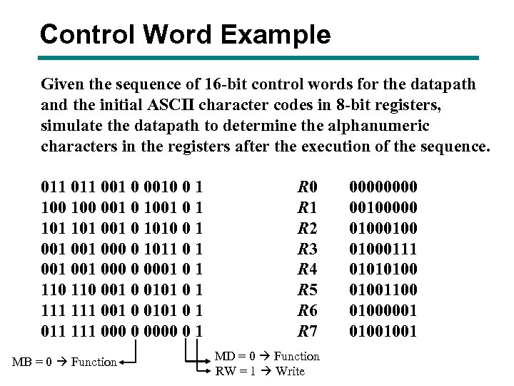 Control Word Example Given the sequence of 16 -bit control words for the datapath and the initial ASCII character codes in 8 -bit registers, simulate the datapath to determine the alphanumeric characters in the registers after the execution of the sequence. 011 001 0 0010 0 1 100 001 0 1 101 001 0 1010 0 1 001 000 0 1011 0 1 001 000 0 0001 0 1 110 001 0 0101 0 1 111 001 0 0101 0 1 011 111 000 0 0000 0 1 MB = 0 Function R 0 R 1 R 2 R 3 R 4 R 5 R 6 R 7 MD = 0 Function RW = 1 Write 0000 00100000 01000111 010101001100 01000001 01001001
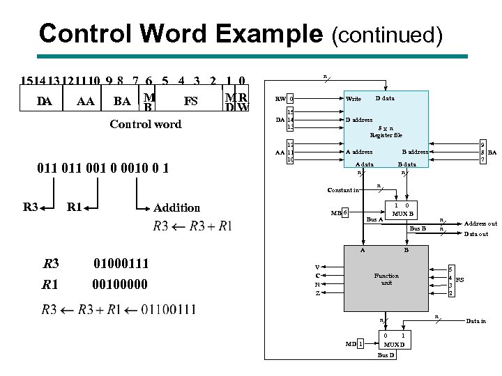 Control Word Example (continued) 1514 13121110 9 8 7 6 5 4 3 2 1 0 MR D A AA BA M FS B DW Control word 011 001 0 0010 0 1 n Write 15 DA 14 13 D address 12 AA 11 10 A address 8 x n Register file R 1 Addition 9 8 BA 7 B address A data n B data n n Constant in R 3 D data RW 0 MB 6 Bus A 1 0 MUX B n n Bus B A R 3 R 1 01000111 00100000 V C N Z Data out B 5 4 FS 3 2 Function unit n n MD 1 Address out 0 1 MUX D Bus D Data in
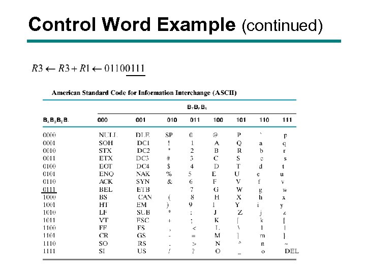 Control Word Example (continued)
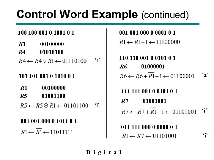 Control Word Example (continued) 100 001 0 1 R 1 R 4 001 000 0 0001 0 1 00100000 01010100 ‘t’ 110 001 0 0101 0 1 R 6 01000001 ‘a’ 101 001 0 1010 0 1 R 5 00100000 01001100 111 001 0 0101 0 1 R 7 ‘l’ 001 000 0 1011 0 1 01001001 ‘i’ 011 111 000 0 0000 0 1 ‘i’ D i g i t a l


