696159bb449cf3303bb9cf23209f8112.ppt
- Количество слайдов: 14
Computer Architecture Lecture 9 by Engineer A. Lecturer Aymen Hasan Al. Awady 10/2/2014 University of Kufa - Information Technology Research and Development Center 1 1
1. I/O Interfacing with 8085 • 8085 MPU separates memory from I/O, via software, ex: instructions like IN and, OUT for I/O interfacing and STA and LDA for memory. • When these instructions decoded by the processor it generates appropriate control signals IO/M. • MEMR and MEWR are control signals for Memory-mapped I/O and IOR and IOW for Peripheral Mapped I/O 2
2. IN Instruction. • IN instruction reads (copy) • • data from input devices like switches, keyboards and A/D data convertor. IN instruction is a two byte instruction with hexadecimal opcode DB, the second byte is the port address of an input device. This instruction reads the data from the input device and places it in the accumulator. 3
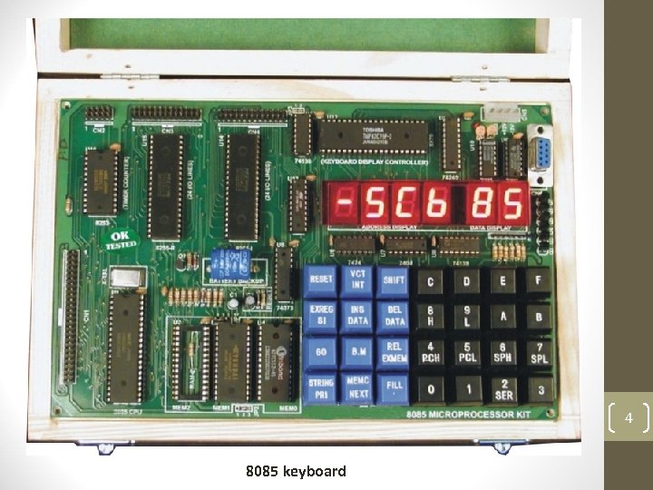
4 8085 keyboard
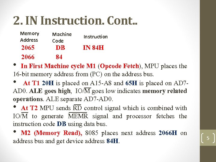
2. IN Instruction. Cont. . Memory Address Machine Code Instruction 2065 DB IN 84 H 2066 84 • In First Machine cycle M 1 (Opcode Fetch), MPU places the 16 -bit memory address from (PC) on the address bus. • At T 1 20 H is placed on A 15 -A 8 and 65 H is placed on AD 7 AD 0. ALE goes high, IO/M goes low indicates memory related operations. ALE separate AD 7 -AD 0. • At T 2 MPU sends RD control signal which is combined with IO/M to generate MEMR signal and processor fetches the instruction code DB using data bus. • M 2 (Memory Read), 8085 places next address 2066 H on address bus and get device address 84 H. 5
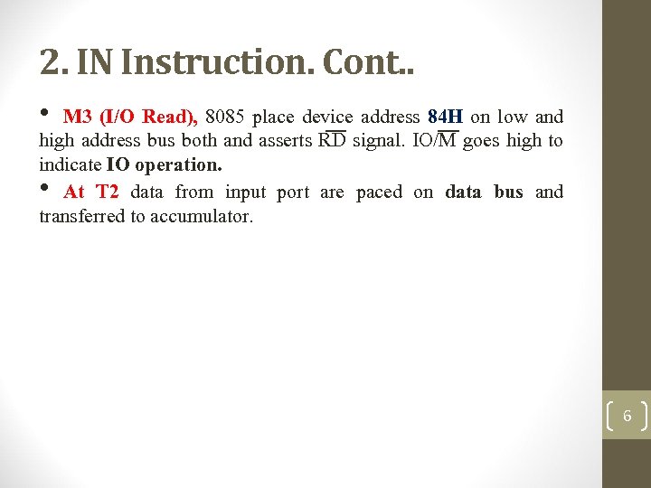
2. IN Instruction. Cont. . • M 3 (I/O Read), 8085 place device address 84 H on low and high address bus both and asserts RD signal. IO/M goes high to indicate IO operation. • At T 2 data from input port are paced on data bus and transferred to accumulator. 6
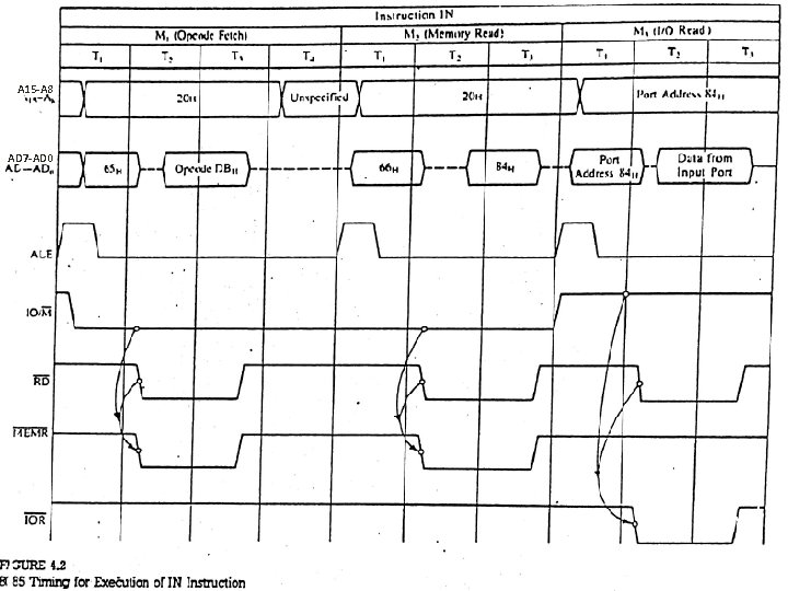
A 15 -A 8 AD 7 -AD 0 7
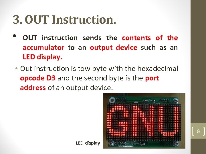
3. OUT Instruction. • OUT instruction sends the contents of the accumulator to an output device such as an LED display. • Out instruction is tow byte with the hexadecimal opcode D 3 and the second byte is the port address of an output device. 8 LED display
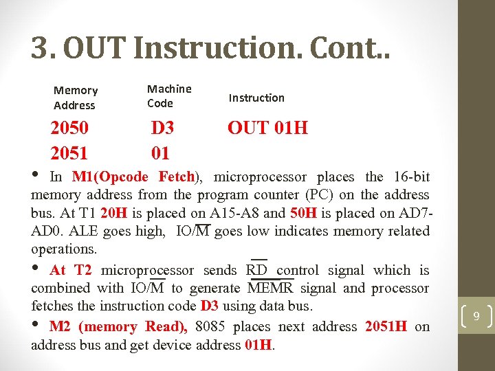
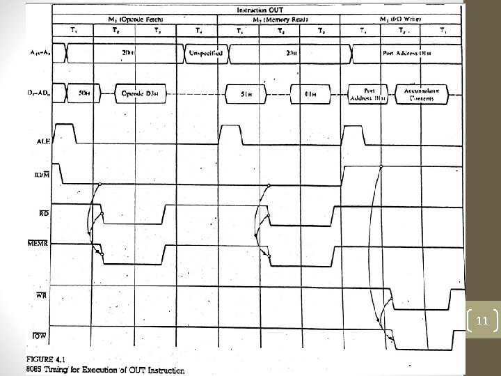
3. OUT Instruction. Cont. . Memory Address • 2050 2051 Machine Code D 3 01 Instruction OUT 01 H In M 1(Opcode Fetch), microprocessor places the 16 -bit memory address from the program counter (PC) on the address bus. At T 1 20 H is placed on A 15 -A 8 and 50 H is placed on AD 7 AD 0. ALE goes high, IO/M goes low indicates memory related operations. • At T 2 microprocessor sends RD control signal which is combined with IO/M to generate MEMR signal and processor fetches the instruction code D 3 using data bus. • M 2 (memory Read), 8085 places next address 2051 H on address bus and get device address 01 H. 9
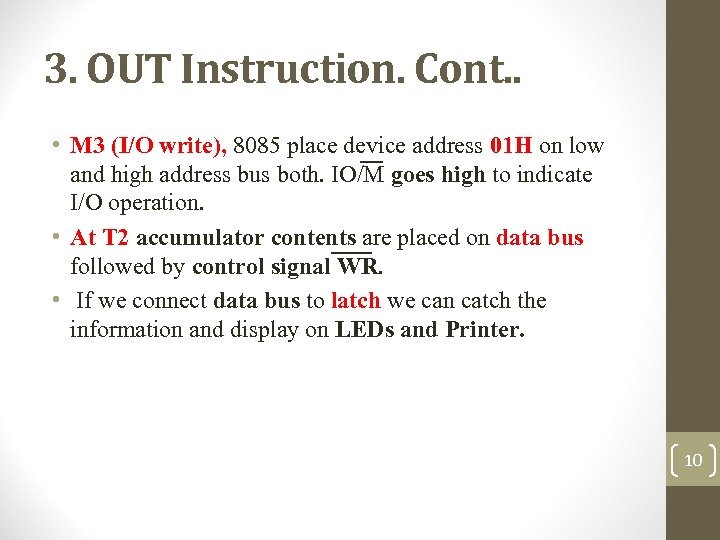
3. OUT Instruction. Cont. . • M 3 (I/O write), 8085 place device address 01 H on low and high address bus both. IO/M goes high to indicate I/O operation. • At T 2 accumulator contents are placed on data bus followed by control signal WR. • If we connect data bus to latch we can catch the information and display on LEDs and Printer. 10
11
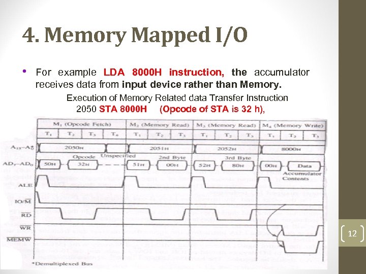
4. Memory Mapped I/O • For example LDA 8000 H instruction, the accumulator receives data from input device rather than Memory. Execution of Memory Related data Transfer Instruction 2050 STA 8000 H (Opcode of STA is 32 h), 12
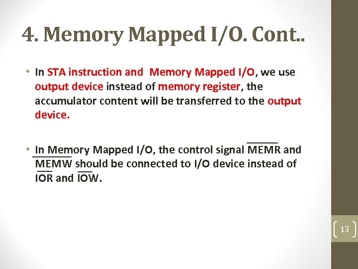
4. Memory Mapped I/O. Cont. . • In STA instruction and Memory Mapped I/O, we use output device instead of memory register, the accumulator content will be transferred to the output device. • In Memory Mapped I/O, the control signal MEMR and MEMW should be connected to I/O device instead of IOR and IOW. 13

End of lecture 9 14
696159bb449cf3303bb9cf23209f8112.ppt