9cb5572c3fcc98d1640487cf2f123fdf.ppt
- Количество слайдов: 20
 Comparison of a CCD and the Vanilla CMOS APS for Soft X-ray Diffraction Graeme Stewarta, R. Batesa, A. Bluea, A. Clarkc , S. Dhesib, D. Maneuskia, J. Marchalb, P. Steadmanb, N. Tartonib, R. Turchettac a: University of Glasgow, School of Physics and Astronomy, Kelvin Building, University Avenue, Glasgow, G 12 8 QQ b: Diamond Light Source Ltd, Diamond House, Harwell Science and Innovation Campus, Didcot, Oxfordshire, OX 11 0 DE c: STFC Rutherford Appleton Laboratory, Harwell Oxford, Didcot, OX 11 0 QX Graeme Stewart i. Wo. RID 13 6/7/11
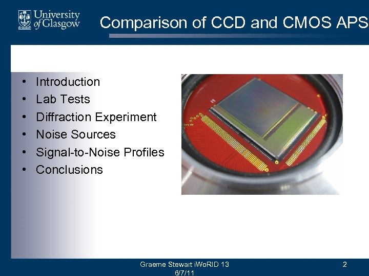 Comparison of CCD and CMOS APS • • • Introduction Lab Tests Diffraction Experiment Noise Sources Signal-to-Noise Profiles Conclusions Graeme Stewart i. Wo. RID 13 6/7/11 2
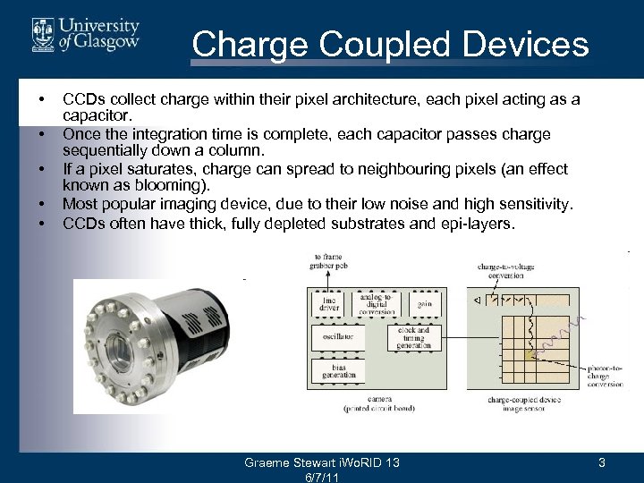 Charge Coupled Devices • • • CCDs collect charge within their pixel architecture, each pixel acting as a capacitor. Once the integration time is complete, each capacitor passes charge sequentially down a column. If a pixel saturates, charge can spread to neighbouring pixels (an effect known as blooming). Most popular imaging device, due to their low noise and high sensitivity. CCDs often have thick, fully depleted substrates and epi-layers. Graeme Stewart i. Wo. RID 13 6/7/11 3
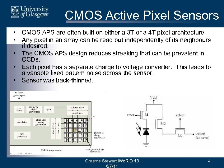 CMOS Active Pixel Sensors • CMOS APS are often built on either a 3 T or a 4 T pixel architecture. • Any pixel in an array can be read out independently of its neighbours if desired. • The CMOS APS design reduces streaking that can be prevalent in CCDs. • Each pixel has a separate charge to voltage converter. This leads to a variable fixed pattern noise across the sensor. • Sensor was back-thinned. Graeme Stewart i. Wo. RID 13 6/7/11 4
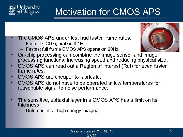 Motivation for CMOS APS • The CMOS APS under test had faster frame rates. – Fastest CCD operation 0. 1 Hz – Fastest full frame CMOS APS operation 20 Hz • On-chip processing can combine the image sensor and image processing functions, increasing speed and reducing physical size. • CMOS APS can read out a Region of Interest (Ro. I) for even faster frame rates. • CMOS APS are cheaper to fabricate. • CMOS APS do not have to be operated at low temperatures for reasonable signal to noise performance. • The sensitive, epitaxial layer in a CMOS APS has a limit on its thickness. – Detrimental for high energy imaging. Graeme Stewart i. Wo. RID 13 6/7/11 5
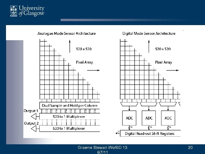
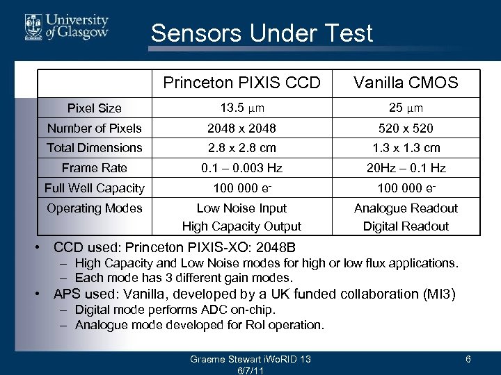 Sensors Under Test Princeton PIXIS CCD Vanilla CMOS Pixel Size 13. 5 μm 25 μm Number of Pixels 2048 x 2048 520 x 520 Total Dimensions 2. 8 x 2. 8 cm 1. 3 x 1. 3 cm Frame Rate 0. 1 – 0. 003 Hz 20 Hz – 0. 1 Hz Full Well Capacity 100 000 e- Operating Modes Low Noise Input High Capacity Output Analogue Readout Digital Readout • CCD used: Princeton PIXIS-XO: 2048 B – High Capacity and Low Noise modes for high or low flux applications. – Each mode has 3 different gain modes. • APS used: Vanilla, developed by a UK funded collaboration (MI 3) – Digital mode performs ADC on-chip. – Analogue mode developed for Ro. I operation. Graeme Stewart i. Wo. RID 13 6/7/11 6
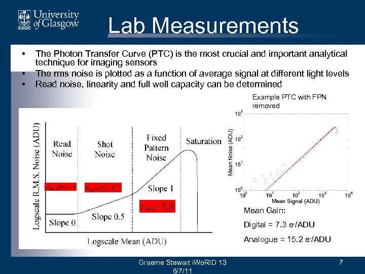 Lab Measurements • • • The Photon Transfer Curve (PTC) is the most crucial and important analytical technique for imaging sensors The rms noise is plotted as a function of average signal at different light levels Read noise, linearity and full well capacity can be determined Example PTC with FPN removed Mean Gain: Digital = 7. 3 e-/ADU Analogue = 15. 2 e-/ADU Graeme Stewart i. Wo. RID 13 6/7/11 7
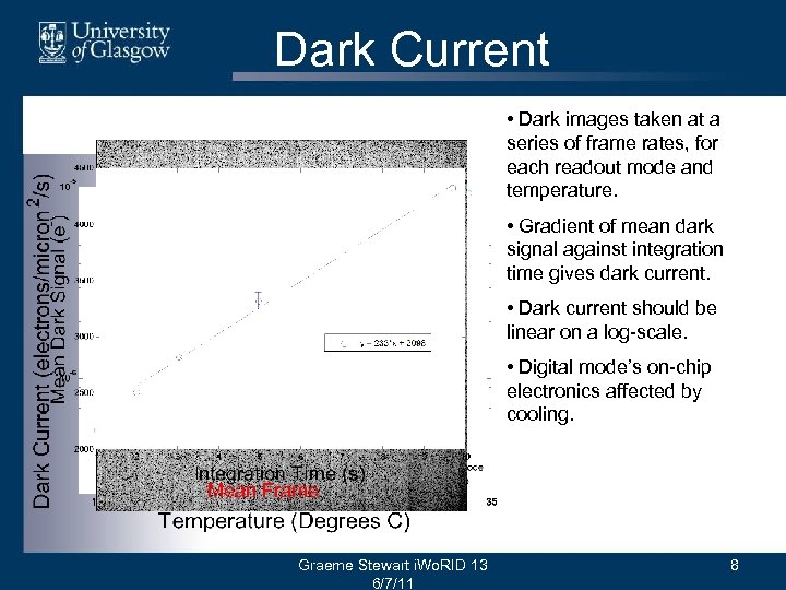 Dark Current • Dark images taken at a series of frame rates, for each readout mode and temperature. • Gradient of mean dark signal against integration time gives dark current. • Dark current should be linear on a log-scale. • Digital mode’s on-chip electronics affected by cooling. Mean Frame Graeme Stewart i. Wo. RID 13 6/7/11 8
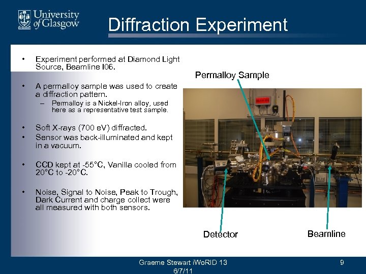 Diffraction Experiment • • Experiment performed at Diamond Light Source, Beamline I 06. Permalloy Sample A permalloy sample was used to create a diffraction pattern. – Permalloy is a Nickel-Iron alloy, used here as a representative test sample. • • Soft X-rays (700 e. V) diffracted. Sensor was back-illuminated and kept in a vacuum. • CCD kept at -55°C, Vanilla cooled from 20°C to -20°C. • Noise, Signal to Noise, Peak to Trough, Dark Current and charge collect were all measured with both sensors. Detector Graeme Stewart i. Wo. RID 13 6/7/11 Beamline 9
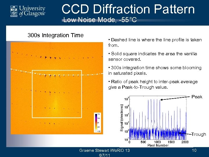 CCD Diffraction Pattern Low Noise Mode, -55°C 300 s Integration Time • Dashed line is where the line profile is taken from. • Solid square indicates the area the vanilla sensor covered. • 300 s integration time shows some blooming in saturated pixels. • Ratio of peak height to inter-peak average give a Peak-to-Trough value. Peak Trough Graeme Stewart i. Wo. RID 13 6/7/11 10
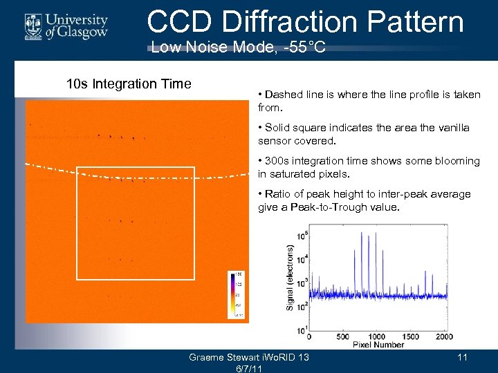 CCD Diffraction Pattern Low Noise Mode, -55°C 10 s Integration Time • Dashed line is where the line profile is taken from. • Solid square indicates the area the vanilla sensor covered. • 300 s integration time shows some blooming in saturated pixels. • Ratio of peak height to inter-peak average give a Peak-to-Trough value. Graeme Stewart i. Wo. RID 13 6/7/11 11
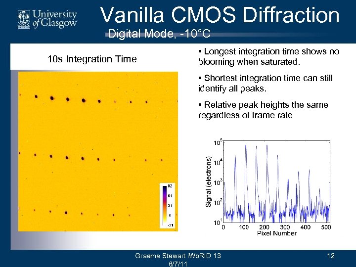 Vanilla CMOS Diffraction Digital Mode, -10°C 10 s Integration Time • Longest integration time shows no blooming when saturated. • Shortest integration time can still identify all peaks. • Relative peak heights the same regardless of frame rate Graeme Stewart i. Wo. RID 13 6/7/11 12
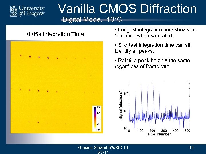 Vanilla CMOS Diffraction Digital Mode, -10°C 0. 05 s Integration Time • Longest integration time shows no blooming when saturated. • Shortest integration time can still identify all peaks. • Relative peak heights the same regardless of frame rate Graeme Stewart i. Wo. RID 13 6/7/11 13
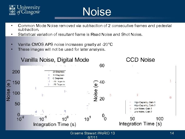 Noise • • Common Mode Noise removed via subtraction of 2 consecutive frames and pedestal subtraction. Statistical variation of resultant frame is Read Noise and Shot Noise. • • Vanilla CMOS APS noise increases greatly at -20°C These images will not be used for later analysis. Graeme Stewart i. Wo. RID 13 6/7/11 14
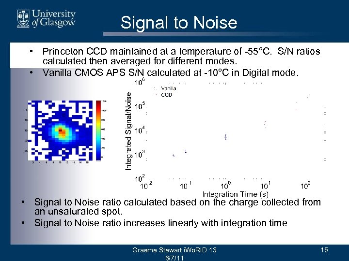 Signal to Noise • Princeton CCD maintained at a temperature of -55°C. S/N ratios calculated then averaged for different modes. • Vanilla CMOS APS S/N calculated at -10°C in Digital mode. • Signal to Noise ratio calculated based on the charge collected from an unsaturated spot. • Signal to Noise ratio increases linearly with integration time Graeme Stewart i. Wo. RID 13 6/7/11 15
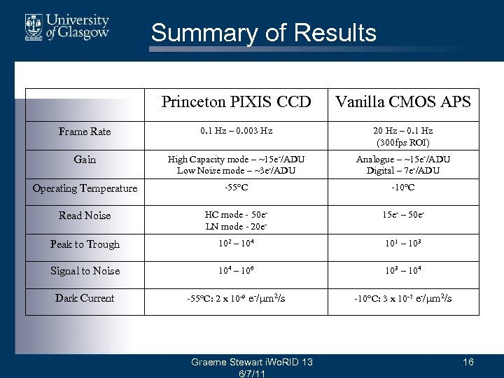 Summary of Results Princeton PIXIS CCD Vanilla CMOS APS Frame Rate 0. 1 Hz – 0. 003 Hz 20 Hz – 0. 1 Hz (300 fps ROI) Gain High Capacity mode – ~15 e-/ADU Low Noise mode – ~3 e-/ADU Analogue – ~15 e-/ADU Digital – 7 e-/ADU Operating Temperature -55°C -10°C Read Noise HC mode - 50 e. LN mode - 20 e- 15 e- – 50 e- Peak to Trough 102 – 104 101 – 103 Signal to Noise 104 – 106 103 – 104 Dark Current -55°C: 2 x 10 -9 e-/μm 2/s -10°C: 3 x 10 -7 e-/μm 2/s Graeme Stewart i. Wo. RID 13 6/7/11 16
 Conclusions • Vanilla CMOS detector, at -10°C, showed comparable noise performance to the Princeton CCD. – Maximum noise of 50 e- for both CCD and Vanilla CMOS APS • Charge collected increases linearly with integration time. • Further research remains to be completed on characterising the Region of Interest, as well as Spectral Response and Quantum Efficiency for the Vanilla CMOS. • Future CMOS APS could have k. Hz frame rates with a comparable S/N. Graeme Stewart i. Wo. RID 13 6/7/11 17
 Graeme Stewart i. Wo. RID 13 6/7/11 18
 Backups Graeme Stewart i. Wo. RID 13 6/7/11 19
 Graeme Stewart i. Wo. RID 13 6/7/11 20


