c150beb62d6520f86bc0311380c3b394.ppt
- Количество слайдов: 34
Comp. E 460 Real-Time and Embedded Systems Lecture 5 – Hardware Fundamentals
Click to edit Master title style Agenda • Prayer/Thoughts • Team Presentation - Brandon • Some Hardware Fundamentals • • • Open Collector outputs Tri-state outputs Signal Overloading Circuit Timing Parameters Buses • Address Maps • Attaching multiple things on a bus – Wait states – Wait Signals – No Handshake • • PAL’s/FPGA’s Watchdog Timer
Click Team Presentation style to edit Master title • Schematics
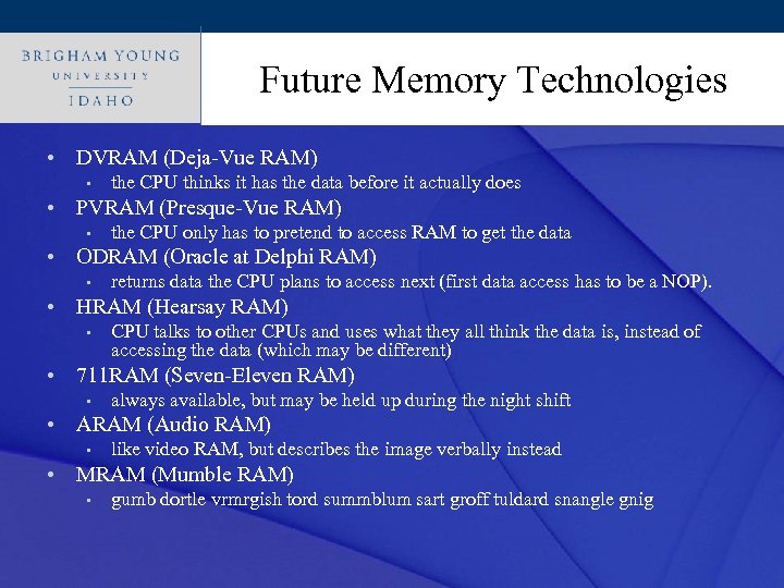
Futureto edit Master title style Click Memory Technologies • DVRAM (Deja-Vue RAM) • the CPU thinks it has the data before it actually does • PVRAM (Presque-Vue RAM) • the CPU only has to pretend to access RAM to get the data • ODRAM (Oracle at Delphi RAM) • returns data the CPU plans to access next (first data access has to be a NOP). • HRAM (Hearsay RAM) • CPU talks to other CPUs and uses what they all think the data is, instead of accessing the data (which may be different) • 711 RAM (Seven-Eleven RAM) • always available, but may be held up during the night shift • ARAM (Audio RAM) • like video RAM, but describes the image verbally instead • MRAM (Mumble RAM) • gumb dortle vrmrgish tord summblum sart groff tuldard snangle gnig
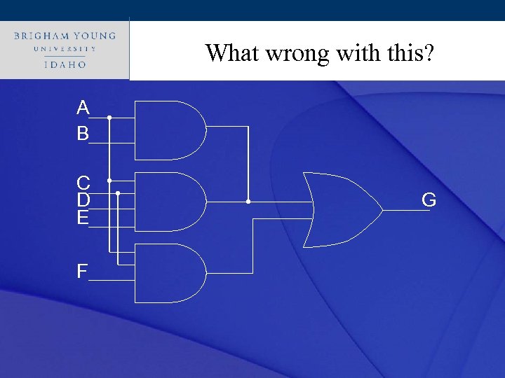
Click to edit Master title style What wrong with this? A B C D E F G
Click to edit Systems PC Master title style • What is an interrupt (in computer terms)? • On PC Systems, what are some sources of interrupts? • • USB Keyboard Disk Drive Mouse Network Card Graphics Card etc • Now, a big dilemma. On many processors, there is only one low asserted interrupt pin. A • How can we hook up multiple interrupts to this one pin? B C D E F G
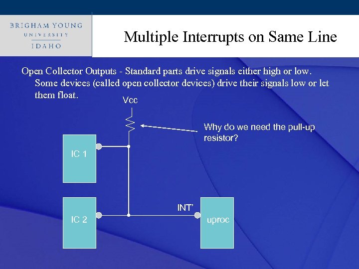
Multiple Interrupts on Same Line Click to edit Master title style Open Collector Outputs - Standard parts drive signals either high or low. Some devices (called open collector devices) drive their signals low or let them float. Vcc Why do we need the pull-up resistor? IC 1 INT’ IC 2 uproc
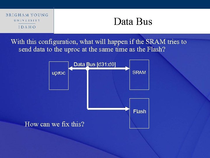
Click to edit Master title style Data Bus With this configuration, what will happen if the SRAM tries to send data to the uproc at the same time as the Flash? Data Bus [d 31: d 0] uproc SRAM Flash How can we fix this?
Click to edit Master title style Tri-State Outputs • Standard parts drive signals either high or low. • Open collector devices drive their signals low or let them float. • Tri-State devices can drive output high, low, or let them float. • Used when you want more than one device to drive an input • The outputs are enabled when the CS lines are true • Sometimes need pullup/down resistor on tristate lines – Why? • Figure 2. 16 in text
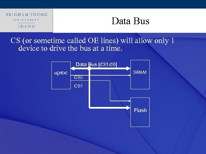
Click to edit Master title style Data Bus CS (or sometime called OE lines) will allow only 1 device to drive the bus at a time. Data Bus [d 31: d 0] uproc SRAM CS 0 CS 1 Flash
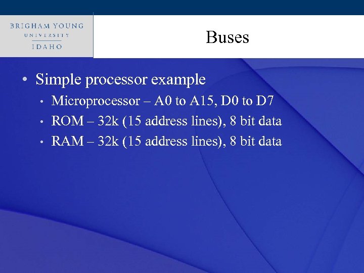
Click to edit Master title style Buses • Simple processor example • • • Microprocessor – A 0 to A 15, D 0 to D 7 ROM – 32 k (15 address lines), 8 bit data RAM – 32 k (15 address lines), 8 bit data
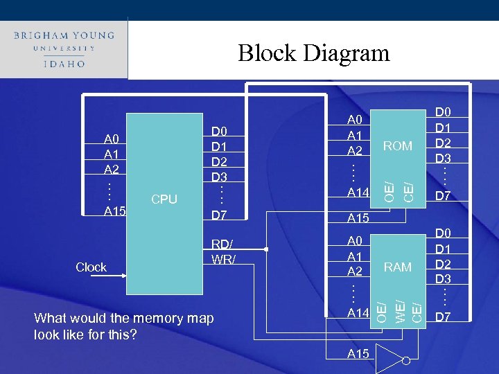
Click to edit Master title style Block Diagram Clock RD/ WR/ What would the memory map look like for this? CE/ ROM OE/ CPU D 0 D 1 D 2 D 3 : : D 7 A 15 A 0 A 1 A 2 : : A 14 A 15 RAM OE/ WE/ CE/ A 0 A 1 A 2 : : A 15 A 0 A 1 A 2 : : A 14 D 0 D 1 D 2 D 3 : : D 7
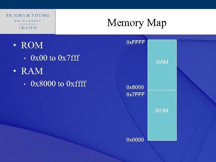
Click to Memory Map style edit Master title • ROM • 0 x. FFFF 0 x 00 to 0 x 7 fff RAM • RAM • 0 x 8000 to 0 xffff 0 x 8000 0 x 7 FFF ROM 0 x 0000
Click to edit other devices? ? ? How about Master title style • What about attaching keyboards, LCD’s, network chips, etc. • • How can we attach these types of devices to the microprocessor? What types of IO are available? Memory Mapped IO Isolated I/O space
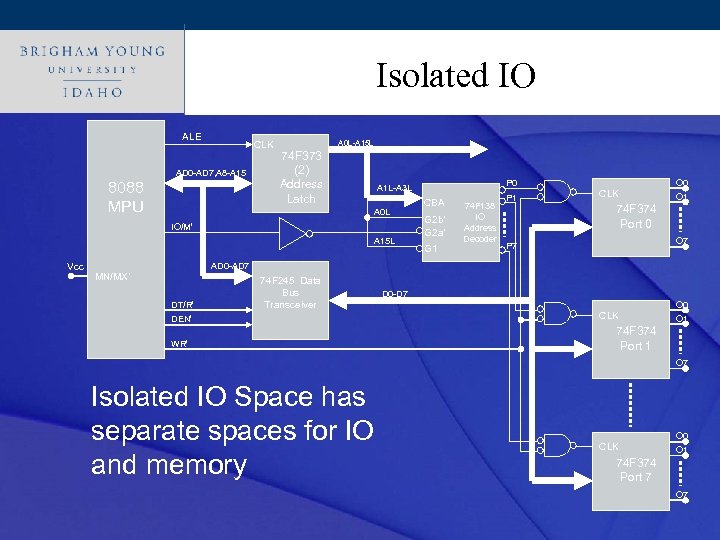
Click to edit Master title style Isolated IO ALE CLK AD 0 -AD 7, A 8 -A 15 8088 MPU A 0 L-A 15 L 74 F 373 (2) Address Latch A 0 L IO/M’ A 15 L Vcc P 0 A 1 L-A 3 L CBA G 2 b’ G 2 a’ G 1 74 F 138 IO Address Decoder P 1 CLK O 0 O 1 74 F 374 Port 0 O 7 P 7 AD 0 -AD 7 MN/MX’ DT/R’ 74 F 245 Data Bus Transceiver DEN’ WR’ D 0 -D 7 CLK O 0 O 1 74 F 374 Port 1 O 7 Isolated IO Space has separate spaces for IO and memory CLK O 0 O 1 74 F 374 Port 7 O 7
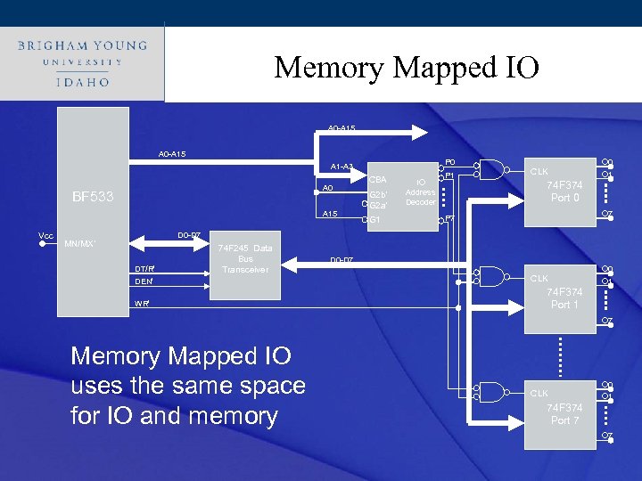
Click to edit Master title style Memory Mapped IO A 0 -A 15 P 0 A 1 -A 3 A 0 BF 533 A 15 Vcc CBA G 2 b’ G 2 a’ G 1 IO Address Decoder P 1 CLK O 0 O 1 74 F 374 Port 0 O 7 P 7 D 0 -D 7 MN/MX’ DT/R’ DEN’ 74 F 245 Data Bus Transceiver WR’ D 0 -D 7 CLK O 0 O 1 74 F 374 Port 1 O 7 Memory Mapped IO uses the same space for IO and memory CLK O 0 O 1 74 F 374 Port 7 O 7
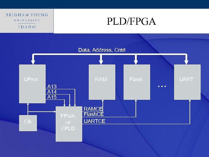
Click to edit Master title style PLD/FPGA Data, Address, Cntrl UProc RAM A 13 A 14 A 15 Clk FPGA or CPLD RAMCE Flash. CE UARTCE Flash … UART
Click. Signal Overloading style to edit Master title • What is signal overloading? • Caused by connecting too many input circuits to a single output • Also called Fan-out or loading problem • How can you tell if you have a loading problem? • • Data Sheets specify the current a device is able to drive on its output lines Data Sheets also specify the current a device will typically source on its input lines • How can you solve this? • Figure 2. 19 in text
There is no such thing as Digital!!! Click to edit Master title style • All signals are really analog • It takes a finite amount of time for a signal to travel from one point to another. High speed digital designers need to understand this • Timing diagrams show actual AC timings including propagation delay. http: //emp. byui. edu/FISHERR/All_Classes/Digital/74 ls 00. pdf
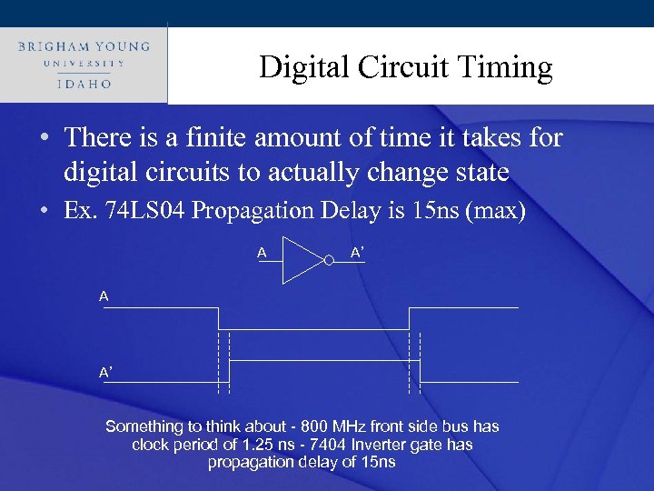
Click to edit Master title style Digital Circuit Timing • There is a finite amount of time it takes for digital circuits to actually change state • Ex. 74 LS 04 Propagation Delay is 15 ns (max) A A’ Something to think about - 800 MHz front side bus has clock period of 1. 25 ns - 7404 Inverter gate has propagation delay of 15 ns
Click to edit Master title style Digital Circuit Timing • There are several key timing characteristics associated with digital circuits • • • Propagation Delay Setup Time Hold Time Max Clock Frequency Clock pulse high and low times
Click Propagation Delay style to edit Master title • Propagation Delay is the time it takes for the output of the circuit to change after the input has changed. • Depending on technologies (TTL, CMOS, ECL, etc), propagation delay’s of modern IC’s range from <1 ns to ~100 ns.
Click to edit Master title style Setup Time • The setup time is the time interval immediately preceding the active transition of the CLK signal during which the control input must be maintained at the proper level. • If this time is not met, the FF may not respond to the CLK appropriately
Click to edit Master title style Hold Time • Hold Time is the time interval immediately following the active transition of the CLK signal during which the synchronous control input must be maintained at the proper level. • If this time is not met, the FF may not respond to the CLK appropriately
Click to edit Master title style Clock Frequency Spec’s • Max Frequency (Fmax) - This is the highest frequency that may be applied to the CLK input and still have it trigger reliability • Clock Pulse High (Twh) and Clock Pulse Low (Twl) Times – These are the minimum time duration that the clock signal must remain low before it goes high (Twl) and high before it returns low (Twh)
Click to edit Master title style Timings • How can we ensure each device can talk to the microprocessor? • 3 Methods • • • Wait states – figure 3. 6 and 3. 7 Wait signal – figure 3. 5 Buy fast enough parts - $$$
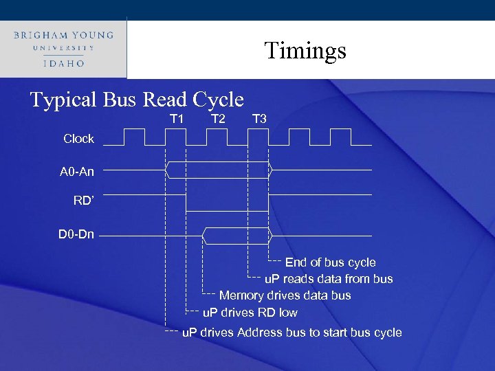
Click to edit Master title style Timings Typical Bus Read Cycle T 1 T 2 T 3 Clock A 0 -An RD’ D 0 -Dn End of bus cycle u. P reads data from bus Memory drives data bus u. P drives RD low u. P drives Address bus to start bus cycle
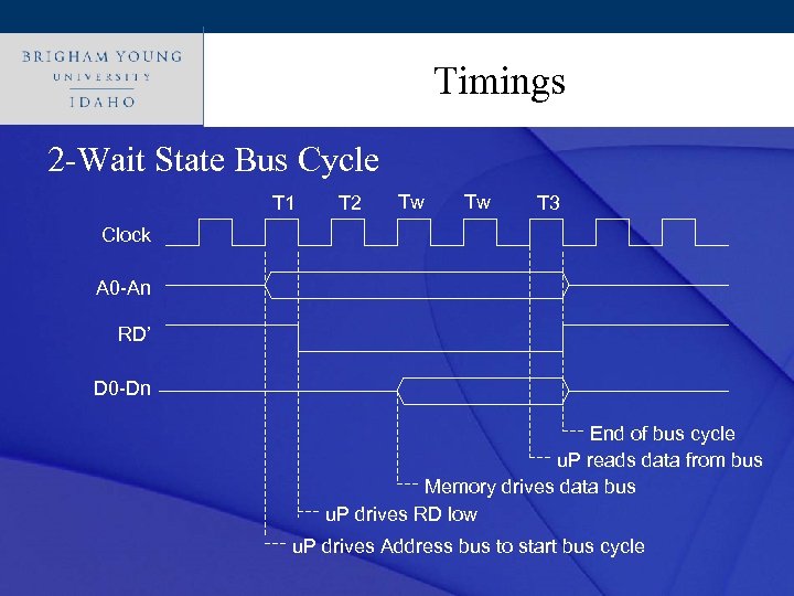
Click to edit Master title style Timings 2 -Wait State Bus Cycle T 1 T 2 Tw Tw T 3 Clock A 0 -An RD’ D 0 -Dn End of bus cycle u. P reads data from bus Memory drives data bus u. P drives RD low u. P drives Address bus to start bus cycle
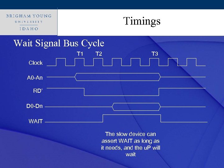
Timings Click to edit Master title style Wait Signal Bus Cycle T 1 T 2 T 3 Clock A 0 -An RD’ D 0 -Dn WAIT The slow device can assert WAIT as long as it needs, and the u. P will wait

Backup
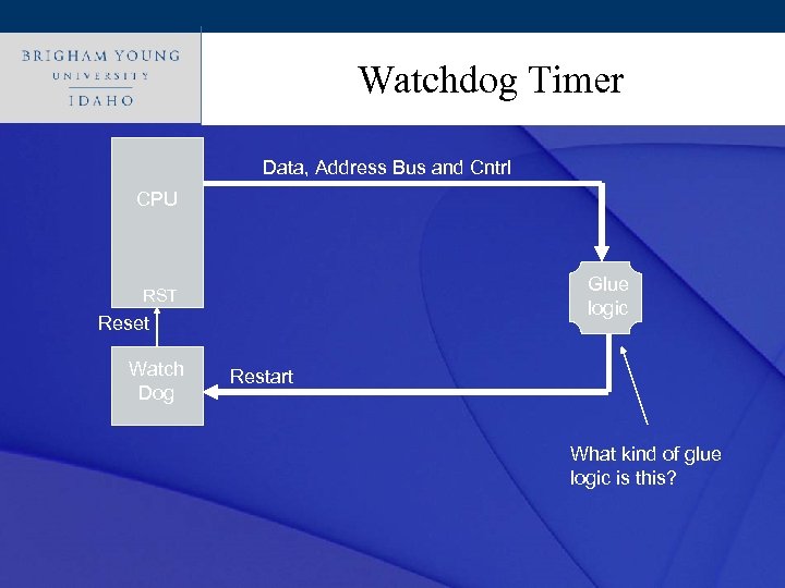
Click to edit Master title style Watchdog Timer Data, Address Bus and Cntrl CPU Glue logic RST Reset Watch Dog Restart What kind of glue logic is this?
Click to edit Master title style DMA’s • Direct Memory Access (DMA) • • Circuitry that can read/write data to/from an IO device and memory Independent from processor • Need to have arbitration between DMA and processor
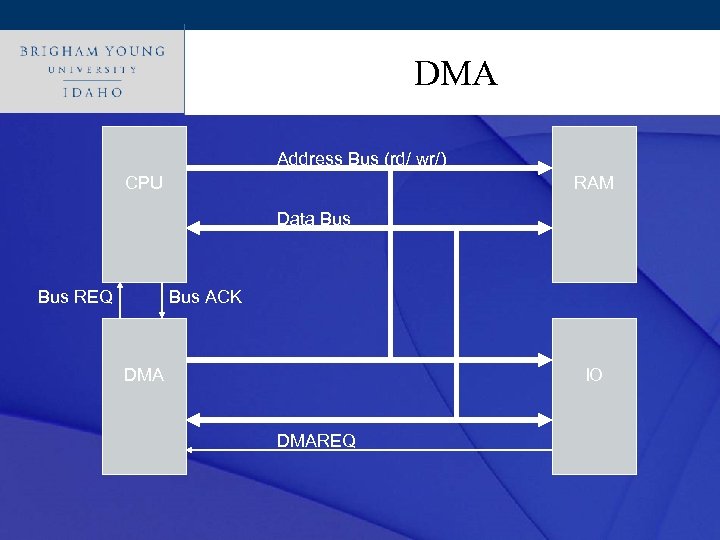
Click to edit. DMA title style Master Address Bus (rd/ wr/) CPU RAM Data Bus REQ Bus ACK DMA IO DMAREQ
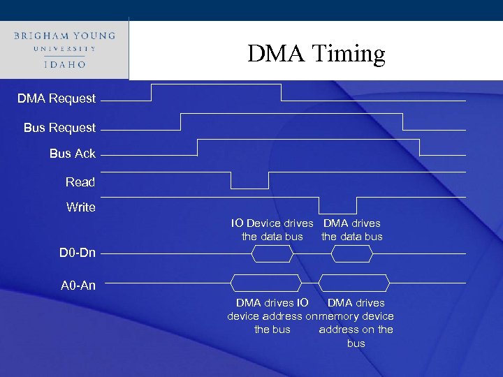
Click to. DMA Timing style edit Master title DMA Request Bus Ack Read Write IO Device drives DMA drives the data bus D 0 -Dn A 0 -An DMA drives IO DMA drives device address on memory device the bus address on the bus
c150beb62d6520f86bc0311380c3b394.ppt