b593d7aaa7b3a9c6529fc924add14bfb.ppt
- Количество слайдов: 20
 COE 4 OI 5 Engineering Design Chapter 2: UP 2/UP 3 board
 UP 3 • UP 3 board contains a Cyclone FPGA, several memory devices and a wide range of I/O features • Two versions of the board are available one based on C 6 and the other one based on C 12 FPGA. • The FPGA and memory devices can be programmed using a JTAG Byte. Blaster II cable attached to the PC printer (parallel) port • The printer port mode of the PC should be set in the PC’s BIOS to ECP or EPP. Copyright S. Shirani 2
 UP 3 • An on-board clock oscillator and clock chip provides several clock signals that are selectable with the board’s jumpers Copyright S. Shirani 3
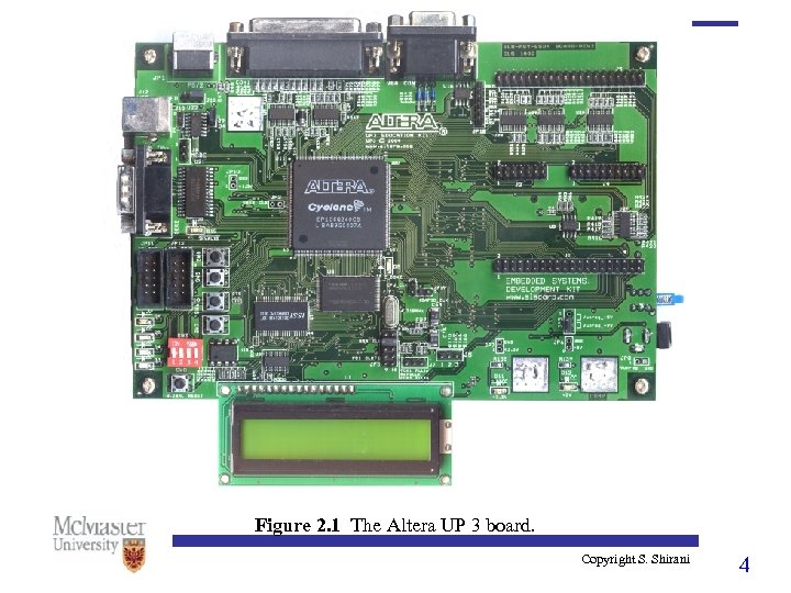 Figure 2. 1 The Altera UP 3 board. Copyright S. Shirani 4
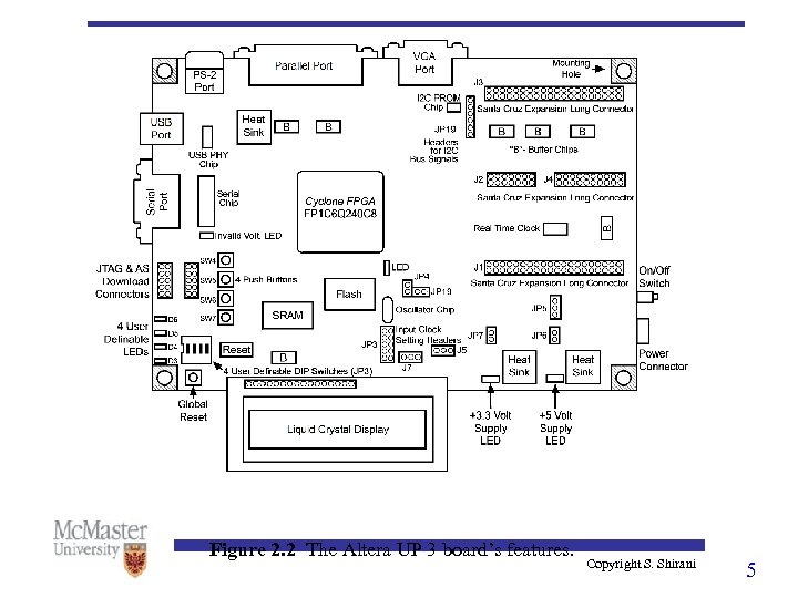 Figure 2. 2 The Altera UP 3 board’s features. Copyright S. Shirani 5
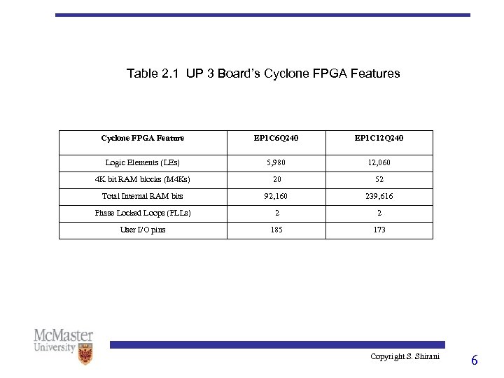 Table 2. 1 UP 3 Board’s Cyclone FPGA Feature EP 1 C 6 Q 240 EP 1 C 12 Q 240 Logic Elements (LEs) 5, 980 12, 060 4 K bit RAM blocks (M 4 Ks) 20 52 Total Internal RAM bits 92, 160 239, 616 Phase Locked Loops (PLLs) 2 2 User I/O pins 185 173 Copyright S. Shirani 6
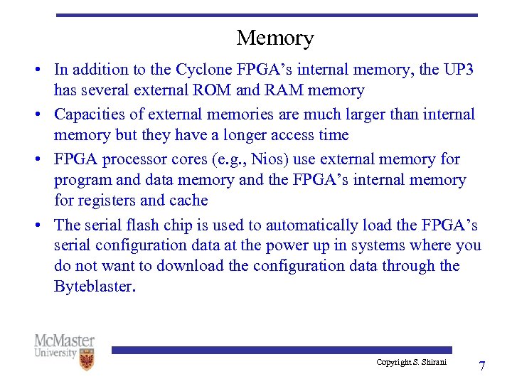 Memory • In addition to the Cyclone FPGA’s internal memory, the UP 3 has several external ROM and RAM memory • Capacities of external memories are much larger than internal memory but they have a longer access time • FPGA processor cores (e. g. , Nios) use external memory for program and data memory and the FPGA’s internal memory for registers and cache • The serial flash chip is used to automatically load the FPGA’s serial configuration data at the power up in systems where you do not want to download the configuration data through the Byteblaster. Copyright S. Shirani 7
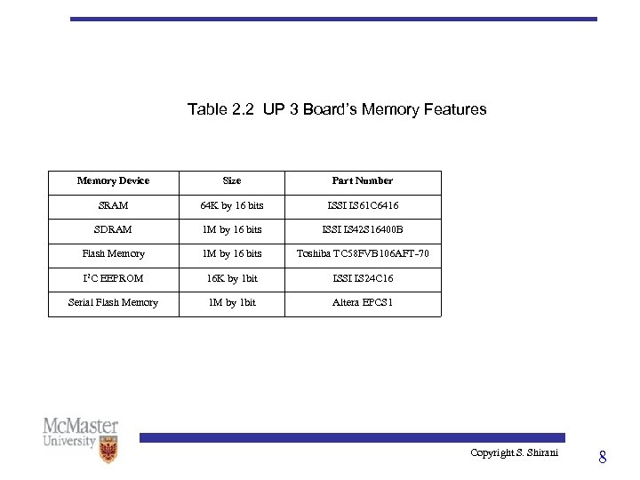 Table 2. 2 UP 3 Board’s Memory Features Memory Device Size Part Number SRAM 64 K by 16 bits ISSI IS 61 C 6416 SDRAM 1 M by 16 bits ISSI IS 42 S 16400 B Flash Memory 1 M by 16 bits Toshiba TC 58 FVB 106 AFT-70 I 2 C EEPROM 16 K by 1 bit ISSI IS 24 C 16 Serial Flash Memory 1 M by 1 bit Altera EPCS 1 Copyright S. Shirani 8
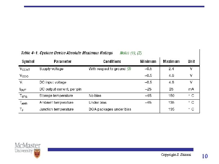
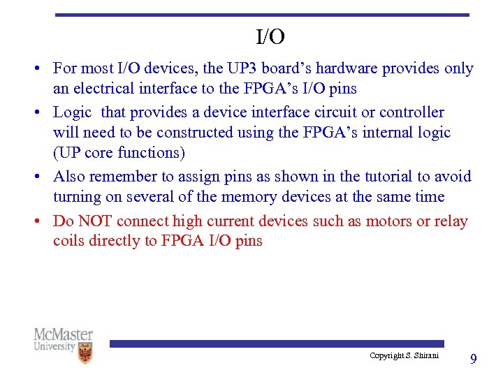 I/O • For most I/O devices, the UP 3 board’s hardware provides only an electrical interface to the FPGA’s I/O pins • Logic that provides a device interface circuit or controller will need to be constructed using the FPGA’s internal logic (UP core functions) • Also remember to assign pins as shown in the tutorial to avoid turning on several of the memory devices at the same time • Do NOT connect high current devices such as motors or relay coils directly to FPGA I/O pins Copyright S. Shirani 9
 Copyright S. Shirani 10
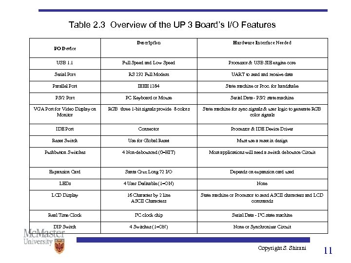 Table 2. 3 Overview of the UP 3 Board’s I/O Features Description Hardware Interface Needed USB 1. 1 Full Speed and Low Speed Processor & USB SIE engine core Serial Port RS 232 Full Modem UART to send and receive data Parallel Port IEEE 1284 State machine or Proc. for handshake PS/2 Port PC Keyboard or Mouse Serial Data - PS/2 state machine VGA Port for Video Display on Monitor RGB three 1 -bit signals provide 8 colors State machine for sync signals & user logic to generate RGB color signals IDE Port Connector Processor & IDE Device Driver Reset Switch Use for Global Reset Must use a reset in design Pushbutton Switches 4 Non-debounced (0=HIT) Most applications will need a switch debounce Circuit Expansion Card Santa Cruz Long 72 I/O Depends on expansion card used LEDs 4 User Definable (1=ON) None LCD Display 16 Character by 2 line ASCII Characters State machine or Processor to send ASCII characters and LCD commands Real Time Clock I 2 C clock chip Serial Data - I 2 C state machine DIP Switch 4 Switches (1=ON) None or Synchronizer Circuit I/O Device Copyright S. Shirani 11
 Table 2. 4 UP 3 Board’s most commonly used FPGA I/O pin names and assignments Pin Name Pin# Pin I/O Type Function of Pin PS 2_CLK 12 Bidirectional PS 2 Connector PS 2_DATA 13 Bidirectional PS 2 Connector RESET 23 Input Power on or SW 8 pushbutton reset ( Reset = 0 ) USB_CLK 29 Input USB 48 MHz Clock - jumper USER_CLOCK 38 Input External Clock from J 2 Pin 2 PBSWITCH_4 48 Input Pushbutton SW 4 (non-debounced, 0 = button hit) PBSWITCH_5 49 Input Pushbutton SW 5 (non-debounced, 0 = button hit) LCD_E 50 Output LCD Enable line LED_D 6 53 Output LED D 3 (0 = LED ON, 1= LED OFF) LED_D 5 54 Output LED D 4 (0 = LED ON, 1= LED OFF) LED_D 4 55 Output LED D 5 (0 = LED ON, 1= LED OFF) LED_D 3 56 Output LED D 6 (0 = LED ON, 1= LED OFF) PBSWITCH_6 57 Input Pushbutton SW 6 (non-debounced, 0 = hit) DIPSWITCH_1 58 Input DIP Switch SW 3 #1 ( ON = 1, OFF = 0) DIPSWITCH_2 59 Input DIP Switch SW 3 #2 ( ON = 1, OFF = 0) DIPSWITCH_3 60 Input DIP Switch SW 3 #3 ( ON = 1, OFF = 0)" DIPSWITCH_4 61 Input DIP Switch SW 3 #4 ( ON = 1, OFF = 0) Copyright S. Shirani 12
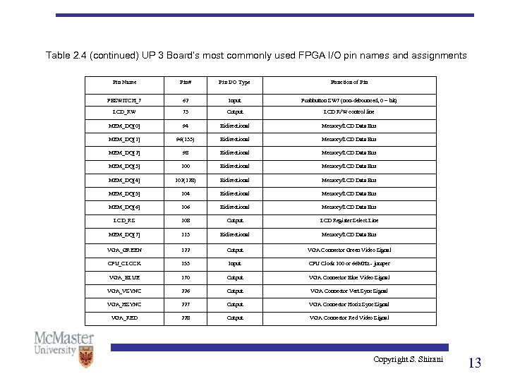 Table 2. 4 (continued) UP 3 Board’s most commonly used FPGA I/O pin names and assignments Pin Name Pin# Pin I/O Type Function of Pin PBSWITCH_7 62 Input Pushbutton SW 7 (non-debounced, 0 = hit) LCD_RW 73 Output LCD R/W control line MEM_DQ[0] 94 Bidirectional Memory/LCD Data Bus MEM_DQ[1] 96(133) Bidirectional Memory/LCD Data Bus MEM_DQ[2] 98 Bidirectional Memory/LCD Data Bus MEM_DQ[3] 100 Bidirectional Memory/LCD Data Bus MEM_DQ[4] 102(128) Bidirectional Memory/LCD Data Bus MEM_DQ[5] 104 Bidirectional Memory/LCD Data Bus MEM_DQ[6] 106 Bidirectional Memory/LCD Data Bus LCD_RS 108 Output LCD Register Select Line MEM_DQ[7] 113 Bidirectional Memory/LCD Data Bus VGA_GREEN 122 Output VGA Connector Green Video Signal CPU_CLOCK 153 Input CPU Clock 100 or 66 MHz - jumper VGA_BLUE 170 Output VGA Connector Blue Video Signal VGA_VSYNC 226 Output VGA Connector Vert Sync Signal VGA_HSYNC 227 Output VGA Connector Horiz Sync Signal VGA_RED 228 Output VGA Connector Red Video Signal Copyright S. Shirani 13
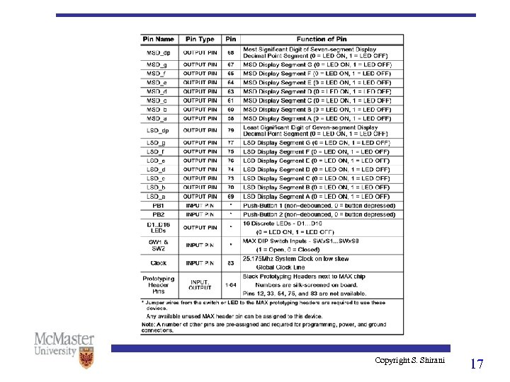
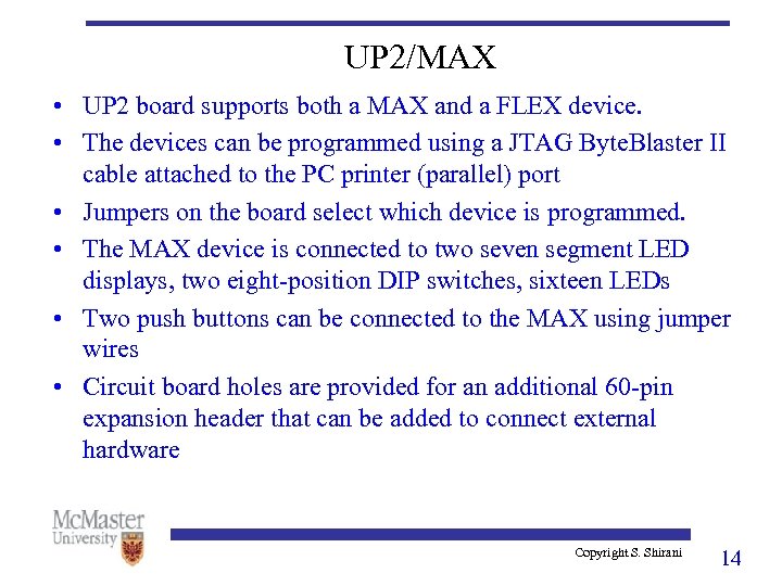 UP 2/MAX • UP 2 board supports both a MAX and a FLEX device. • The devices can be programmed using a JTAG Byte. Blaster II cable attached to the PC printer (parallel) port • Jumpers on the board select which device is programmed. • The MAX device is connected to two seven segment LED displays, two eight-position DIP switches, sixteen LEDs • Two push buttons can be connected to the MAX using jumper wires • Circuit board holes are provided for an additional 60 -pin expansion header that can be added to connect external hardware Copyright S. Shirani 14
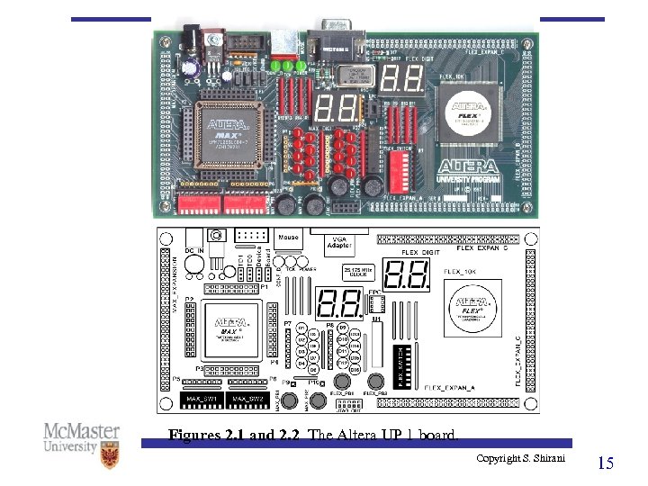 Figures 2. 1 and 2. 2 The Altera UP 1 board. Copyright S. Shirani 15
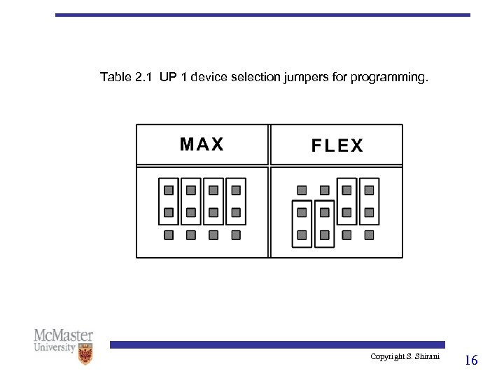 Table 2. 1 UP 1 device selection jumpers for programming. Copyright S. Shirani 16
 Copyright S. Shirani 17
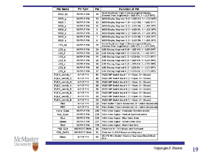
 UP 2/FLEX • FLEX device is attached to a VGA connector, a PS/2 mouse and keyboard port, two seven segment displays, an eightposition DIP switch and two push buttons. • To generate video output, mouse or keyboard input, an interface must be designed using logic inside the FLEX device (UP core functions) • Circuit board holes are provided for three 60 -pin expansion header that can be added to connect external hardware • Do NOT connect high current devices such as motors or relay coils directly to FPGA I/O pins Copyright S. Shirani 18
 Copyright S. Shirani 19
 Copyright S. Shirani 20


