9af9765d8983d4868ddd145f04d2bd94.ppt
- Количество слайдов: 27
 CMOS Image Sensors for non-HEP Applications Dr Renato Turchetta CMOS Sensor Design Group CCLRC Technology
 2 FEE 2006, 17 -20 May 2006, Perugia, Italy Outline Ø Introduction Ø CMOS for scientific applications Visible light UV X-ray Charged particles Voltage Ø Advanced pixels Ø Conclusions
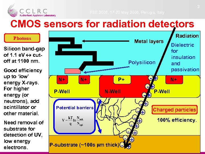 3 FEE 2006, 17 -20 May 2006, Perugia, Italy CMOS sensors for radiation detectors Photons Metal layers Silicon band-gap of 1. 1 e. V cutoff at 1100 nm. Good efficiency up to ‘low’ energy X-rays. For higher energy (or neutrons), add scintillator or other material. Need removal of substrate for detection of UV, low energy electrons. Polysilicon Radiation Dielectric for insulation and passivation -+ N+ -+ P-Well N-Well P-Well -+ -+ P-epitaxial Potential barriers - + Charged particles layer -+ (up to to 20 100% efficiency. -+ mm thick) - + P-substrate (~100 s mm thick) - + N+ N+ P+
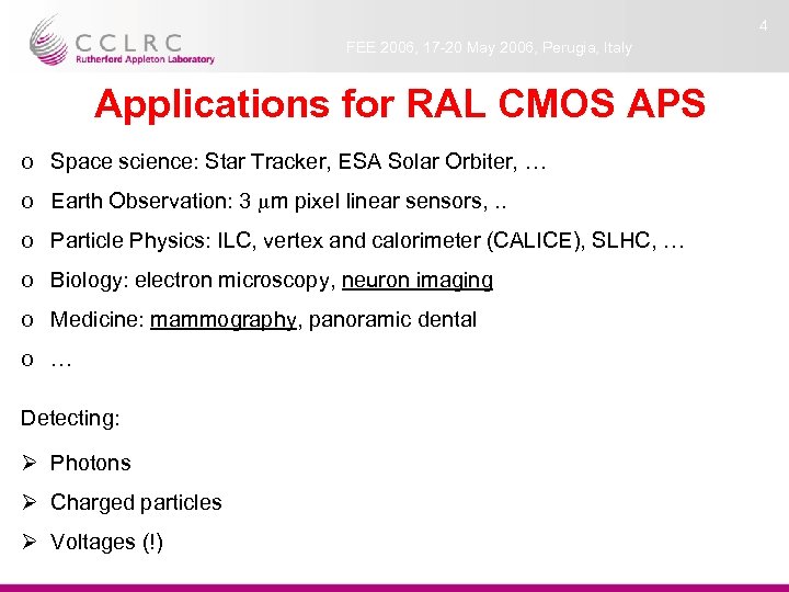 4 FEE 2006, 17 -20 May 2006, Perugia, Italy Applications for RAL CMOS APS o Space science: Star Tracker, ESA Solar Orbiter, … o Earth Observation: 3 mm pixel linear sensors, . . o Particle Physics: ILC, vertex and calorimeter (CALICE), SLHC, … o Biology: electron microscopy, neuron imaging o Medicine: mammography, panoramic dental o … Detecting: Ø Photons Ø Charged particles Ø Voltages (!)
 5 FEE 2006, 17 -20 May 2006, Perugia, Italy CMOS sensors requirements. 1 Ø Wide dynamic range: 16 bits and beyond Ø Low noise: <~ 10 e- rms < 1 e- rms ? Ø 4 T transistor with pinned diode Ø Radiation hardness: Mrad and beyond Ø Speed: data rate in excess of 50 MB/sec 500 MB/sec and beyond Short integration time and gating ns Ø Large pixels: >10 mm 50 mm Ø No data compression or lossless compression Ø Large volume of data: 100 s MB/sec for minutes, hours, …
 6 FEE 2006, 17 -20 May 2006, Perugia, Italy CMOS sensors requirements. 2 Ø Images can be mainly dark with only a few bright spots Ø Advanced pixel designs Ø In-pixel data reduction Ø Only NMOS in pixel if 100% efficiency for charged particle detection is required Ø Large area: side ~ cm’s; no focusing possible for X-ray or charged particles Ø SOI on high resistivity handle wafers full CMOS Ø Semiconductor deposition
 7 FEE 2006, 17 -20 May 2006, Perugia, Italy Outline Ø Introduction Ø CMOS for scientific applications Visible light UV X-ray Charged particles Voltage Ø Advanced pixels Ø Conclusions
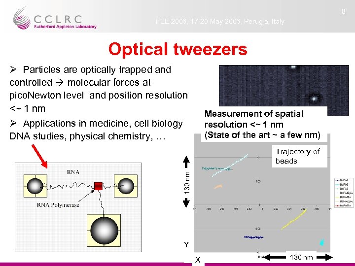 8 FEE 2006, 17 -20 May 2006, Perugia, Italy Optical tweezers Ø Particles are optically trapped and controlled molecular forces at pico. Newton level and position resolution <~ 1 nm Ø Applications in medicine, cell biology, DNA studies, physical chemistry, … Measurement of spatial resolution <~ 1 nm (State of the art ~ a few nm) 130 nm Trajectory of beads Y X 130 nm
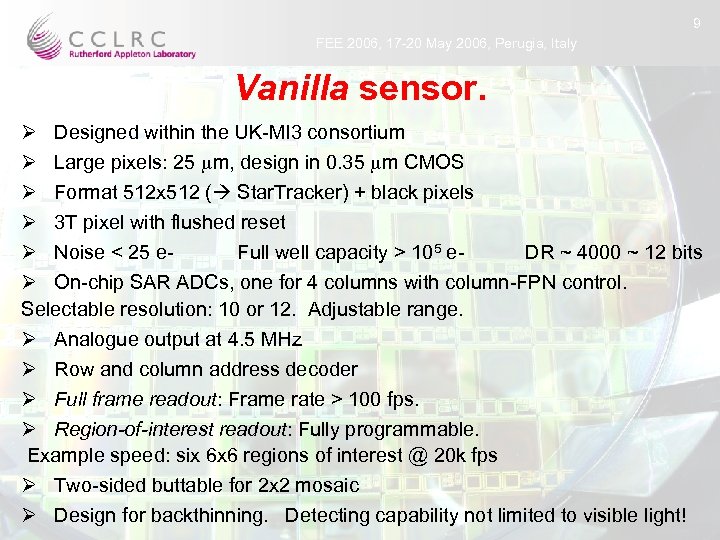 9 FEE 2006, 17 -20 May 2006, Perugia, Italy Vanilla sensor. Ø Designed within the UK-MI 3 consortium Ø Large pixels: 25 mm, design in 0. 35 mm CMOS Ø Format 512 x 512 ( Star. Tracker) + black pixels Ø 3 T pixel with flushed reset Ø Noise < 25 e. Full well capacity > 105 e. DR ~ 4000 ~ 12 bits Ø On-chip SAR ADCs, one for 4 columns with column-FPN control. Selectable resolution: 10 or 12. Adjustable range. Ø Analogue output at 4. 5 MHz Ø Row and column address decoder Ø Full frame readout: Frame rate > 100 fps. Ø Region-of-interest readout: Fully programmable. Example speed: six 6 x 6 regions of interest @ 20 k fps Ø Two-sided buttable for 2 x 2 mosaic Ø Design for backthinning. Detecting capability not limited to visible light!
 10 FEE 2006, 17 -20 May 2006, Perugia, Italy Outline Ø Introduction Ø CMOS for scientific applications Visible light UV X-ray Charged particles Voltage Ø Advanced pixels Ø Conclusions
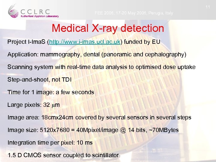 11 FEE 2006, 17 -20 May 2006, Perugia, Italy Medical X-ray detection Project I-Ima. S (http: //www. i-imas. ucl. ac. uk) funded by EU Application: mammography, dental (panoramic and cephalography) Scanning system with real-time data analysis to optimised dose uptake Step-and-shoot, not TDI Time for 1 image: a few seconds Large pixels: 32 mm Image area: 18 cmx 24 cm covered by several sensors in several steps Image size: 5120 x 7680 = 40 Mpixel/image @ 14 bits, ~70 MBytes Integration time per pixel: 10 ms 1. 5 D CMOS sensor coupled to scintillator
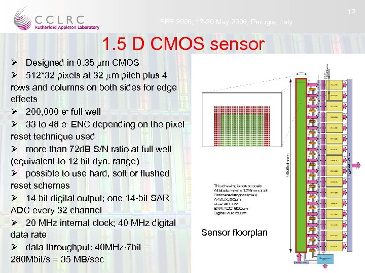 12 FEE 2006, 17 -20 May 2006, Perugia, Italy 1. 5 D CMOS sensor Ø Designed in 0. 35 mm CMOS Ø 512*32 pixels at 32 mm pitch plus 4 rows and columns on both sides for edge effects Ø 200, 000 e- full well Ø 33 to 48 e- ENC depending on the pixel reset technique used Ø more than 72 d. B S/N ratio at full well (equivalent to 12 bit dyn. range) Ø possible to use hard, soft or flushed reset schemes Ø 14 bit digital output; one 14 -bit SAR ADC every 32 channel Ø 20 MHz internal clock; 40 MHz digital data rate Ø data throughput: 40 MHz· 7 bit = 280 Mbit/s = 35 MB/sec Sensor floorplan
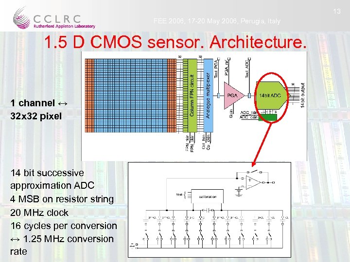 13 FEE 2006, 17 -20 May 2006, Perugia, Italy 1. 5 D CMOS sensor. Architecture. 1 channel ↔ 32 x 32 pixel 14 bit successive approximation ADC 4 MSB on resistor string 20 MHz clock 16 cycles per conversion ↔ 1. 25 MHz conversion rate
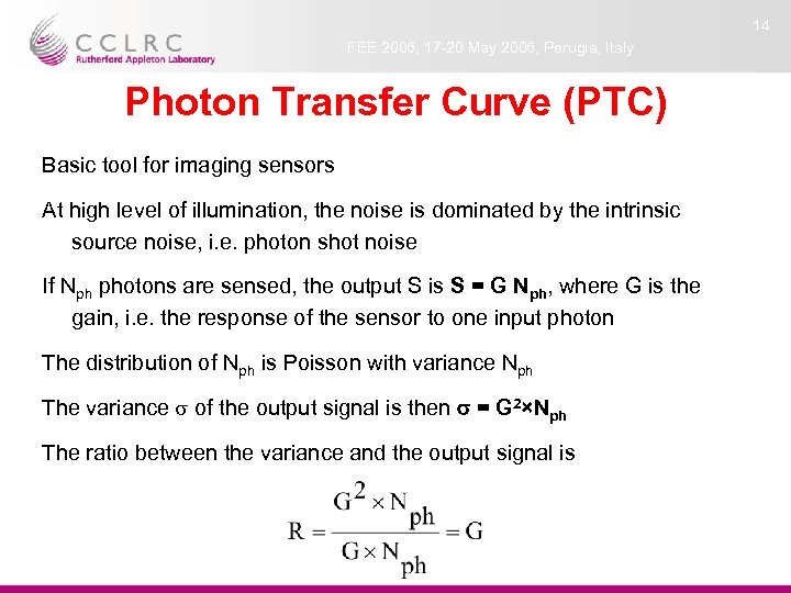 14 FEE 2006, 17 -20 May 2006, Perugia, Italy Photon Transfer Curve (PTC) Basic tool for imaging sensors At high level of illumination, the noise is dominated by the intrinsic source noise, i. e. photon shot noise If Nph photons are sensed, the output S is S = G Nph, where G is the gain, i. e. the response of the sensor to one input photon The distribution of Nph is Poisson with variance Nph The variance of the output signal is then s = G 2×Nph The ratio between the variance and the output signal is
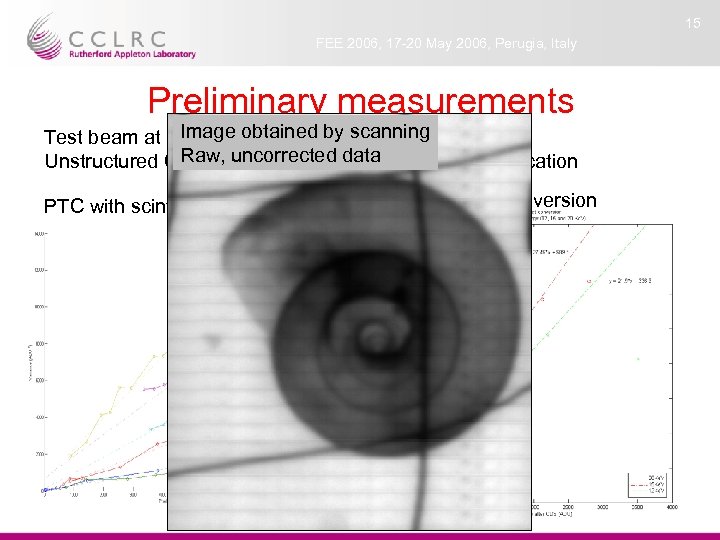 15 FEE 2006, 17 -20 May 2006, Perugia, Italy Preliminary measurements Image obtained by scanning Test beam at Elettra synchrotron, Trieste, Italy Raw, uncorrected data Unstructured Cs. I scintillator, non optimum for the application PTC with scintillator Direct X-ray conversion
 16 FEE 2006, 17 -20 May 2006, Perugia, Italy Outline Ø Introduction Ø CMOS for scientific applications Visible light UV X-ray Charged particles Voltage Ø Advanced pixels Ø Conclusions
 17 FEE 2006, 17 -20 May 2006, Perugia, Italy APS for Neuroscience (NAPS) Goal of the project: study the spiking rate of a large number of neurons in parallel, each neuron being located with good spatial resolution across the surface of the visual cortex and with some depth discrimination. Project involving the Universities of Birmingham, Oxford, Cambridge and Berkeley (US) and RAL.
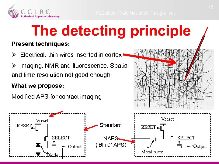 18 FEE 2006, 17 -20 May 2006, Perugia, Italy The detecting principle Present techniques: Ø Electrical: thin wires inserted in cortex Ø Imaging: NMR and fluorescence. Spatial and time resolution not good enough What we propose: Modified APS for contact imaging RESET Vreset Standard SELECT Output Diode RESET SELECT NAPS (‘Blind’ APS) Metal plate Output
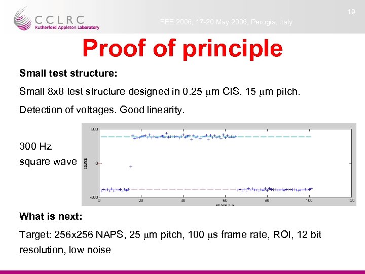 19 FEE 2006, 17 -20 May 2006, Perugia, Italy Proof of principle Small test structure: Small 8 x 8 test structure designed in 0. 25 mm CIS. 15 mm pitch. Detection of voltages. Good linearity. 300 Hz square wave What is next: Target: 256 x 256 NAPS, 25 mm pitch, 100 ms frame rate, ROI, 12 bit resolution, low noise
 20 FEE 2006, 17 -20 May 2006, Perugia, Italy Outline Ø Introduction. Ø CMOS for scientific applications Visible light UV X-ray Charged particles Voltage Ø Advanced pixels Ø Conclusions
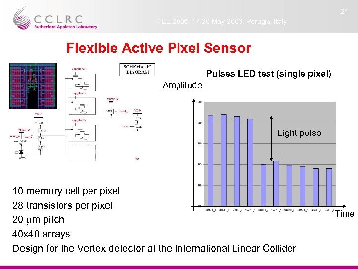 21 FEE 2006, 17 -20 May 2006, Perugia, Italy Flexible Active Pixel Sensor Pulses LED test (single pixel) Amplitude Light pulse 10 memory cell per pixel 28 transistors per pixel 20 mm pitch 40 x 40 arrays Design for the Vertex detector at the International Linear Collider Time
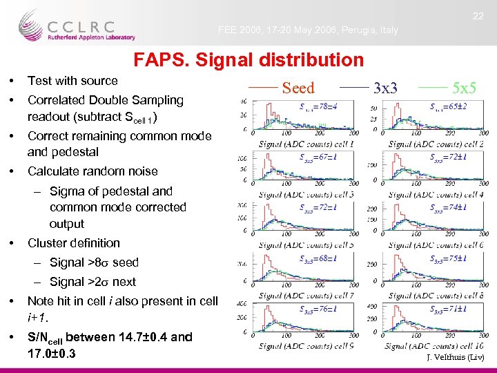 22 FEE 2006, 17 -20 May 2006, Perugia, Italy FAPS. Signal distribution • Test with source • Correlated Double Sampling readout (subtract Scell 1) • Correct remaining common mode and pedestal • Calculate random noise Seed 3 x 3 5 x 5 – Sigma of pedestal and common mode corrected output • Cluster definition – Signal >8 seed – Signal >2 next • Note hit in cell i also present in cell i+1. • S/Ncell between 14. 7± 0. 4 and 17. 0± 0. 3 J. Velthuis (Liv)
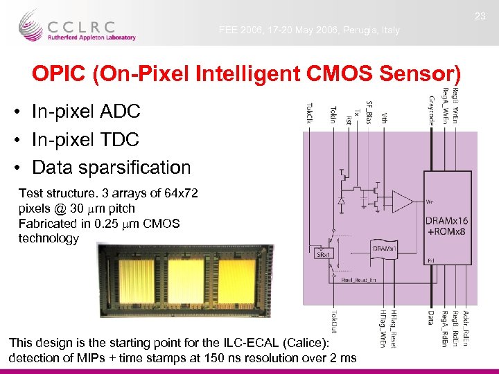 23 FEE 2006, 17 -20 May 2006, Perugia, Italy OPIC (On-Pixel Intelligent CMOS Sensor) • In-pixel ADC • In-pixel TDC • Data sparsification Test structure. 3 arrays of 64 x 72 pixels @ 30 mm pitch Fabricated in 0. 25 mm CMOS technology This design is the starting point for the ILC-ECAL (Calice): detection of MIPs + time stamps at 150 ns resolution over 2 ms
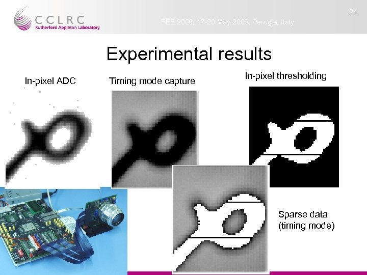 24 FEE 2006, 17 -20 May 2006, Perugia, Italy Experimental results In-pixel ADC Timing mode capture In-pixel thresholding Sparse data (timing mode)
 25 FEE 2006, 17 -20 May 2006, Perugia, Italy Outline Ø Introduction. Ø CMOS for scientific applications Visible light UV X-ray Charged particles Voltage Ø Advanced pixels Ø Conclusions
 26 FEE 2006, 17 -20 May 2006, Perugia, Italy Conclusions CMOS Image Sensors can be used to detect photons from IR down to low energy X-rays (direct detection), X-rays (indirect detection) and charged particles (direct detection with 100% efficiency) … and voltages Demonstrators built For some applications, large sensors already built Working towards delivery of CMOS Image Sensors-based for scientific instruments for space-science, particle physics and biomedical applications And last but not least …
 27 FEE 2006, 17 -20 May 2006, Perugia, Italy Acknowledgements N. Allinson (Sheffield U) + MI 3 collaboration G. Hall, Imperial College R. Speller (UCL) + I-Ima. S collaboration J. Jones, Imperial College A. Fant, CCLRC-RAL M. Noy, Imperial College J. Crooks, CCLRC-RAL M. Tyndel, CCLRC-RAL A. Clark, CCLRC-RAL P. Allport, Liverpool University P. Gąsiorek, CCLRC-RAL P. Dauncey, Imperial College N. Guerrini, CCLRC-RAL N. Watson, Birmingham University R. Halsall, CCLRC-RAL P. Willmore, Birmingham University M. Key-Charriere, CCLRC-RAL B. Willmore, Berkeley University S. Martin, CCLRC-RAL D. Tolhurst, , Cambridge University N. Waltham, CCLRC-RAL I. Thomson, Oxford University M. French, CCLRC-RAL M. Towrie, CCLRC-RAL M. Prydderch, CCLRC-RAL A. Ward, CCLRC-RAL G. Villani, CCLRC-RAL +. . . all the others I forgot to mention!


