9bfb1ca58853ea7141bd5ec1866f8ba3.ppt
- Количество слайдов: 161
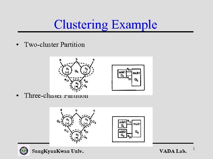 Clustering Example • Two-cluster Partition • Three-cluster Partition Sung. Kyun. Kwan Univ. VADA Lab. 1
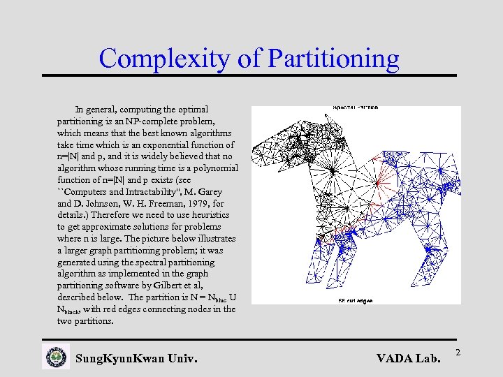 Complexity of Partitioning In general, computing the optimal partitioning is an NP-complete problem, which means that the best known algorithms take time which is an exponential function of n=|N| and p, and it is widely believed that no algorithm whose running time is a polynomial function of n=|N| and p exists (see ``Computers and Intractability'', M. Garey and D. Johnson, W. H. Freeman, 1979, for details. ) Therefore we need to use heuristics to get approximate solutions for problems where n is large. The picture below illustrates a larger graph partitioning problem; it was generated using the spectral partitioning algorithm as implemented in the graph partitioning software by Gilbert et al, described below. The partition is N = Nblue U Nblack, with red edges connecting nodes in the two partitions. Sung. Kyun. Kwan Univ. VADA Lab. 2
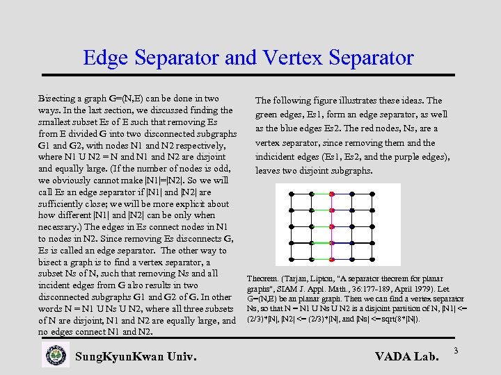 Edge Separator and Vertex Separator Bisecting a graph G=(N, E) can be done in two ways. In the last section, we discussed finding the smallest subset Es of E such that removing Es from E divided G into two disconnected subgraphs G 1 and G 2, with nodes N 1 and N 2 respectively, where N 1 U N 2 = N and N 1 and N 2 are disjoint and equally large. (If the number of nodes is odd, we obviously cannot make |N 1|=|N 2|. So we will call Es an edge separator if |N 1| and |N 2| are sufficiently close; we will be more explicit about how different |N 1| and |N 2| can be only when necessary. ) The edges in Es connect nodes in N 1 to nodes in N 2. Since removing Es disconnects G, Es is called an edge separator. The other way to bisect a graph is to find a vertex separator, a subset Ns of N, such that removing Ns and all incident edges from G also results in two disconnected subgraphs G 1 and G 2 of G. In other words N = N 1 U Ns U N 2, where all three subsets of N are disjoint, N 1 and N 2 are equally large, and no edges connect N 1 and N 2. Sung. Kyun. Kwan Univ. The following figure illustrates these ideas. The green edges, Es 1, form an edge separator, as well as the blue edges Es 2. The red nodes, Ns, are a vertex separator, since removing them and the indicident edges (Es 1, Es 2, and the purple edges), leaves two disjoint subgraphs. Theorem. (Tarjan, Lipton, "A separator theorem for planar graphs", SIAM J. Appl. Math. , 36: 177 -189, April 1979). Let G=(N, E) be an planar graph. Then we can find a vertex separator Ns, so that N = N 1 U Ns U N 2 is a disjoint partition of N, |N 1| <= (2/3)*|N|, |N 2| <= (2/3)*|N|, and |Ns| <= sqrt(8*|N|). VADA Lab. 3
 Kernighan and Lin Algorithm • • B. Kernighan and S. Lin ("An effective heuristic procedure for partitioning graphs", The Bell System Technial Journal, pp. 291 --308, Feb 1970), which takes O(|N|3) time per iteration. A more complicated and efficient implementation, which takes only O(|E|) time per iteration, was presented by C. Fiduccia and R. Mattheyses, "A linear-time heuristic for improving network partitions", Technical Report 82 CRD 130, General Electric Co. , Corporate Research and Development Ceter, Schenectady, NY 1982. We start with an edge weighted graph G=(N, E, WE), and a partitioning G = A U B into equal parts: |A| = |B|. Let w(e) = w(i, j) be the weight of edge e=(i, j), where the weight is 0 if no edge e=(i, j) exists. The goal is to find equal-sized subsets X in A and Y in B, such that exchanging X and Y reduces the total cost of edges from A to B. More precisely, we let T = sum[ a in A and b in B ] w(a, b) = cost of edges from A to B and seek X and Y such that new_A = A - X U Y and new_B = B - Y U X has a lower cost new_T. To compute new_T efficiently, we introduce: Sung. Kyun. Kwan Univ. E(a) = external cost of a = sum[ b in B ] w(a, b) I(a) = internal cost of a = sum[ a' in A, a'!=a]w(a, a') D(a) = cost of a = E(a) - I(a) and analogously E(b) = external cost of b = sum[ a in A ] w(a, b) I(b) = internal cost of b = sum[ b' in B, b' !=b]w(b, b') D(b) = cost of b = E(b) - I(b) Then it is easy to show that swapping a in A and b in B changes T to new_T = T - ( D(a) + D(b) 2*w(a, b) ) = T - gain(a, b) In other words, gain(a, b) = D(a)+D(b)-2*w(a, b) measures the improvement in the partitioning by swapping a and b. D(a') and D(b') also change to new_D(a') = D(a') + 2*w(a', a) - 2*w(a', b) for all a' in A, a' !=a new_D(b') = D(b') + 2*w(b', b) - 2*w(b', a) for all b' in B, b' != b VADA Lab. 4
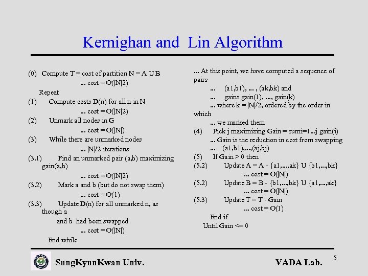 Kernighan and Lin Algorithm (0) Compute T = cost of partition N = A U B. . . cost = O(|N|2) Repeat (1) Compute costs D(n) for all n in N. . . cost = O(|N|2) (2) Unmark all nodes in G. . . cost = O(|N|) (3) While there are unmarked nodes. . . |N|/2 iterations (3. 1) Find an unmarked pair (a, b) maximizing gain(a, b). . . cost = O(|N|2) (3. 2) Mark a and b (but do not swap them). . . cost = O(1) (3. 3) Update D(n) for all unmarked n, as though a and b had been swapped. . . cost = O(|N|) End while Sung. Kyun. Kwan Univ. . At this point, we have computed a sequence of pairs. . . (a 1, b 1), . . . , (ak, bk) and. . . gains gain(1), . . . , gain(k). . . where k = |N|/2, ordered by the order in which. . . we marked them (4) Pick j maximizing Gain = sumi=1. . . j gain(i). . . Gain is the reduction in cost from swapping. . . (a 1, b 1), . . . , (aj, bj) (5) If Gain > 0 then (5. 2) Update A = A - {a 1, . . . , ak} U {b 1, . . . , bk}. . . cost = O(|N|) (5. 2) Update B = B - {b 1, . . . , bk} U {a 1, . . . , ak}. . . cost = O(|N|) (5. 3) Update T = T - Gain. . . cost = O(1) End if Until Gain <= 0 VADA Lab. 5
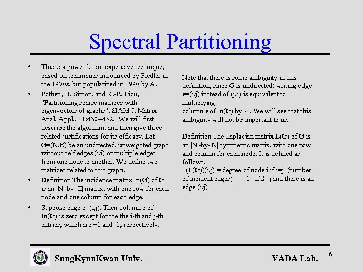 Spectral Partitioning • • This is a powerful but expensive technique, based on techniques introduced by Fiedler in the 1970 s, but popularized in 1990 by A. Pothen, H. Simon, and K. -P. Liou, "Partitioning sparse matrices with eigenvectors of graphs", SIAM J. Matrix Anal. Appl. , 11: 430 --452. We will first describe the algorithm, and then give three related justifications for its efficacy. Let G=(N, E) be an undirected, unweighted graph without self edges (i, i) or multiple edges from one node to another. We define two matrices related to this graph. Definition The incidence matrix In(G) of G is an |N|-by-|E| matrix, with one row for each node and one column for each edge. Suppose edge e=(i, j). Then column e of In(G) is zero except for the i-th and j-th entries, which are +1 and -1, respectively. Sung. Kyun. Kwan Univ. Note that there is some ambiguity in this definition, since G is undirected; writing edge e=(i, j) instead of (j, i) is equivalent to multiplying column e of In(G) by -1. We will see that this ambiguity will not be important to us. Definition The Laplacian matrix L(G) of G is an |N|-by-|N| symmetric matrix, with one row and column for each node. It is defined as follows. (L(G))(i, j) = degree of node i if i=j (number of incident edges) = -1 if i!=j and there is an edge (i, j) VADA Lab. 6
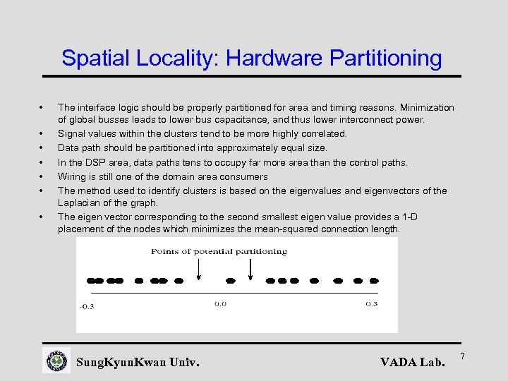 Spatial Locality: Hardware Partitioning • • The interface logic should be properly partitioned for area and timing reasons. Minimization of global busses leads to lower bus capacitance, and thus lower interconnect power. Signal values within the clusters tend to be more highly correlated. Data path should be partitioned into approximately equal size. In the DSP area, data paths tens to occupy far more area than the control paths. Wiring is still one of the domain area consumers The method used to identify clusters is based on the eigenvalues and eigenvectors of the Laplacian of the graph. The eigen vector corresponding to the second smallest eigen value provides a 1 -D placement of the nodes which minimizes the mean-squared connection length. Sung. Kyun. Kwan Univ. VADA Lab. 7
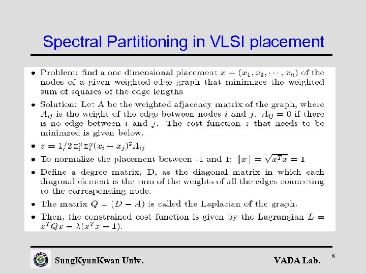 Spectral Partitioning in VLSI placement Sung. Kyun. Kwan Univ. VADA Lab. 8
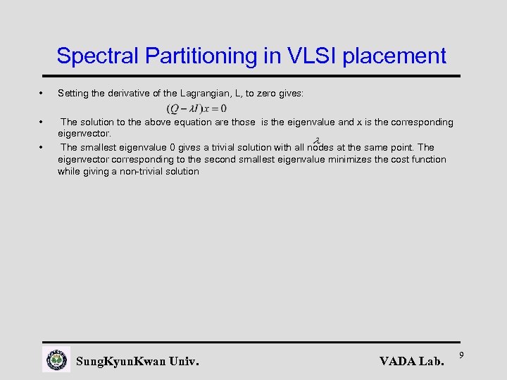 Spectral Partitioning in VLSI placement • Setting the derivative of the Lagrangian, L, to zero gives: • The solution to the above equation are those is the eigenvalue and x is the corresponding eigenvector. The smallest eigenvalue 0 gives a trivial solution with all nodes at the same point. The eigenvector corresponding to the second smallest eigenvalue minimizes the cost function while giving a non-trivial solution • Sung. Kyun. Kwan Univ. VADA Lab. 9
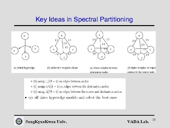 Key Ideas in Spectral Partitioning Sung. Kyun. Kwan Univ. VADA Lab. 10
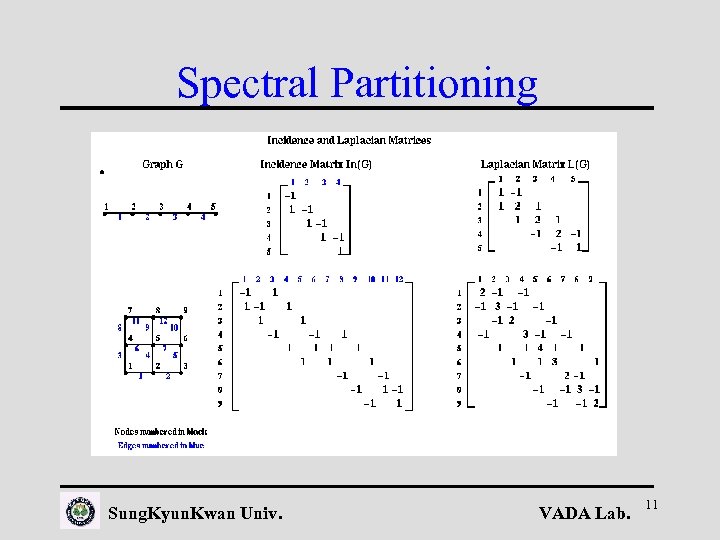 Spectral Partitioning Sung. Kyun. Kwan Univ. VADA Lab. 11
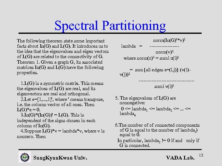 Spectral Partitioning The following theorem state some important facts about In(G) and L(G). It introduces us to the idea that the eigenvalues and eigen vectors of L(G) are related to the connectivity of G. Theorem 1. Given a graph G, its associated matrices In(G) and L(G) have the following properties. 1. L(G) is a symmetric matrix. This means the eigenvalues of L(G) are real, and its eigenvectors are real and orthogonal. 2. Let e=[1, . . . , 1]', where ' means transpose, i. e. the column vector of all ones. Then L(G)*e = 0. 3. In(G)*(In(G))' = L(G). This is independent of the signs chosen in each column of In(G). 4. Suppose L(G)*v = lambda*v, where v is nonzero. Then Sung. Kyun. Kwan Univ. norm(In(G)'*v)2 lambda = ---------norm(v)2 where norm(z)2 = sumi z(i)2 = sum{all edges e=(i, j)} (v(i)- v(j))2 -----------------sumi v(i)2 5. The eigenvalues of L(G) are nonnegative: 0 <= lambda 1 <= lambda 2 <=. . . <= lambdan 6. The number of of connected components of G is equal to the number of lambdai) equal to 0. In particular, lambda 2 != 0 if and only if G is connected. VADA Lab. 12
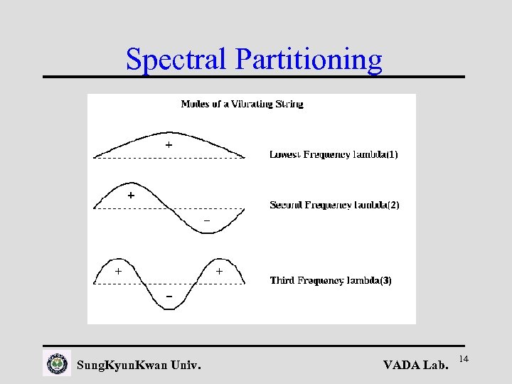
 Spectral Partitioning Compute the eigenvector v 2 corresponding to lambda 2 of L(G) for each node n of G if v 2(n) < 0 put node n in partition Nelse put node n in partition N+ endif endfor First we show that this partition is at least reasonable, because it tends to give connected components N- and N+: Theorem 2. (M. Fiedler, "A property of eigenvectors of nonnegative symmetric matrices and its application to graph theory", Czech. Math. J. 25: 619 --637, 1975. ) Let G be connected, and N- and N+ be defined by the above algorithm. Then N- is connected. If no v 2(n) = 0, N+ is also connected. Sung. Kyun. Kwan Univ. There a number of reasons lambda 2 is called the algebraic connectivity. Here is another. Theorem 3. (Fiedler). Let G=(N, E) be a graph, and G 1=(N, E 1) a subgraph, i. e. with the same nodes and subset of the edges, so that G 1 is "less connected" than G. Then lambda 2(L(G 1)) <= lambda 2(L(G)), i. e. the algebraic connectivity of G 1 is also less than or equal to the algebraic connectivity of G. Motivation for spectral bisection, by analogy with a vibrating string How does a taut string vibrate when it is plucked? From our background in either physics or music, we know that it has certain modes of vibration or harmonics. If we were to take snapshots of these modes, they would look like this: VADA Lab. 13
 Spectral Partitioning Sung. Kyun. Kwan Univ. VADA Lab. 14
 Multilevel Kernighan-Lin Given a matching, Gc is computed as follows. We let there be a node r in Nc for each edge in Gc is computed in step (1) of Recursive_partition as follows. We define a Em. Then we construct Ec as follows: matching of a graph G=(N, E) as a subset Em of the edges. E with the property that no for r = 1 to |Em|. . . for each node in Nc let (i, j) be the edge in Em corresponding to two edges in Em share an endpoint. A node r maximal matching is one to which no more for each other edge e=(i, k) in E incident on i edges can be added and remain a matching. let ek be the edge in Em incident on k, and We can compute a maximal matching by a let rk be the corresponding node in Nc simple random algorithm: add the edge (r, rk) to Ec end for let Em be empty for each other edge e=(j, k) in E incident on j mark all nodes in N as unmatched let ek be the edge in Em incident on k, and for i = 1 to |N|. . . visit the nodes in a let rk be the corresponding node in Nc random order add the edge (r, rk) to Ec if node i has not been matched, end for choose an edge e=(i, j) where j is also unmatched, end for and add it to Em if there are multiple edges between pairs of mark i and j as matched nodes of Nc, collapse them into single edges end if end for Sung. Kyun. Kwan Univ. VADA Lab. 15
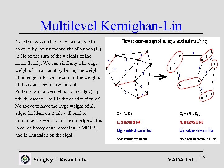 Multilevel Kernighan-Lin Note that we can take node weights into account by letting the weight of a node (i, j) in Nc be the sum of the weights of the nodes I and j. We can similarly take edge weights into account by letting the weight of an edge in Ec be the sum of the weights of the edges "collapsed" into it. Furthermore, we can choose the edge (i, j) which matches j to i in the construction of Nc above to have the large weight of all edges incident on i; this will tend to minimize the weights of the cut edges. This is called heavy edge matching in METIS, and is illustrated on the right. Sung. Kyun. Kwan Univ. VADA Lab. 16
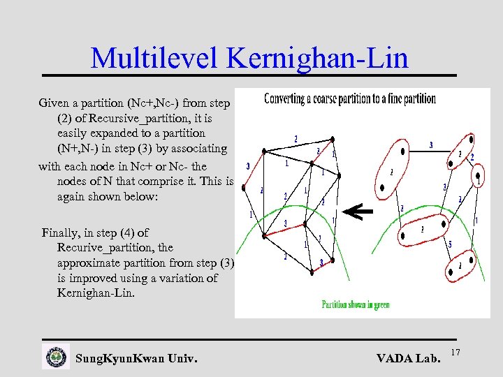 Multilevel Kernighan-Lin Given a partition (Nc+, Nc-) from step (2) of Recursive_partition, it is easily expanded to a partition (N+, N-) in step (3) by associating with each node in Nc+ or Nc- the nodes of N that comprise it. This is again shown below: Finally, in step (4) of Recurive_partition, the approximate partition from step (3) is improved using a variation of Kernighan-Lin. Sung. Kyun. Kwan Univ. VADA Lab. 17
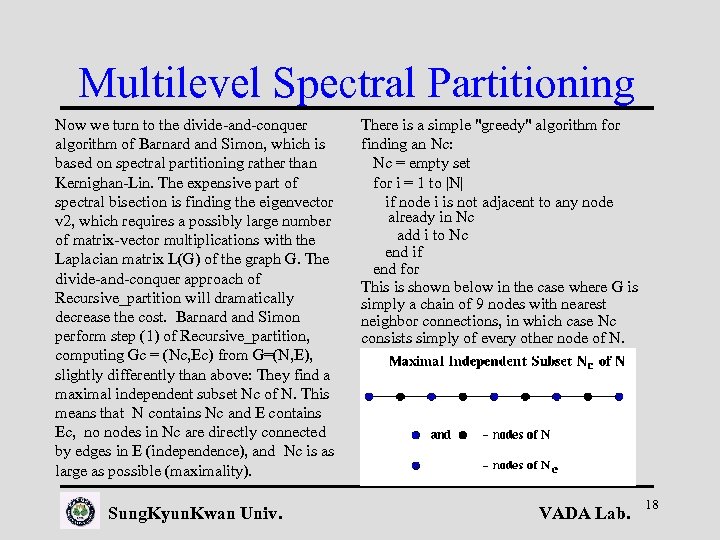 Multilevel Spectral Partitioning Now we turn to the divide-and-conquer algorithm of Barnard and Simon, which is based on spectral partitioning rather than Kernighan-Lin. The expensive part of spectral bisection is finding the eigenvector v 2, which requires a possibly large number of matrix-vector multiplications with the Laplacian matrix L(G) of the graph G. The divide-and-conquer approach of Recursive_partition will dramatically decrease the cost. Barnard and Simon perform step (1) of Recursive_partition, computing Gc = (Nc, Ec) from G=(N, E), slightly differently than above: They find a maximal independent subset Nc of N. This means that N contains Nc and E contains Ec, no nodes in Nc are directly connected by edges in E (independence), and Nc is as large as possible (maximality). Sung. Kyun. Kwan Univ. There is a simple "greedy" algorithm for finding an Nc: Nc = empty set for i = 1 to |N| if node i is not adjacent to any node already in Nc add i to Nc end if end for This is shown below in the case where G is simply a chain of 9 nodes with nearest neighbor connections, in which case Nc consists simply of every other node of N. VADA Lab. 18
 h. METIS • • • h. METIS is a set of programs for partitioning hypergraphs such as those corresponding to VLSI circuits. The algorithms implemented by h. METIS are based on the multilevel hypergraph partitioning scheme described in [KAKS 97]. h. METIS produces bisections that cut 10% to 300% fewer hyperedges than those cut by other popular algorithms such as PARABOLI, PROP, and CLIPPROP, especially for circuits with over 100, 000 cells, and circuits with nonunit cell area. It is extremely fast!A single run of h. METIS is faster than a single run of simpler schemes such as FM, KL, or CLIP. Furthermore, because of its very good average cut characteristics, it produces high quality partitionings in significantly fewer runs. It can bisect circuits with over 100, 000 vertices in a couple of minutes on Pentium-class workstations. The performance of h. METIS on the new ISPD 98 benchmark suite can be found in the paper by Chuck Alpert. = http: //www. users. cs. umn. edu/~karypis/metis. html Sung. Kyun. Kwan Univ. VADA Lab. 19
 How good is Recursive Bisection? • • Horst D. Simon and Shang-Hua Teng , Report RNR-93 -012, August 1993 The most commonly used p-way partitioning method is recursive bisection. It first "optimally" divides the graph (mesh) into two equal sized pieces and then recursively divides the two pieces. We show that, due to the greedy nature and the lack of global information, recursive bisection, in the worst case, may produce a partition that is very far from the optimal one. Our negative result is complemented by two positive ones. First, we show that for some important classes of graphs that occur in practical applications, such as well shaped finite element and finite difference meshes, recursive bisection is normally within a constant factor of the optimal one. Secondly, we show that if the balanced condition is relaxed so that each block in the partition is bounded by (1+e)n/p, then there exists a approximately balanced recursive partitioning scheme that finds a partition whose cost is within an 0(log p) factor of the cost of the optimal p-way partition. Sung. Kyun. Kwan Univ. VADA Lab. 20
 Partitioning Algorithm with Multiple Constraints 1998. 5. 19 조준동 Sung. Kyun. Kwan Univ. VADA Lab. 21
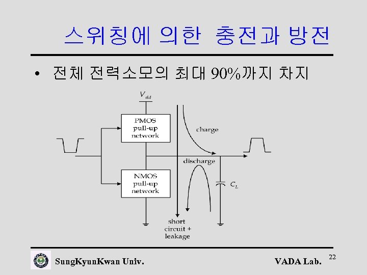 스위칭에 의한 충전과 방전 • 전체 전력소모의 최대 90%까지 차지 Sung. Kyun. Kwan Univ. VADA Lab. 22
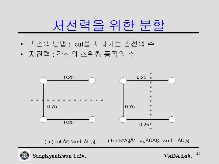 저전력을 위한 분할 • 기존의 방법 : cut을 지나가는 간선의 수 • 저전력 : 간선의 스위칭 동작의 수 Sung. Kyun. Kwan Univ. VADA Lab. 23
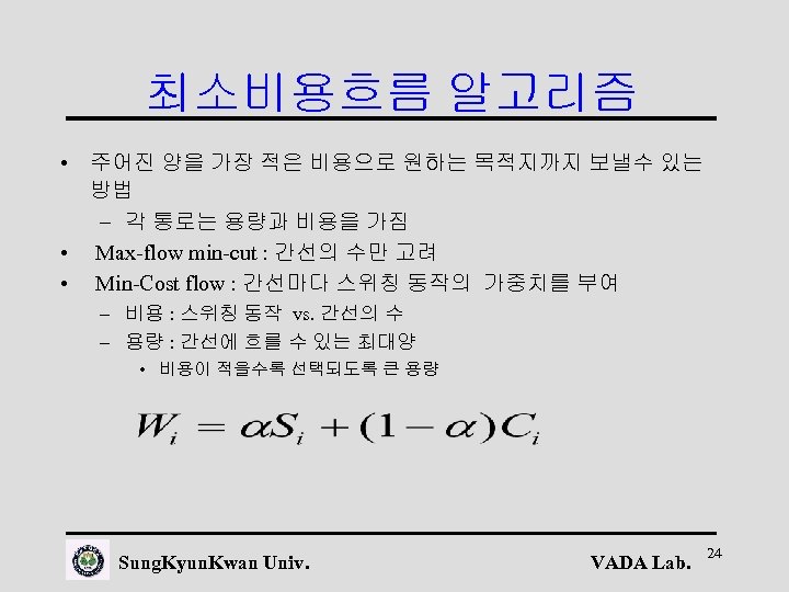 최소비용흐름 알고리즘 • 주어진 양을 가장 적은 비용으로 원하는 목적지까지 보낼수 있는 방법 – 각 통로는 용량과 비용을 가짐 • Max-flow min-cut : 간선의 수만 고려 • Min-Cost flow : 간선마다 스위칭 동작의 가중치를 부여 – 비용 : 스위칭 동작 vs. 간선의 수 – 용량 : 간선에 흐를 수 있는 최대양 • 비용이 적을수록 선택되도록 큰 용량 Sung. Kyun. Kwan Univ. VADA Lab. 24
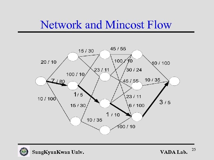 Network and Mincost Flow Sung. Kyun. Kwan Univ. VADA Lab. 25
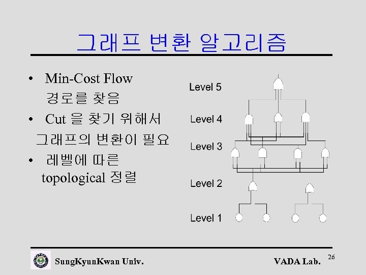 그래프 변환 알고리즘 • Min-Cost Flow 경로를 찾음 • Cut 을 찾기 위해서 그래프의 변환이 필요 • 레벨에 따른 topological 정렬 Sung. Kyun. Kwan Univ. VADA Lab. 26
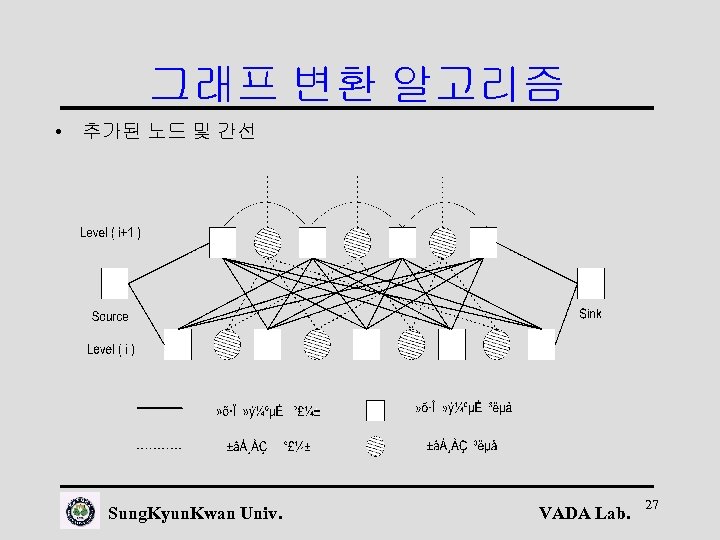 그래프 변환 알고리즘 • 추가된 노드 및 간선 Sung. Kyun. Kwan Univ. VADA Lab. 27
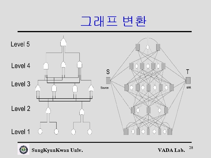 그래프 변환 Sung. Kyun. Kwan Univ. VADA Lab. 28
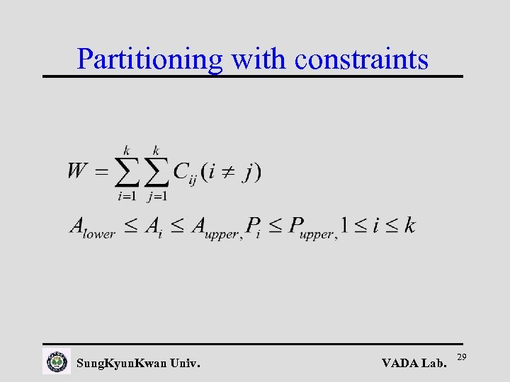 Partitioning with constraints Sung. Kyun. Kwan Univ. VADA Lab. 29
 Algorithm Input: Flow f, Network Output: Partition the network into f subnetworks 단계 1: 그래프에 Flow 를 push하여 최소비용흐름 알고리즘 수행; 만약 각각의 partition에 대하여 A_upper 또는 P_upper를 만족하면 마침; 그렇지않으면 f = f+1; 증가시키고 upper bound를 만족할 때까지 단계 1을 반복한다. 단계 2: 만약 A_lower 또는 P_lower를 만족하지 않는두개의 partition p, q 가 있고 라면 p와 q는 merge가 가능하고 모든 가능한{p, q} set에 대하여 최소비용매칭을 적용 하여 분할된 partition의 개수를 줄임. Sung. Kyun. Kwan Univ. VADA Lab. 30
![참고문헌 [1] J. D. Cho and P. D. Franzon, 참고문헌 [1] J. D. Cho and P. D. Franzon,](https://present5.com/presentation/9bfb1ca58853ea7141bd5ec1866f8ba3/image-31.jpg) 참고문헌 [1] J. D. Cho and P. D. Franzon, "High-Performance Design Automation for Multi-Chip Modules and Packages", World Scientific Pub. Co. 1996 [2] H. J. M. Veendrick, "Short-Circuit Dessipation of Static CMOS Circuitry and its Impact on the Design of Buffer Circuits" IEEE JSSCC, pp. 468 -473, August, 1984 [3] H. B. Bakoglu, "Circuits, Interconnections and Packaging for VLSI", pp. 81 -112, Addison-Wesley Publishing Co. , 1990 [4] K. M. hall. "An r-dimensional quadratic placement algorithm", Management Sci. , vol. 17, pp. 219 -229, Nov, 1970 [5] Cadence Design Systems. "A Vision for Multi-Chip Module design in the nineties", Tech. Rep. Cadence Design Systems Inc. , Santa Clara, CA, 1993 [6] R. Raghavan, J. Cohoon, and S. Shani. "Single Bend Wiring", Journal of Algorithms, 7(2): 232 -257, June, 1986 [7] Kernighan, B. W. and S. lin. "An efficient heuristic procedure to partition graphs" Bell System Technical Journal, 492: 291 -307, Feb. 1970 [8] Wei, Y. C. and C. K. Cheng "Ratio-Cut Partitioning for Hierachical Designs", IEEE Trans. on Computer. Aided Design. 40(7): 911 -921, 1991 [9] S. W. Hadley, B. L. Mark, and A. Vanelli, "An Efficient Eigenvector Approach for Finding Netlist Partitions", IEEE Trans. on Computer-Aided Design, vol. CAD-11, pp. 85 -892, July, 1992 [10] L. R. Fold, Jr. and D. R. Fulkerson. "Flows in Networks", Princeton University Press, Princeton, NJ, 1962 [11] Liu H. and D. F. Wong, "Network Flow Based Multi-Way Partitioning With Area and Pin Constraints", IEEE/ACM Symposium on Physical Design, pp. 12 -17, 1997 [12] Kirkpatrick, S. Jr. , C. Gelatt, and M. Vecchi. "Optimization by simulated annealing", Science, 220(4598): 498 -516, May, 1983 [13] Pedram, M. "Power Minimization in IC Design: Principles and Applications, " ACM Trans. on Design Automation of Electronics Systems, 1(1), Jan. pp. 3 -56, 1996. [14] A. H. Farrahi and M. Sarrafzadeh. "FPGA Technology Mapping for Power Minimizatioin", In International Workshop on Field-Programmable Logic and Applications, pp 66 -77, Sep. 1994 [15] M. A. Breur, "Min-Cut Placement", J. Design Automation and Fault-Tolerant Computing, pp. 343 -382, Oct. 1977 Sung. Kyun. Kwan Univ. VADA Lab. 31
참고문헌 [1] J. D. Cho and P. D. Franzon, "High-Performance Design Automation for Multi-Chip Modules and Packages", World Scientific Pub. Co. 1996 [2] H. J. M. Veendrick, "Short-Circuit Dessipation of Static CMOS Circuitry and its Impact on the Design of Buffer Circuits" IEEE JSSCC, pp. 468 -473, August, 1984 [3] H. B. Bakoglu, "Circuits, Interconnections and Packaging for VLSI", pp. 81 -112, Addison-Wesley Publishing Co. , 1990 [4] K. M. hall. "An r-dimensional quadratic placement algorithm", Management Sci. , vol. 17, pp. 219 -229, Nov, 1970 [5] Cadence Design Systems. "A Vision for Multi-Chip Module design in the nineties", Tech. Rep. Cadence Design Systems Inc. , Santa Clara, CA, 1993 [6] R. Raghavan, J. Cohoon, and S. Shani. "Single Bend Wiring", Journal of Algorithms, 7(2): 232 -257, June, 1986 [7] Kernighan, B. W. and S. lin. "An efficient heuristic procedure to partition graphs" Bell System Technical Journal, 492: 291 -307, Feb. 1970 [8] Wei, Y. C. and C. K. Cheng "Ratio-Cut Partitioning for Hierachical Designs", IEEE Trans. on Computer. Aided Design. 40(7): 911 -921, 1991 [9] S. W. Hadley, B. L. Mark, and A. Vanelli, "An Efficient Eigenvector Approach for Finding Netlist Partitions", IEEE Trans. on Computer-Aided Design, vol. CAD-11, pp. 85 -892, July, 1992 [10] L. R. Fold, Jr. and D. R. Fulkerson. "Flows in Networks", Princeton University Press, Princeton, NJ, 1962 [11] Liu H. and D. F. Wong, "Network Flow Based Multi-Way Partitioning With Area and Pin Constraints", IEEE/ACM Symposium on Physical Design, pp. 12 -17, 1997 [12] Kirkpatrick, S. Jr. , C. Gelatt, and M. Vecchi. "Optimization by simulated annealing", Science, 220(4598): 498 -516, May, 1983 [13] Pedram, M. "Power Minimization in IC Design: Principles and Applications, " ACM Trans. on Design Automation of Electronics Systems, 1(1), Jan. pp. 3 -56, 1996. [14] A. H. Farrahi and M. Sarrafzadeh. "FPGA Technology Mapping for Power Minimizatioin", In International Workshop on Field-Programmable Logic and Applications, pp 66 -77, Sep. 1994 [15] M. A. Breur, "Min-Cut Placement", J. Design Automation and Fault-Tolerant Computing, pp. 343 -382, Oct. 1977 Sung. Kyun. Kwan Univ. VADA Lab. 31
![[16] M. Hanan and M. J. Kutrzberg. A Review of the Placement and the [16] M. Hanan and M. J. Kutrzberg. A Review of the Placement and the](https://present5.com/presentation/9bfb1ca58853ea7141bd5ec1866f8ba3/image-32.jpg) [16] M. Hanan and M. J. Kutrzberg. A Review of the Placement and the Quadratic Assignment Problem, Apr. 1072. [17] N. R. Quinn, "The Placement Problem as Viewed from the Physics of Classical Mechanics", Proc. of the 12 th Design Automation Conference, pp. 173 -178, 1975 [18] C. Sehen, and A. Sangiovanni-Vincentelli, "The Timber Wolf placement and routing package", IEEE Journal of Solid-State Circuits, Sc-20, pp. 501 -522, 1985 [19] K. Shahookar, and P. Mazumder, "A Genetic Approach to Standard Cell Placement", First European Design Automation Conference, Mar. 1990 [20] J. D. Cho, S. Raje, M. Sarrafzadeh, M. Sriram, and S. M. Kang, "Crosstalk Minimum Layer Assignment", In Proc. IEEE Custom Integr. Circuits Conf. , San Diego, CA, pp. 29. 7. 1 -29. 7. 4, 1993 [21] J. M. Ho, M. Sarrafzadeh, G, Vijayan, and C. K. Wong. "Layer Assignment for Multi-Chip Modules", IEEE Trans. on Computer-Aided Design, CAD-9(12): 1272 -1277, Dec. , 1991 [22] G. Devaraj. "Distributed placement and crosstalk driven router for multichip modules", In MS Thesis, Univ. of Cincinnati, 1994 [23] J. D. Cho. "Min-Cost Flow based Minimum-Cost Rectilinear Steiner Distance-Preserving Tree", International Symposium on Physical Desigh, pp-82 -87, 1997 [24] A. Vitttal and M. Marek-Sadowska. "Minimal Delay Interconnection Design using Alphabetic Trees", In Design Automation Conference, pp. 392 -396, 1994 [25] M. C. Golumbic. "Algorithmic Graph Theory and Perfect Graph", pp. 80 -103, New York : Academic. 1980 [26] R. Vemuri. "Genetic Algorithms for partitioning, placement, and layer assignment for multichip modules", Ph. D. Thesis, Univ. of Cincinnati, 1994 [27] J. L. Kennington and R. V. Helgason, "Algorithms for Network Programmin", John Wiley, 1980 [28] J. Y. Cho and J. D. Cho "Improving Performance and Routability Estimation in MCM Placement", In Inter. Pack'97, Hawaii, June, 1997 [29] J. Y. Cho and J. D. Cho "Partitioning for Low Power Using Min-Cost Flow Algorithm", submitted to 한국반도체학술대회, Feb, 1998 Sung. Kyun. Kwan Univ. VADA Lab. 32
[16] M. Hanan and M. J. Kutrzberg. A Review of the Placement and the Quadratic Assignment Problem, Apr. 1072. [17] N. R. Quinn, "The Placement Problem as Viewed from the Physics of Classical Mechanics", Proc. of the 12 th Design Automation Conference, pp. 173 -178, 1975 [18] C. Sehen, and A. Sangiovanni-Vincentelli, "The Timber Wolf placement and routing package", IEEE Journal of Solid-State Circuits, Sc-20, pp. 501 -522, 1985 [19] K. Shahookar, and P. Mazumder, "A Genetic Approach to Standard Cell Placement", First European Design Automation Conference, Mar. 1990 [20] J. D. Cho, S. Raje, M. Sarrafzadeh, M. Sriram, and S. M. Kang, "Crosstalk Minimum Layer Assignment", In Proc. IEEE Custom Integr. Circuits Conf. , San Diego, CA, pp. 29. 7. 1 -29. 7. 4, 1993 [21] J. M. Ho, M. Sarrafzadeh, G, Vijayan, and C. K. Wong. "Layer Assignment for Multi-Chip Modules", IEEE Trans. on Computer-Aided Design, CAD-9(12): 1272 -1277, Dec. , 1991 [22] G. Devaraj. "Distributed placement and crosstalk driven router for multichip modules", In MS Thesis, Univ. of Cincinnati, 1994 [23] J. D. Cho. "Min-Cost Flow based Minimum-Cost Rectilinear Steiner Distance-Preserving Tree", International Symposium on Physical Desigh, pp-82 -87, 1997 [24] A. Vitttal and M. Marek-Sadowska. "Minimal Delay Interconnection Design using Alphabetic Trees", In Design Automation Conference, pp. 392 -396, 1994 [25] M. C. Golumbic. "Algorithmic Graph Theory and Perfect Graph", pp. 80 -103, New York : Academic. 1980 [26] R. Vemuri. "Genetic Algorithms for partitioning, placement, and layer assignment for multichip modules", Ph. D. Thesis, Univ. of Cincinnati, 1994 [27] J. L. Kennington and R. V. Helgason, "Algorithms for Network Programmin", John Wiley, 1980 [28] J. Y. Cho and J. D. Cho "Improving Performance and Routability Estimation in MCM Placement", In Inter. Pack'97, Hawaii, June, 1997 [29] J. Y. Cho and J. D. Cho "Partitioning for Low Power Using Min-Cost Flow Algorithm", submitted to 한국반도체학술대회, Feb, 1998 Sung. Kyun. Kwan Univ. VADA Lab. 32
 6. Logic Level Design Sung. Kyun. Kwan Univ. VADA Lab. 33
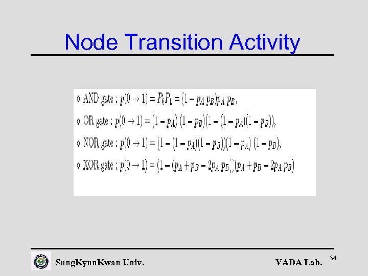 Node Transition Activity Sung. Kyun. Kwan Univ. VADA Lab. 34
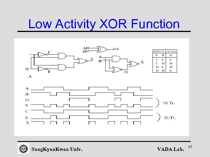 Low Activity XOR Function Sung. Kyun. Kwan Univ. VADA Lab. 35
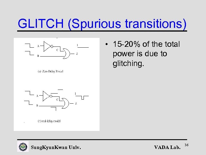 GLITCH (Spurious transitions) • 15 -20% of the total power is due to glitching. Sung. Kyun. Kwan Univ. VADA Lab. 36
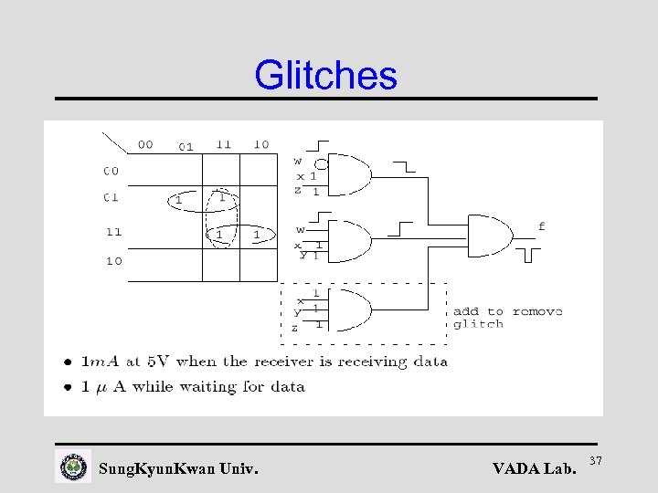 Glitches Sung. Kyun. Kwan Univ. VADA Lab. 37
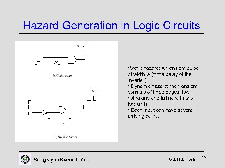 Hazard Generation in Logic Circuits • Static hazard: A transient pulse of width w (= the delay of the inverter). • Dynamic hazard: the transient consists of three edges, two rising and one falling with w of two units. • Each input can have several arriving paths. Sung. Kyun. Kwan Univ. VADA Lab. 38
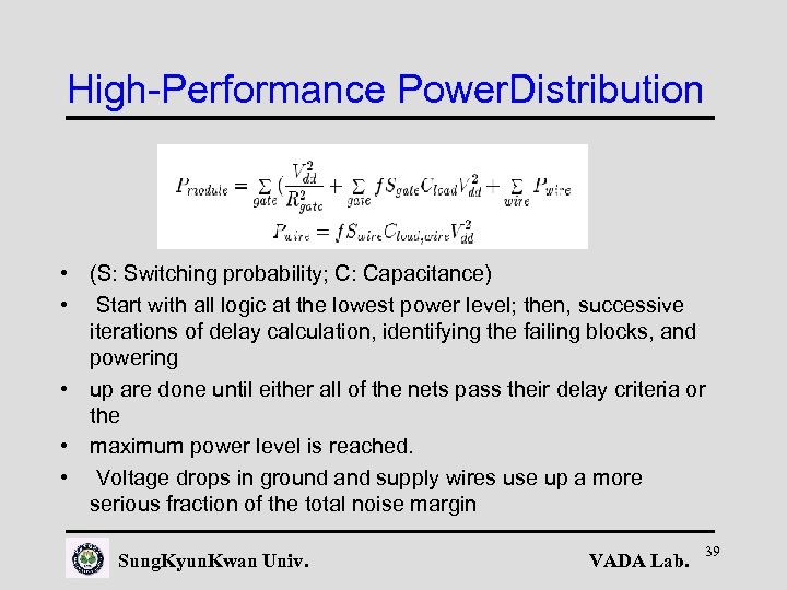 High-Performance Power. Distribution • (S: Switching probability; C: Capacitance) • Start with all logic at the lowest power level; then, successive iterations of delay calculation, identifying the failing blocks, and powering • up are done until either all of the nets pass their delay criteria or the • maximum power level is reached. • Voltage drops in ground and supply wires use up a more serious fraction of the total noise margin Sung. Kyun. Kwan Univ. VADA Lab. 39
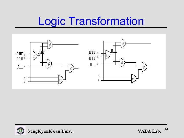
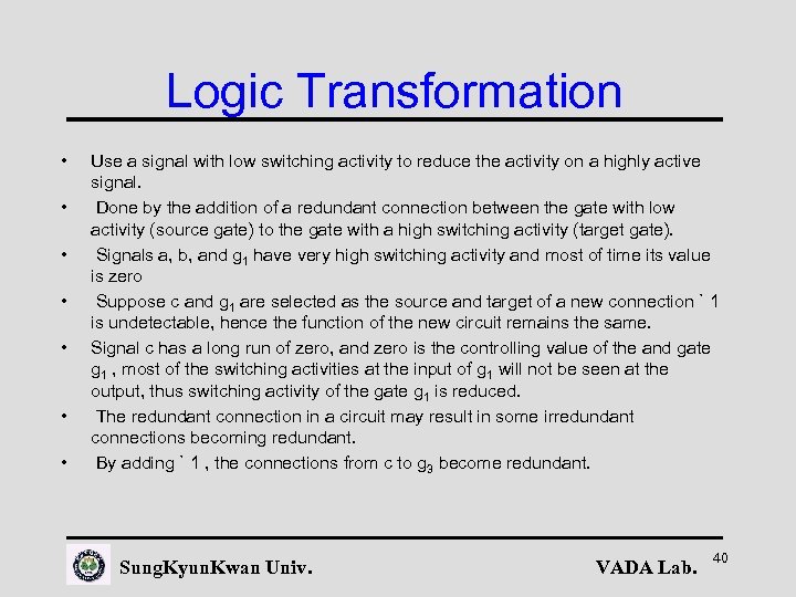 Logic Transformation • • Use a signal with low switching activity to reduce the activity on a highly active signal. Done by the addition of a redundant connection between the gate with low activity (source gate) to the gate with a high switching activity (target gate). Signals a, b, and g 1 have very high switching activity and most of time its value is zero Suppose c and g 1 are selected as the source and target of a new connection ` 1 is undetectable, hence the function of the new circuit remains the same. Signal c has a long run of zero, and zero is the controlling value of the and gate g 1 , most of the switching activities at the input of g 1 will not be seen at the output, thus switching activity of the gate g 1 is reduced. The redundant connection in a circuit may result in some irredundant connections becoming redundant. By adding ` 1 , the connections from c to g 3 become redundant. Sung. Kyun. Kwan Univ. VADA Lab. 40
 Logic Transformation Sung. Kyun. Kwan Univ. VADA Lab. 41
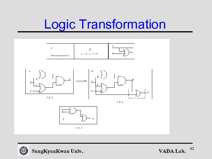 Logic Transformation Sung. Kyun. Kwan Univ. VADA Lab. 42
 Frequency Reduction ◈ Power saving 4 Reduces capacitance on the clock network 4 Reduces internal power in the affected registers 4 Reduces need for muxes(data recirculation) ◈ Opportunity 4 Large opportunity for power reduction, dependent on; · Number of registers gated · percentage of time clock is enabled ◈ Cost 4 Testability 4 Complicates clock tree synthesis 4 Complicates clock skew balancing Sung. Kyun. Kwan Univ. VADA Lab. 43
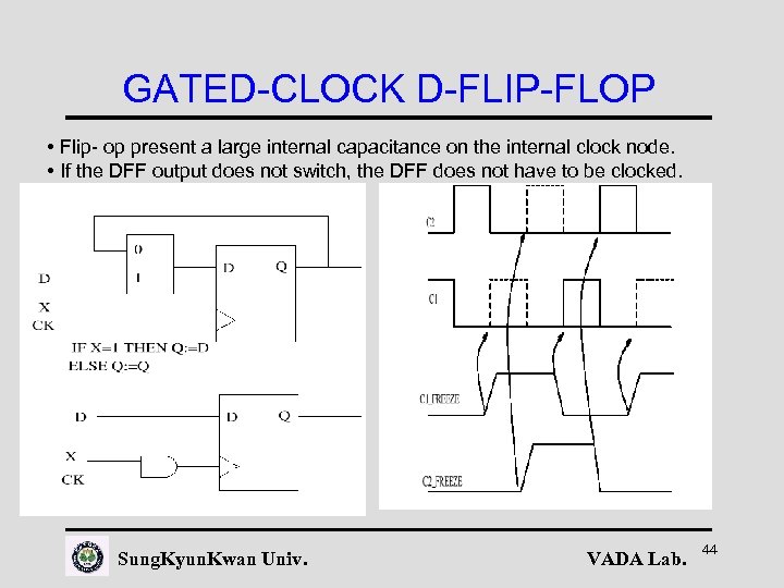 GATED-CLOCK D-FLIP-FLOP • Flip- op present a large internal capacitance on the internal clock node. • If the DFF output does not switch, the DFF does not have to be clocked. Sung. Kyun. Kwan Univ. VADA Lab. 44
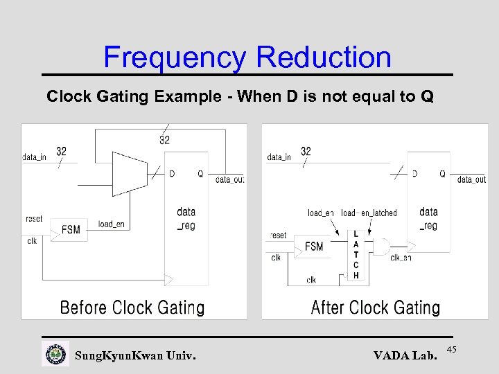 Frequency Reduction Clock Gating Example - When D is not equal to Q Sung. Kyun. Kwan Univ. VADA Lab. 45
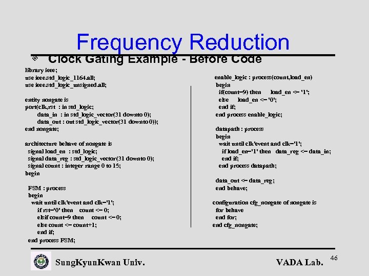 Frequency Reduction ◈ Clock Gating Example - Before Code library ieee; use ieee. std_logic_1164. all; use ieee. std_logic_unsigned. all; entity nongate is port(clk, rst : in std_logic; data_in : in std_logic_vector(31 downto 0); data_out : out std_logic_vector(31 downto 0)); end nongate; architecture behave of nongate is signal load_en : std_logic; signal data_reg : std_logic_vector(31 downto 0); signal count : integer range 0 to 15; begin FSM : process begin wait until clk'event and clk='1'; if rst='0' then count <= 0; elsif count=9 then count <= 0; else count <= count+1; end if; end process FSM; Sung. Kyun. Kwan Univ. enable_logic : process(count, load_en) begin if(count=9) then load_en <= '1'; else load_en <= '0'; end if; end process enable_logic; datapath : process begin wait until clk'event and clk='1'; if load_en='1' then data_reg <= data_in; end if; end process datapath; data_out <= data_reg; end behave; configuration cfg_nongate of nongate is for behave end for; end cfg_nongate; VADA Lab. 46
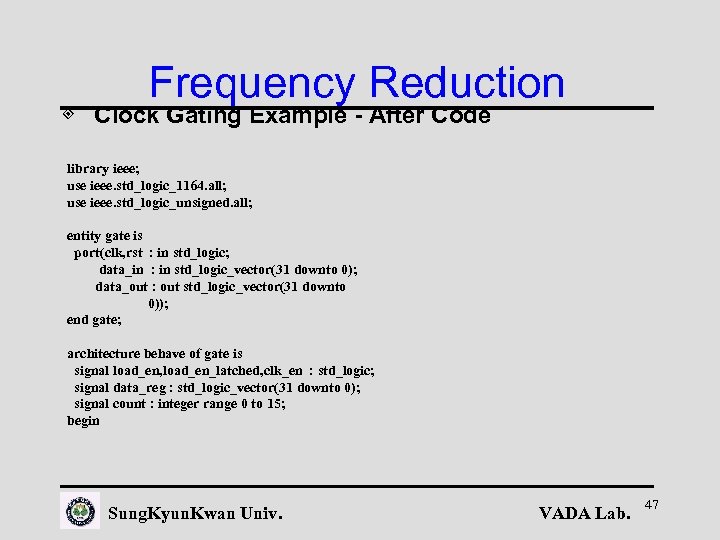 Frequency Reduction ◈ Clock Gating Example - After Code library ieee; use ieee. std_logic_1164. all; use ieee. std_logic_unsigned. all; entity gate is port(clk, rst : in std_logic; data_in : in std_logic_vector(31 downto 0); data_out : out std_logic_vector(31 downto 0)); end gate; architecture behave of gate is signal load_en, load_en_latched, clk_en : std_logic; signal data_reg : std_logic_vector(31 downto 0); signal count : integer range 0 to 15; begin Sung. Kyun. Kwan Univ. VADA Lab. 47
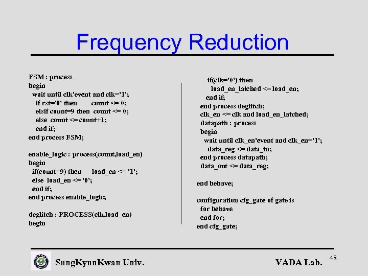 Frequency Reduction FSM : process begin wait until clk'event and clk='1'; if rst='0' then count <= 0; elsif count=9 then count <= 0; else count <= count+1; end if; end process FSM; enable_logic : process(count, load_en) begin if(count=9) then load_en <= '1'; else load_en <= '0'; end if; end process enable_logic; deglitch : PROCESS(clk, load_en) begin Sung. Kyun. Kwan Univ. if(clk='0') then load_en_latched <= load_en; end if; end process deglitch; clk_en <= clk and load_en_latched; datapath : process begin wait until clk_en'event and clk_en='1'; data_reg <= data_in; end process datapath; data_out <= data_reg; end behave; configuration cfg_gate of gate is for behave end for; end cfg_gate; VADA Lab. 48
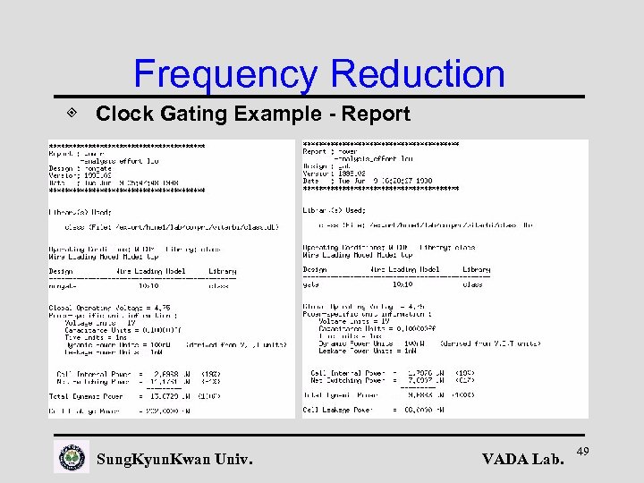 Frequency Reduction ◈ Clock Gating Example - Report Sung. Kyun. Kwan Univ. VADA Lab. 49
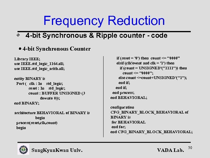 Frequency Reduction ◈ 4 -bit Synchronous & Ripple counter - code 4 -bit Synchronous Counter Library IEEE; use IEEE. std_logic_1164. all; use IEEE. std_logic_arith. all; entity BINARY is Port ( clk : In std_logic; reset : In std_logic; count : BUFFER UNSIGNED (3 downto 0)); end BINARY; architecture BEHAVIORAL of BINARY is begin process(reset, clk, count) begin Sung. Kyun. Kwan Univ. if (reset = '0') then count <= "0000” elsif (clk'event and clk = '1') then if (count = UNSIGNED'("1111")) then count <= "0000"; else count <=count+UNSIGNED'("1"); end if; end process; end BEHAVIORAL; configuration CFG_BINARY_BLOCK_BEHAVIORAL of BINARY is for BEHAVIORAL end for; end CFG_BINARY_BLOCK_BEHAVIORAL; VADA Lab. 50
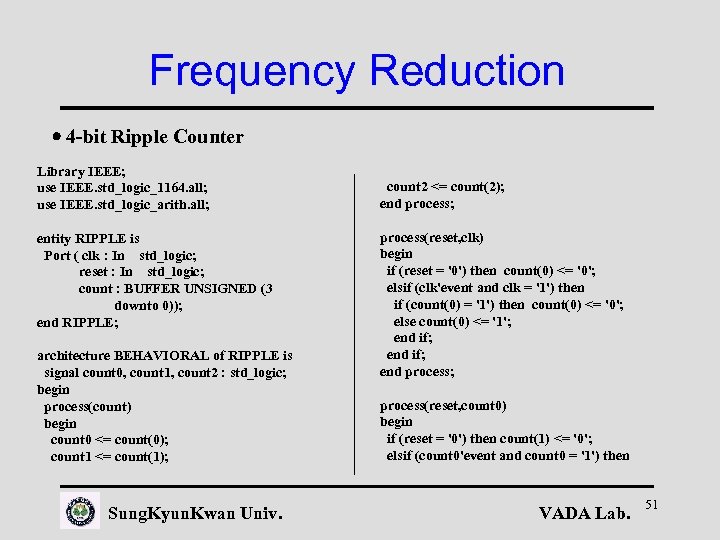 Frequency Reduction 4 -bit Ripple Counter Library IEEE; use IEEE. std_logic_1164. all; use IEEE. std_logic_arith. all; entity RIPPLE is Port ( clk : In std_logic; reset : In std_logic; count : BUFFER UNSIGNED (3 downto 0)); end RIPPLE; architecture BEHAVIORAL of RIPPLE is signal count 0, count 1, count 2 : std_logic; begin process(count) begin count 0 <= count(0); count 1 <= count(1); Sung. Kyun. Kwan Univ. count 2 <= count(2); end process; process(reset, clk) begin if (reset = '0') then count(0) <= '0'; elsif (clk'event and clk = '1') then if (count(0) = '1') then count(0) <= '0'; else count(0) <= '1'; end if; end process; process(reset, count 0) begin if (reset = '0') then count(1) <= '0'; elsif (count 0'event and count 0 = '1') then VADA Lab. 51
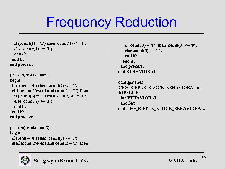 Frequency Reduction if (count(1) = '1') then count(1) <= '0'; else count(1) <= '1'; end if; end process; process(reset, count 1) begin if (reset = '0') then count(2) <= '0'; elsif (count 1'event and count 1 = '1') then if (count(2) = '1') then count(2) <= '0'; else count(2) <= '1'; end if; end process; if (count(3) = '1') then count(3) <= '0'; else count(3) <= '1'; end if; end process; end BEHAVIORAL; configuration CFG_RIPPLE_BLOCK_BEHAVIORAL of RIPPLE is for BEHAVIORAL end for; end CFG_RIPPLE_BLOCK_BEHAVIORAL; process(reset, count 2) begin if (reset = '0') then count(3) <= '0'; elsif (count 2'event and count 2 = '1') then Sung. Kyun. Kwan Univ. VADA Lab. 52
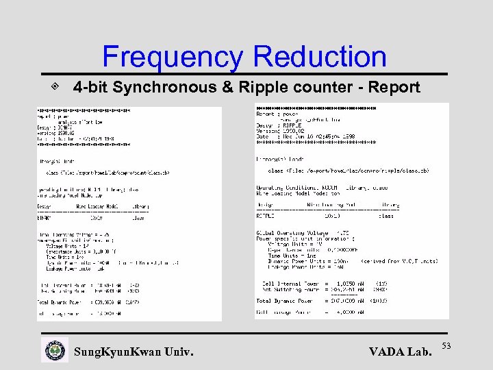 Frequency Reduction ◈ 4 -bit Synchronous & Ripple counter - Report Sung. Kyun. Kwan Univ. VADA Lab. 53
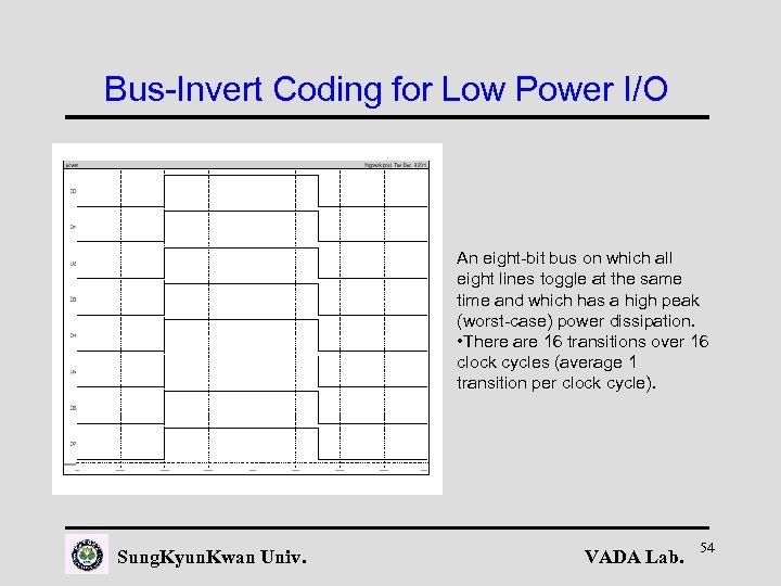 Bus-Invert Coding for Low Power I/O An eight-bit bus on which all eight lines toggle at the same time and which has a high peak (worst-case) power dissipation. • There are 16 transitions over 16 clock cycles (average 1 transition per clock cycle). Sung. Kyun. Kwan Univ. VADA Lab. 54
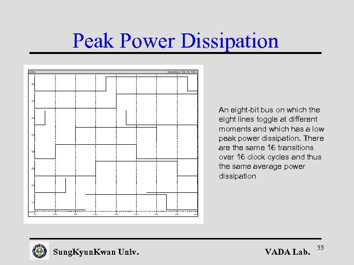 Peak Power Dissipation An eight-bit bus on which the eight lines toggle at different moments and which has a low peak power dissipation. There are the same 16 transitions over 16 clock cycles and thus the same average power dissipation Sung. Kyun. Kwan Univ. VADA Lab. 55
 Bus-Invert - Coding for low power • • • The Bus-Invert method proposed here uses one extra control bit called invert. By convention then invert = 0 the bus value will equal the data value. When invert = 1 the bus value will be the inverted data value. The peak power dissipation can then be decreased by half by coding the I/O as follow 1. Compute the Hamming distance (the number of bits in which they differ) between the present bus value (also counting the present invert line) and the next data value. 2. If the Hamming distance is larger than n=2, set invert = 1 (and thus make the next bus value equal to the inverted next data value). 3. Otherwise, let invert = 0 (and let the next bus value equal to the next data value). 4. At the receiver side the contents of the bus must be conditionally inverted according to the invert line, unless the data is not stored encoded as it is (e. g. in a RAM). In any case the value of invert must be transmitted over the bus (the method increases the number of bus lines from n to n + 1). Sung. Kyun. Kwan Univ. VADA Lab. 56
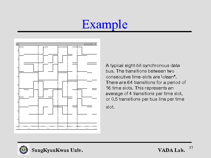 Example A typical eight-bit synchronous data bus. The transitions between two consecutive time-slots are clean". There are 64 transitions for a period of 16 time slots. This represents an average of 4 transitions per time slot, or 0. 5 transitions per bus line per time slot. Sung. Kyun. Kwan Univ. VADA Lab. 57
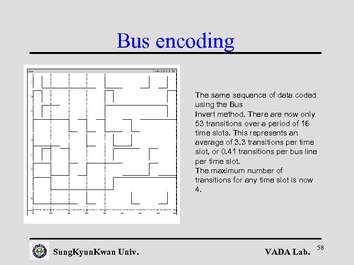 Bus encoding The same sequence of data coded using the Bus Invert method. There are now only 53 transitions over a period of 16 time slots. This represents an average of 3. 3 transitions per time slot, or 0. 41 transitions per bus line per time slot. The maximum number of transitions for any time slot is now 4. Sung. Kyun. Kwan Univ. VADA Lab. 58
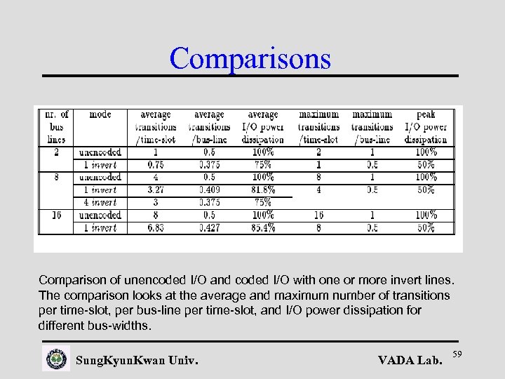 Comparisons Comparison of unencoded I/O and coded I/O with one or more invert lines. The comparison looks at the average and maximum number of transitions per time-slot, per bus-line per time-slot, and I/O power dissipation for different bus-widths. Sung. Kyun. Kwan Univ. VADA Lab. 59
 Remarks • • The increase in the delay of the data-path: By looking at the power-delay product which removes the effect of frequency (delay) on power dissipation, a clear improvement is obtained in the form of an absolute lower number of transitions. It is also relatively easy to pipeline the bus activity. The extra pipeline stage and the extra latency must then be considered. The increased number of I/O pins. As was mentioned before ground-bounce is a big problem for simultaneous switching in high speed designs. That is why modern microprocessors use a large number of Vdd and GND pins. The Bus. Invert method has the side-effect of decreasing the maximum ground-bounce by approximately 50%. Thus circuits using the Bus Invert method can use a lower number of Vdd and GND pins and by using the method the total number of pins might even decrease. Bus-Invert method decreases the total power dissipation although both the total number of transitions increases (by counting the extra internal transitions) and the total capacitance increases (because of the extra circuitry). This is possible because the transitions get redistributed very nonuniformly, more on the low-capacitance side and less on the high-capacitance side. Sung. Kyun. Kwan Univ. VADA Lab. 60
![References [1] H. B. Bakoglu, Circuits, Interconnections and Packaging for VLSI, Addison-Wesley, 1990. [2] References [1] H. B. Bakoglu, Circuits, Interconnections and Packaging for VLSI, Addison-Wesley, 1990. [2]](https://present5.com/presentation/9bfb1ca58853ea7141bd5ec1866f8ba3/image-61.jpg) References [1] H. B. Bakoglu, Circuits, Interconnections and Packaging for VLSI, Addison-Wesley, 1990. [2] T. K. Callaway, E. E. Swartzlander, Estimating the Power Consumption of CMOS Adders", 11 th Symp. on Comp. Arithmetic, pp. 210 -216, Windsor, Ontario, 1993. [3] A. P. Chandrakasan, S. Sheng, R. W. Brodersen, Low-Power CMOS Digital Design", IEEE Journal of Solid-State Circuits, pp. 473 -484, April 1992. [4] A. P. Chandrakasan, M. Potkonjak, J. Rabaey, R. W. Brodersen, HYPER-LP: A System for Power Minimization Using Architectural Transformations", ICCAD-92, pp. 300 -303, Nov. 1992, Santa Clara, CA. [5] A. P. Chandrakasan, M. Potkonjak, J. Rabaey, R. W. Brodersen, An Approach to Power Minimization Using Transformations", IEEE VLSI for Signal Processing Workshop, pp. , 1992, CA. [6] S. Devadas, K. Keutzer, J. White, Estimation of Power Dissipation in CMOS Combinational Circuits", IEEE Custom Integrated Circuits Conference, pp. 19. 7. 1 -19. 7. 6, 1990. [7] D. Dobberpuhl et al. A 200 -MHz 64 -bit Dual-Issue CMOS Microprocessor", IEEE Journal of Solid-State Circuits, pp. 15551567, Nov. 1992. [8] R. J. Fletcher, Integrated Circuit Having Outputs Congured for Reduced State Changes", U. S. Patent no. 4, 667, 337, May, 1987. Sung. Kyun. Kwan Univ. [9] D. Gajski, N. Dutt, A. Wu, S. Lin, High-Level Synthesis, Introduction to Chip and System Design, Kluwer Academic Publishers, 1992. [10] J. S. Gardner, Designing with the IDT Sync. FIFO: the Architecture of the Future", 1992 Synchronous (Clocked) FIFO Design Guide, Integrated Device Technology AN-60, pp. 7 -10, 1992, Santa Clara, CA. [11] A. Ghosh, S. Devadas, K. Keutzer, J. White, Estimation of Average Switching Activity in Combinational and Sequential Circuits", Proceedings of the 29 th DAC, pp. 253 -259, June 1992, Anaheim, CA. [12] J. L. Hennessy, D. A. Patterson, Computer Architecture - A Quantitative Approach, Morgan Kaufmann Publishers, Palo Alto, CA, 1990. [13] S. Kodical, Simultaneous Switching Noise", 1993 IDT High-Speed CMOS Logic Design Guide, Integrated Device Technology AN-47, pp. 41 -47, 1993, Santa Clara, CA. [14] F. Najm, Transition Density, A Stochastic Measure of Activity in Digital Circuits", Proceedings of the 28 th DAC, pp. 644 -649, June 1991, Anaheim, CA. VADA Lab. 61
References [1] H. B. Bakoglu, Circuits, Interconnections and Packaging for VLSI, Addison-Wesley, 1990. [2] T. K. Callaway, E. E. Swartzlander, Estimating the Power Consumption of CMOS Adders", 11 th Symp. on Comp. Arithmetic, pp. 210 -216, Windsor, Ontario, 1993. [3] A. P. Chandrakasan, S. Sheng, R. W. Brodersen, Low-Power CMOS Digital Design", IEEE Journal of Solid-State Circuits, pp. 473 -484, April 1992. [4] A. P. Chandrakasan, M. Potkonjak, J. Rabaey, R. W. Brodersen, HYPER-LP: A System for Power Minimization Using Architectural Transformations", ICCAD-92, pp. 300 -303, Nov. 1992, Santa Clara, CA. [5] A. P. Chandrakasan, M. Potkonjak, J. Rabaey, R. W. Brodersen, An Approach to Power Minimization Using Transformations", IEEE VLSI for Signal Processing Workshop, pp. , 1992, CA. [6] S. Devadas, K. Keutzer, J. White, Estimation of Power Dissipation in CMOS Combinational Circuits", IEEE Custom Integrated Circuits Conference, pp. 19. 7. 1 -19. 7. 6, 1990. [7] D. Dobberpuhl et al. A 200 -MHz 64 -bit Dual-Issue CMOS Microprocessor", IEEE Journal of Solid-State Circuits, pp. 15551567, Nov. 1992. [8] R. J. Fletcher, Integrated Circuit Having Outputs Congured for Reduced State Changes", U. S. Patent no. 4, 667, 337, May, 1987. Sung. Kyun. Kwan Univ. [9] D. Gajski, N. Dutt, A. Wu, S. Lin, High-Level Synthesis, Introduction to Chip and System Design, Kluwer Academic Publishers, 1992. [10] J. S. Gardner, Designing with the IDT Sync. FIFO: the Architecture of the Future", 1992 Synchronous (Clocked) FIFO Design Guide, Integrated Device Technology AN-60, pp. 7 -10, 1992, Santa Clara, CA. [11] A. Ghosh, S. Devadas, K. Keutzer, J. White, Estimation of Average Switching Activity in Combinational and Sequential Circuits", Proceedings of the 29 th DAC, pp. 253 -259, June 1992, Anaheim, CA. [12] J. L. Hennessy, D. A. Patterson, Computer Architecture - A Quantitative Approach, Morgan Kaufmann Publishers, Palo Alto, CA, 1990. [13] S. Kodical, Simultaneous Switching Noise", 1993 IDT High-Speed CMOS Logic Design Guide, Integrated Device Technology AN-47, pp. 41 -47, 1993, Santa Clara, CA. [14] F. Najm, Transition Density, A Stochastic Measure of Activity in Digital Circuits", Proceedings of the 28 th DAC, pp. 644 -649, June 1991, Anaheim, CA. VADA Lab. 61
![References [16] A. Park, R. Maeder, Codes to Reduce Switching Transients Across VLSI I/O References [16] A. Park, R. Maeder, Codes to Reduce Switching Transients Across VLSI I/O](https://present5.com/presentation/9bfb1ca58853ea7141bd5ec1866f8ba3/image-62.jpg) References [16] A. Park, R. Maeder, Codes to Reduce Switching Transients Across VLSI I/O Pins", Computer Architecture News, pp. 17 -21, Sept. 1992. [17] Rambus - Architectural Overview, Rambus Inc. , Mountain View, CA, 1993. Contact ray@rambus. com. [18] A. Shen, A. Ghosh, S. Devadas, K. Keutzer, On Average Power Dissipation and Random Pattern Testability", ICCAD-92, pp. 402 -407, Nov. 1992, Santa Clara, CA. [19] M. R. Stan, Shift register generators for circular FIFOs", Electronic Engineering, pp. 26 -27, February 1991, Morgan Grampian House, London, England. [20] M. R. Stan, W. P. Burleson, Limited-weight codes for low power I/O", International Workshop on Low Power Design, April 1994, Napa, CA. Sung. Kyun. Kwan Univ. [21] J. Tabor, Noise Reduction Using Low Weight and Constant Weight Coding Techniques, Master's Thesis, EECS Dept. , MIT, May 1990. [22] W. -C. Tan, T. H. -Y. Meng, Low-power polygon renderer for computer graphics", Int. Conf. on A. S. A. P. , pp. 200 -213, 1993. [23] N. Weste, K. Eshraghian, Principles of CMOS VLSI Design, A Systems Perspective, Addison. Wesley Publishing Company, 1988. [24] R. Wilson, Low power and paradox", Electronic Engineering Times, pp. 38, November 1, 1993. [25] J. Ziv, A. Lempel, A universal Algorithm for Sequential Data Compression", IEEE Trans. on Inf. Theory, vol. IT-23, pp. 337 -343, 1977. VADA Lab. 62
References [16] A. Park, R. Maeder, Codes to Reduce Switching Transients Across VLSI I/O Pins", Computer Architecture News, pp. 17 -21, Sept. 1992. [17] Rambus - Architectural Overview, Rambus Inc. , Mountain View, CA, 1993. Contact ray@rambus. com. [18] A. Shen, A. Ghosh, S. Devadas, K. Keutzer, On Average Power Dissipation and Random Pattern Testability", ICCAD-92, pp. 402 -407, Nov. 1992, Santa Clara, CA. [19] M. R. Stan, Shift register generators for circular FIFOs", Electronic Engineering, pp. 26 -27, February 1991, Morgan Grampian House, London, England. [20] M. R. Stan, W. P. Burleson, Limited-weight codes for low power I/O", International Workshop on Low Power Design, April 1994, Napa, CA. Sung. Kyun. Kwan Univ. [21] J. Tabor, Noise Reduction Using Low Weight and Constant Weight Coding Techniques, Master's Thesis, EECS Dept. , MIT, May 1990. [22] W. -C. Tan, T. H. -Y. Meng, Low-power polygon renderer for computer graphics", Int. Conf. on A. S. A. P. , pp. 200 -213, 1993. [23] N. Weste, K. Eshraghian, Principles of CMOS VLSI Design, A Systems Perspective, Addison. Wesley Publishing Company, 1988. [24] R. Wilson, Low power and paradox", Electronic Engineering Times, pp. 38, November 1, 1993. [25] J. Ziv, A. Lempel, A universal Algorithm for Sequential Data Compression", IEEE Trans. on Inf. Theory, vol. IT-23, pp. 337 -343, 1977. VADA Lab. 62
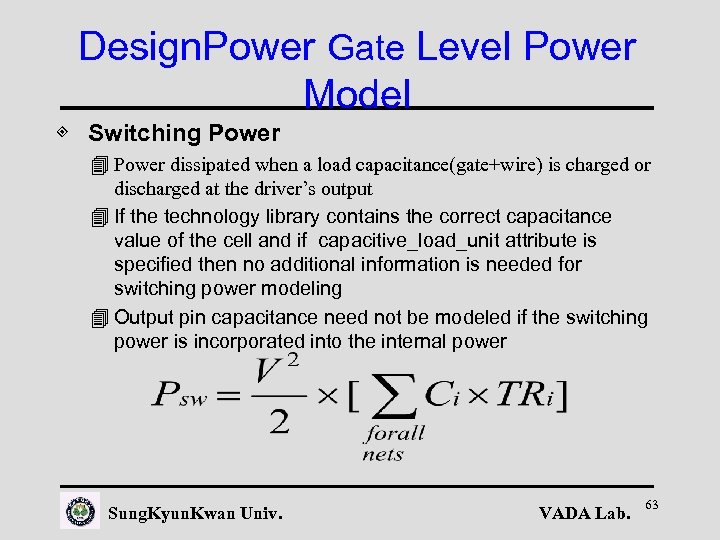 Design. Power Gate Level Power Model ◈ Switching Power 4 Power dissipated when a load capacitance(gate+wire) is charged or discharged at the driver’s output 4 If the technology library contains the correct capacitance value of the cell and if capacitive_load_unit attribute is specified then no additional information is needed for switching power modeling 4 Output pin capacitance need not be modeled if the switching power is incorporated into the internal power Sung. Kyun. Kwan Univ. VADA Lab. 63
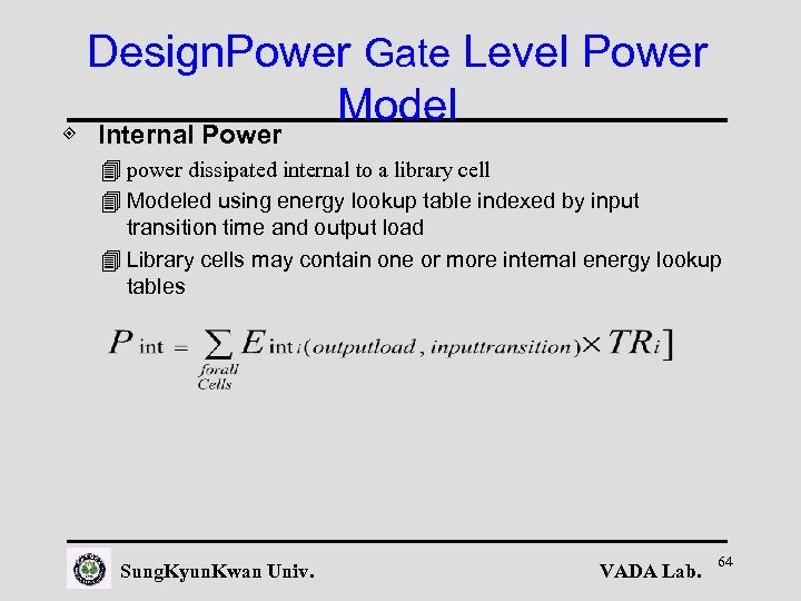 Design. Power Gate Level Power Model ◈ Internal Power 4 power dissipated internal to a library cell 4 Modeled using energy lookup table indexed by input transition time and output load 4 Library cells may contain one or more internal energy lookup tables Sung. Kyun. Kwan Univ. VADA Lab. 64
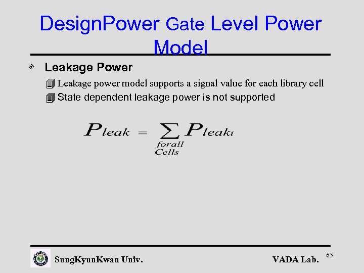 Design. Power Gate Level Power Model ◈ Leakage Power 4 Leakage power model supports a signal value for each library cell 4 State dependent leakage power is not supported Sung. Kyun. Kwan Univ. VADA Lab. 65
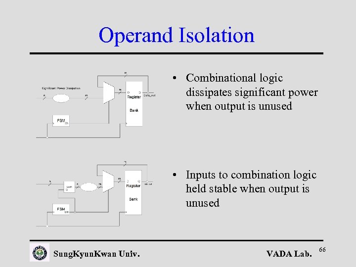 Operand Isolation • Combinational logic dissipates significant power when output is unused • Inputs to combination logic held stable when output is unused Sung. Kyun. Kwan Univ. VADA Lab. 66
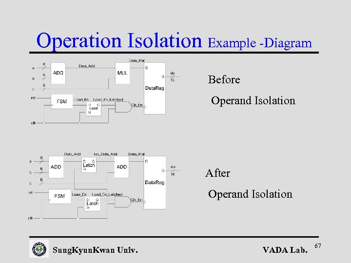 Operation Isolation Example -Diagram Before Operand Isolation After Operand Isolation Sung. Kyun. Kwan Univ. VADA Lab. 67
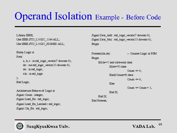 Operand Isolation Example - Before Code Library IEEE; Use IEEE. STD_LOGIC_1164. ALL; Use IEEE. STD_LOGIC_SIGNED. ALL; Signal Data_Add : std_logic_vector(7 downto 0); Signal Data_Mul : std_logic_vector(15 downto 0); Begin Entity Logic is Port( a, b, c : in std_logic_vector(7 downto 0); do : out std_logic_vector(15 downto 0); rst : in std_logic; clk : in std_logic ); End Logic; Process(clk, rst) Architecture Behave of Logic is Signal Count : integer; Signal Load_En : std_logic; Signal Load_En_Latched : std_logic; Signal Clk_En : std_logic; Sung. Kyun. Kwan Univ. -- Counter Logic in FSM Begin If(clk='1' and clk'event) then If(rst='0') then Count <= 0; Elsif(Count=9) then Count <= 0; Else Count <= Count + 1; End If; End Process; VADA Lab. 68
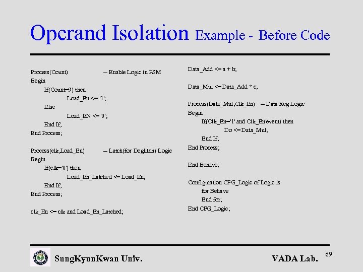 Operand Isolation Example - Before Code Process(Count) -- Enable Logic in FSM Begin If(Count=9) then Load_En <= '1'; Else Load_EN <= '0'; End If; End Process; Process(clk, Load_En) -- Latch(for Deglitch) Logic Begin If(clk='0') then Load_En_Latched <= Load_En; End If; End Process; clk_En <= clk and Load_En_Latched; Sung. Kyun. Kwan Univ. Data_Add <= a + b; Data_Mul <= Data_Add * c; Process(Data_Mul, Clk_En) -- Data Reg Logic Begin If(Clk_En='1' and Clk_En'event) then Do <= Data_Mul; End If; End Process; End Behave; Configuration CFG_Logic of Logic is for Behave End for; End CFG_Logic; VADA Lab. 69
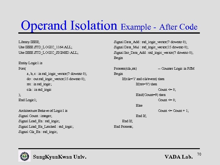 Operand Isolation Example - After Code Library IEEE; Use IEEE. STD_LOGIC_1164. ALL; Use IEEE. STD_LOGIC_SIGNED. ALL; Entity Logic 1 is Port( a, b, c : in std_logic_vector(7 downto 0); do : out std_logic_vector(15 downto 0); rst : in std_logic; clk : in std_logic ); End Logic 1; Architecture Behave of Logic 1 is Signal Count : integer; Signal Load_En : std_logic; Signal Load_En_Latched : std_logic; Signal Clk_En : std_logic; Sung. Kyun. Kwan Univ. Signal Data_Add : std_logic_vector(7 downto 0); Signal Data_Mul : std_logic_vector(15 downto 0); Signal Iso_Data_Add : std_logic_vector(7 downto 0); Begin Process(clk, rst) -- Counter Logic in FSM Begin If(clk='1' and clk'event) then If(rst='0') then Count <= 0; Elsif(Count=9) then Count <= 0; Else Count <= Count + 1; End If; End Process; VADA Lab. 70
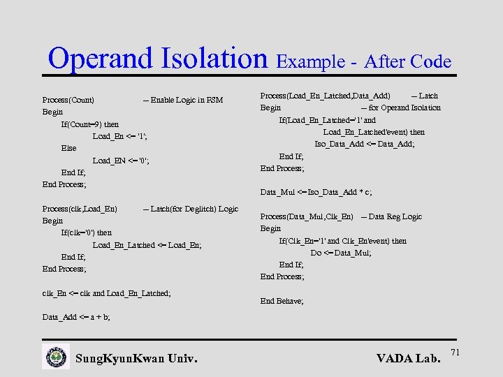 Operand Isolation Example - After Code Process(Count) -- Enable Logic in FSM Begin If(Count=9) then Load_En <= '1'; Else Load_EN <= '0'; End If; End Process; Process(clk, Load_En) -- Latch(for Deglitch) Logic Begin If(clk='0') then Load_En_Latched <= Load_En; End If; End Process; clk_En <= clk and Load_En_Latched; Process(Load_En_Latched, Data_Add) -- Latch Begin -- for Operand Isolation If(Load_En_Latched='1' and Load_En_Latched'event) then Iso_Data_Add <= Data_Add; End If; End Process; Data_Mul <= Iso_Data_Add * c; Process(Data_Mul, Clk_En) -- Data Reg Logic Begin If(Clk_En='1' and Clk_En'event) then Do <= Data_Mul; End If; End Process; End Behave; Data_Add <= a + b; Sung. Kyun. Kwan Univ. VADA Lab. 71
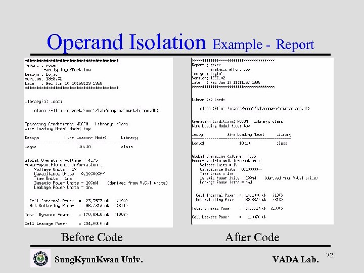 Operand Isolation Example - Report Before Code Sung. Kyun. Kwan Univ. After Code VADA Lab. 72
 Precomputation • Power saving – Reduces power dissipation of combinational logic – Reduces internal power to precomputed registers • Opportunity – Can be significant, dependent on; • percentage of time latch precomputation is successful • Cost – Increase area – Impact circuit timing – Increase design complexity • number of bits to precompute – Testability • may generate redundant logic Sung. Kyun. Kwan Univ. VADA Lab. 73
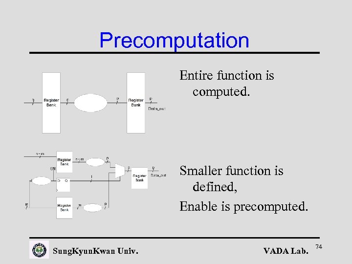 Precomputation Entire function is computed. Smaller function is defined, Enable is precomputed. Sung. Kyun. Kwan Univ. VADA Lab. 74
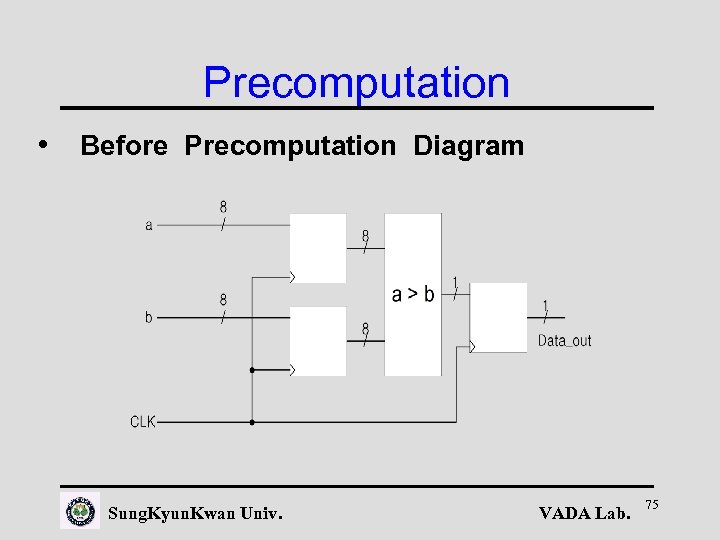 Precomputation • Before Precomputation Diagram Sung. Kyun. Kwan Univ. VADA Lab. 75
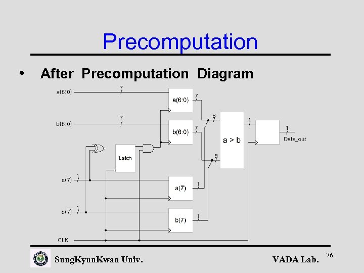 Precomputation • After Precomputation Diagram Sung. Kyun. Kwan Univ. VADA Lab. 76
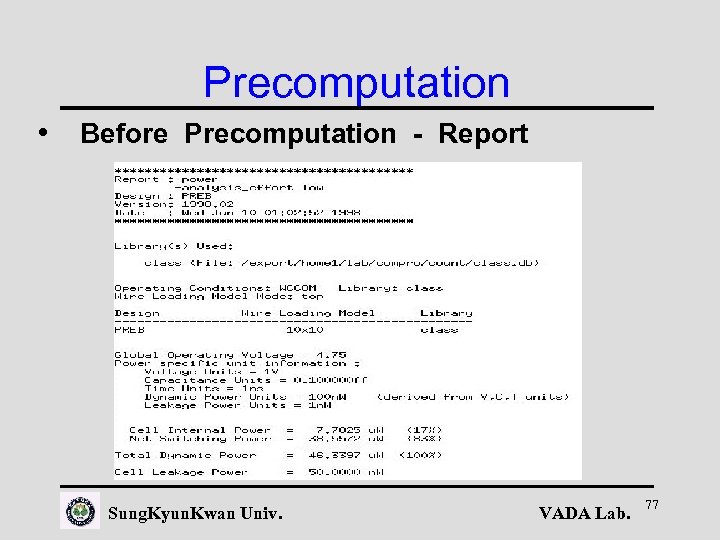 Precomputation • Before Precomputation - Report Sung. Kyun. Kwan Univ. VADA Lab. 77
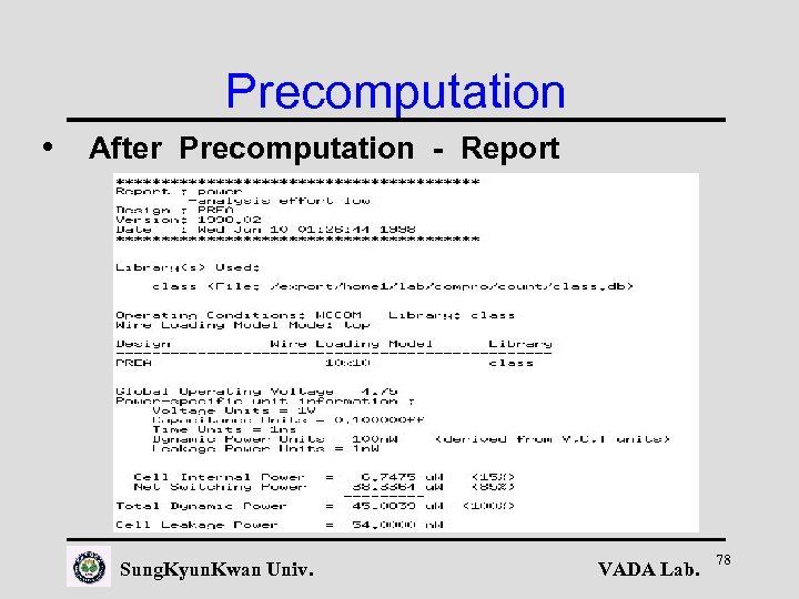 Precomputation • After Precomputation - Report Sung. Kyun. Kwan Univ. VADA Lab. 78
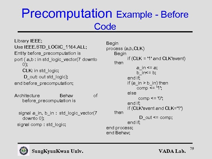 Precomputation Example - Before Code Library IEEE; Use IEEE. STD_LOGIC_1164. ALL; Entity before_precomputation is port ( a, b : in std_logic_vector(7 downto 0); CLK: in std_logic; D_out: out std_logic); end before_precomputation; Architecture Behav before_precomputation is of signal a_in, b_in : std_logic_vector(7 downto 0); signal comp : std_logic; Sung. Kyun. Kwan Univ. Begin process (a, b, CLK) Begin if (CLK = '1' and CLK'event) then a_in <= a; b_in<= b; end if; if (a_in > b_in) then comp <= '1'; else comp <= '0'; end if; if (CLK'event and CLK='1') then D_out <= comp; end if; end process; end Behav; VADA Lab. 79
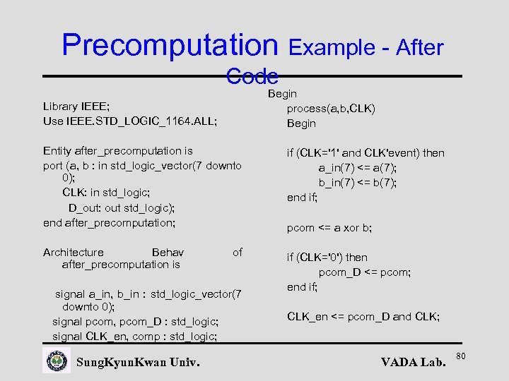 Precomputation Example - After Code Begin process(a, b, CLK) Begin Library IEEE; Use IEEE. STD_LOGIC_1164. ALL; Entity after_precomputation is port (a, b : in std_logic_vector(7 downto 0); CLK: in std_logic; D_out: out std_logic); end after_precomputation; if (CLK='1' and CLK'event) then a_in(7) <= a(7); b_in(7) <= b(7); end if; Architecture Behav after_precomputation is if (CLK='0') then pcom_D <= pcom; end if; of signal a_in, b_in : std_logic_vector(7 downto 0); signal pcom, pcom_D : std_logic; signal CLK_en, comp : std_logic; Sung. Kyun. Kwan Univ. pcom <= a xor b; CLK_en <= pcom_D and CLK; VADA Lab. 80
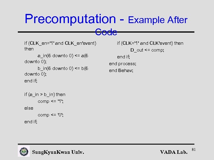 Precomputation - Example After Code if (CLK_en='1' and CLK_en'event) then a_in(6 downto 0) <= a(6 downto 0); b_in(6 downto 0) <= b(6 downto 0); end if; if (CLK='1' and CLK'event) then D_out <= comp; end if; end process; end Behav; if (a_in > b_in) then comp <= '1'; else comp <= '0'; end if; Sung. Kyun. Kwan Univ. VADA Lab. 81
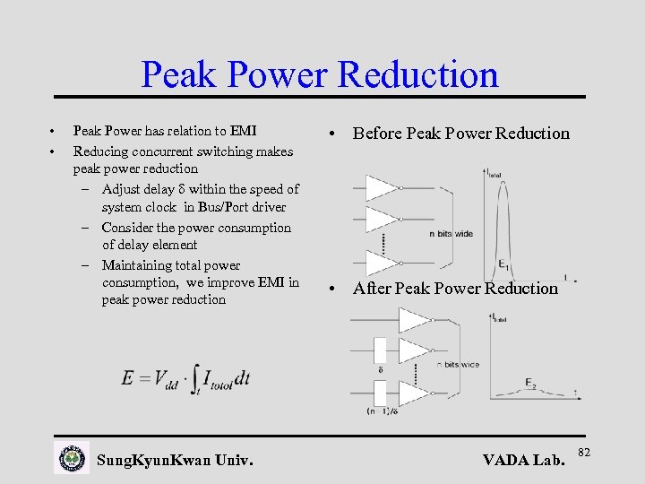 Peak Power Reduction • • Peak Power has relation to EMI Reducing concurrent switching makes peak power reduction – Adjust delay within the speed of system clock in Bus/Port driver – Consider the power consumption of delay element – Maintaining total power consumption, we improve EMI in peak power reduction Sung. Kyun. Kwan Univ. • Before Peak Power Reduction • After Peak Power Reduction VADA Lab. 82
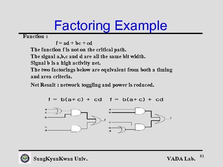 Factoring Example Function : f = ad + bc + cd The function f is not on the critical path. The signal a, b, c and d are all the same bit width. Signal b is a high activity net. The two factorings below are equivalent from both a timing and area criteria. Net Result : network toggling and power is reduced. Sung. Kyun. Kwan Univ. VADA Lab. 83
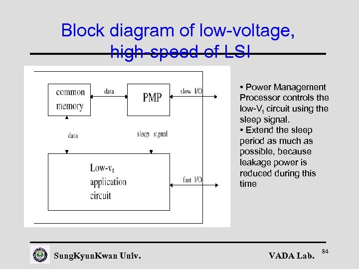 Block diagram of low-voltage, high-speed of LSI • Power Management Processor controls the low-Vt circuit using the sleep signal. • Extend the sleep period as much as possible, because leakage power is reduced during this time Sung. Kyun. Kwan Univ. VADA Lab. 84
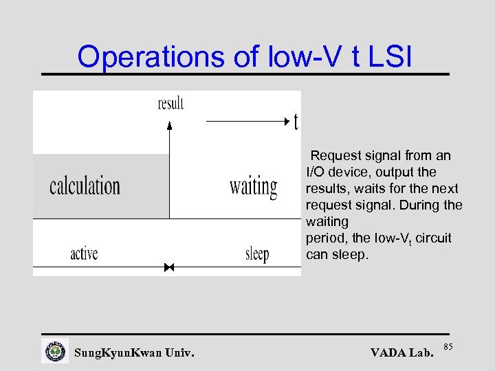 Operations of low-V t LSI Request signal from an I/O device, output the results, waits for the next request signal. During the waiting period, the low-Vt circuit can sleep. Sung. Kyun. Kwan Univ. VADA Lab. 85
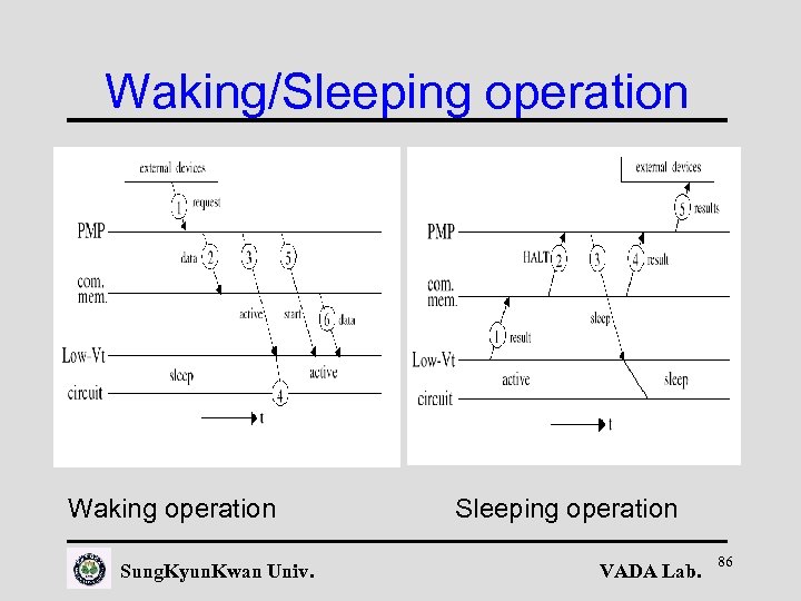 Waking/Sleeping operation Waking operation Sung. Kyun. Kwan Univ. Sleeping operation VADA Lab. 86
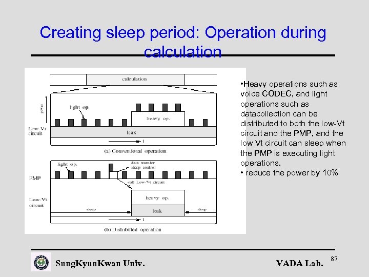 Creating sleep period: Operation during calculation • Heavy operations such as voice CODEC, and light operations such as datacollection can be distributed to both the low-Vt circuit and the PMP, and the low Vt circuit can sleep when the PMP is executing light operations. • reduce the power by 10% Sung. Kyun. Kwan Univ. VADA Lab. 87
 Low Power Logic Gate Resynthesis on Mapped Circuit 김현상 조준동 전기전자컴퓨터공학부 성균관대학교 Sung. Kyun. Kwan Univ. VADA Lab. 88
 Transition Probability • • • Transition Probability: Prob. Of a transition at the output of a gate, given a change at the inputs Use signal probabilities Example: F = X’Y + XY’ – Signal Prob. Of F: Pf = Px(1 -Py)+(1 -Px)Py – Transistion Prob. Of F = 2 Pf(1 -Pf) – Assumption of independence of inputs • • Use BDDs to compute these References: Najm’ 91 Sung. Kyun. Kwan Univ. VADA Lab. 89
 Technology Mapping • Implementing a Boolean network in terms of gates from a given library • Popular technique: Tree-based mapping • Library gates and circuits decomposed into canonical patterns • Pattern matching and dynamic programming to find the best cover • NP-complete for general DAG circuits • Ref: Keutzer’ 87, Rudell’ 89 • Idea: High transition probability points are hidden within gates Sung. Kyun. Kwan Univ. VADA Lab. 90
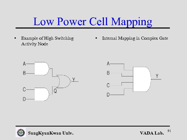 Low Power Cell Mapping • Example of High Switching Activity Node Sung. Kyun. Kwan Univ. • Internal Mapping in Complex Gate VADA Lab. 91
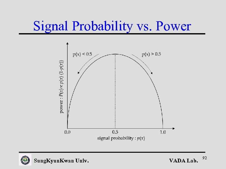 Signal Probability vs. Power Sung. Kyun. Kwan Univ. VADA Lab. 92
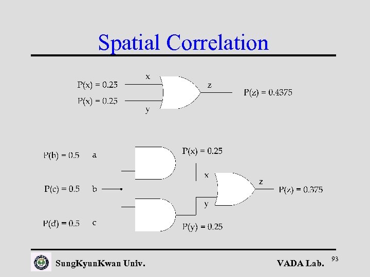 Spatial Correlation Sung. Kyun. Kwan Univ. VADA Lab. 93
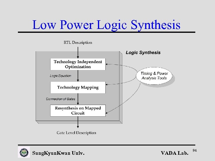 Low Power Logic Synthesis Sung. Kyun. Kwan Univ. VADA Lab. 94
 Technology Mapping Sung. Kyun. Kwan Univ. VADA Lab. 95
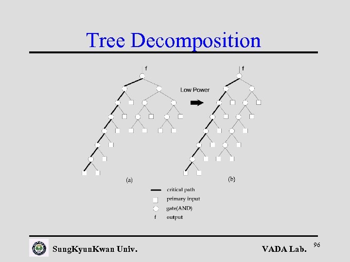 Tree Decomposition Sung. Kyun. Kwan Univ. VADA Lab. 96
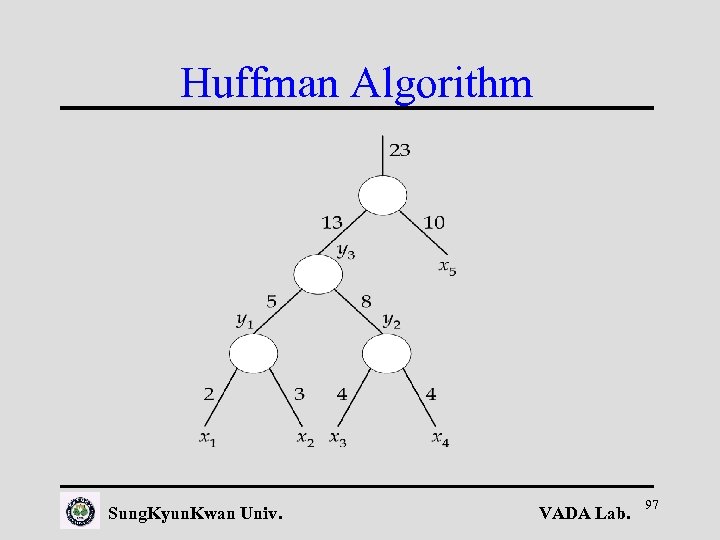 Huffman Algorithm Sung. Kyun. Kwan Univ. VADA Lab. 97
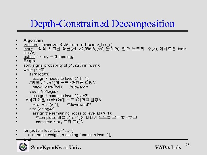 Depth-Constrained Decomposition • • • • • Algorithm problem : minimize SUM from i=1 to m p_t (x_i ) input : 입력 시그널 확률(p 1, p 2, íñíñíñ, pn), 높이(h), 말단 노드의 수(n), 게이트당 fanin limit(k) output : k-ary 트리 topology Begin sort (signal probability of p 1, p 2, íñíñíñ, pn); while (n!=0) if (h>logkn) assign k nodes to level L(=h+1); /*레벨 L(=h+1)에 노드 k개만큼 할당*/ h=h-1, n=n-(k-1); /*upward*/ else if (h
 Example Sung. Kyun. Kwan Univ. VADA Lab. 99
 After Decomposition Sung. Kyun. Kwan Univ. VADA Lab. 100
 After Tech. Mapping Sung. Kyun. Kwan Univ. VADA Lab. 101
 7. Circuit Level Design Sung. Kyun. Kwan Univ. VADA Lab. 102
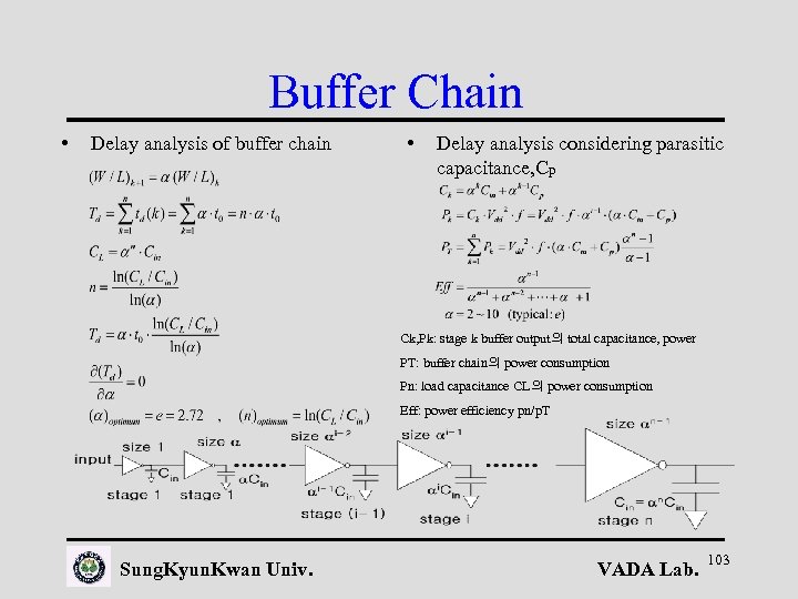 Buffer Chain • Delay analysis of buffer chain • Delay analysis considering parasitic capacitance, Cp Ck, Pk: stage k buffer output의 total capacitance, power PT: buffer chain의 power consumption Pn: load capacitance CL의 power consumption Eff: power efficiency pn/p. T Sung. Kyun. Kwan Univ. VADA Lab. 103
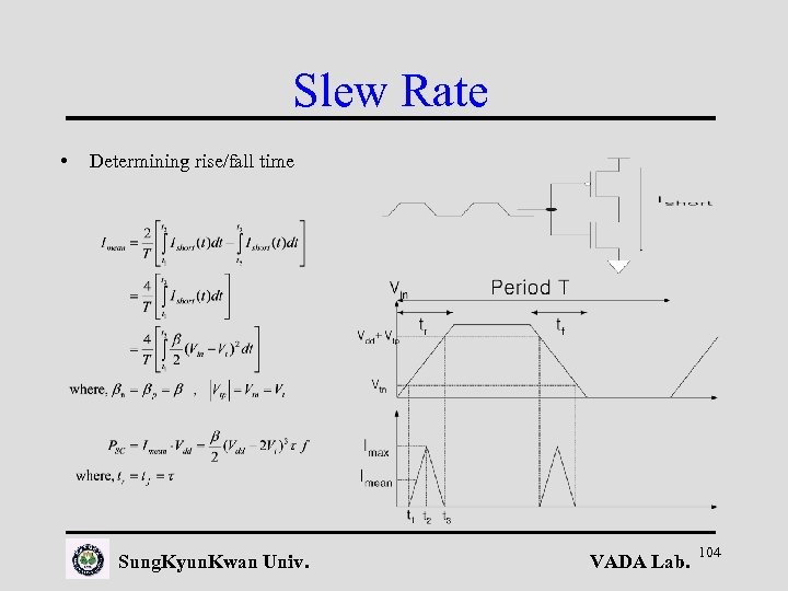 Slew Rate • Determining rise/fall time Sung. Kyun. Kwan Univ. VADA Lab. 104
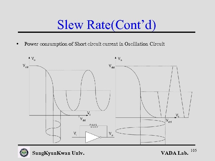 Slew Rate(Cont’d) • Power consumption of Short circuit current in Oscillation Circuit Sung. Kyun. Kwan Univ. VADA Lab. 105
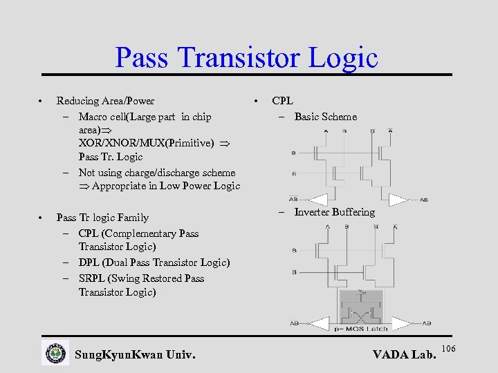 Pass Transistor Logic • Reducing Area/Power – Macro cell(Large part in chip area) XOR/XNOR/MUX(Primitive) Pass Tr. Logic – Not using charge/discharge scheme Appropriate in Low Power Logic • Pass Tr logic Family – CPL (Complementary Pass Transistor Logic) – DPL (Dual Pass Transistor Logic) – SRPL (Swing Restored Pass Transistor Logic) Sung. Kyun. Kwan Univ. • CPL – Basic Scheme – Inverter Buffering VADA Lab. 106
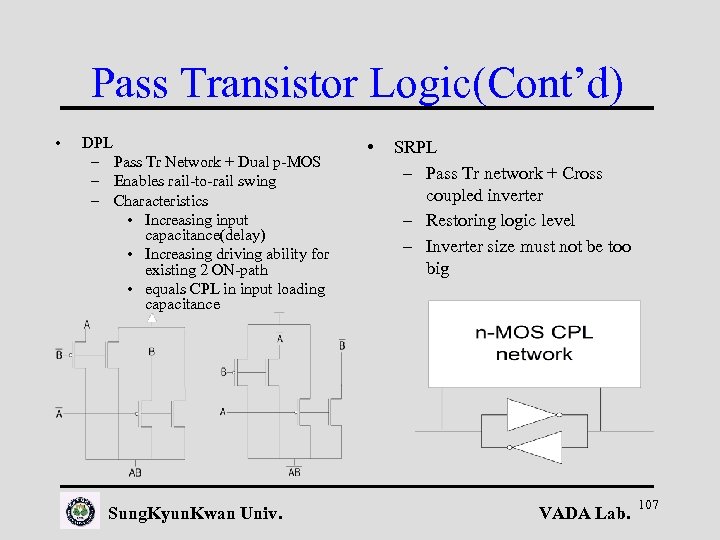 Pass Transistor Logic(Cont’d) • DPL – Pass Tr Network + Dual p-MOS – Enables rail-to-rail swing – Characteristics • Increasing input capacitance(delay) • Increasing driving ability for existing 2 ON-path • equals CPL in input loading capacitance Sung. Kyun. Kwan Univ. • SRPL – Pass Tr network + Cross coupled inverter – Restoring logic level – Inverter size must not be too big VADA Lab. 107
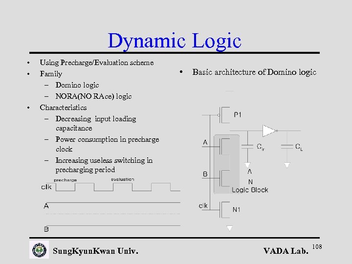 Dynamic Logic • • • Using Precharge/Evaluation scheme Family – Domino logic – NORA(NO RAce) logic Characteristics – Decreasing input loading capacitance – Power consumption in precharge clock – Increasing useless switching in precharging period Sung. Kyun. Kwan Univ. • Basic architecture of Domino logic VADA Lab. 108
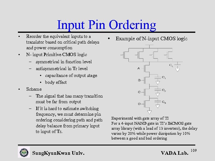 Input Pin Ordering • • • Reorder the equivalent inputs to a transistor based on critical path delays and power consumption N- input Primitive CMOS logic – symmetrical in function level – antisymmetrical in Tr level • capacitance of output stage • body effect Scheme – The signal that has many transition must be far from output – If it is hard to estimate switching frequency, we must determine pin ordering considering path and path delay balance from primary input to input of Tr. Sung. Kyun. Kwan Univ. • Example of N-input CMOS logic Experimentd with gate array of TI For a 4 -input NAND gate in TI’s Bi. CMOS gate array library (with a load of 13 inverters), the delay varies by 20% while power dissipation by 10% between a good and bad ordering VADA Lab. 109
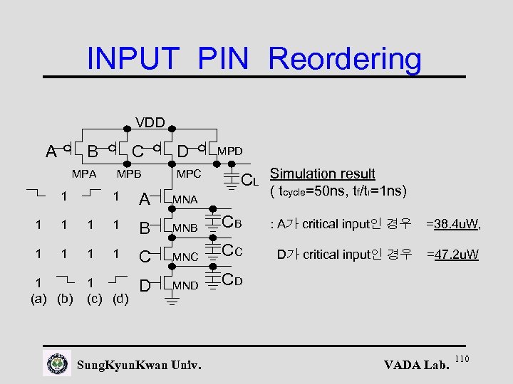 INPUT PIN Reordering VDD A B C MPA MPB 1 D MPC 1 A MPD CL Simulation result ( tcycle=50 ns, tf/tr=1 ns) MNA 1 1 B MNB CB : A가 critical input인 경우 =38. 4 u. W, 1 1 C MNC CC D가 critical input인 경우 =47. 2 u. W D MND CD 1 (a) (b) 1 (c) (d) Sung. Kyun. Kwan Univ. VADA Lab. 110
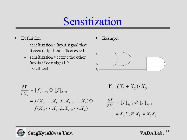 Sensitization • Definition – sensitization : input signal that forces output transition event – sensitization vector : the other inputs if one signal is sensitized Sung. Kyun. Kwan Univ. • Example VADA Lab. 111
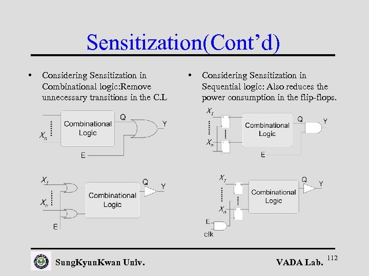 Sensitization(Cont’d) • Considering Sensitization in Combinational logic: Remove unnecessary transitions in the C. L Sung. Kyun. Kwan Univ. • Considering Sensitization in Sequential logic: Also reduces the power consumption in the flip-flops. VADA Lab. 112
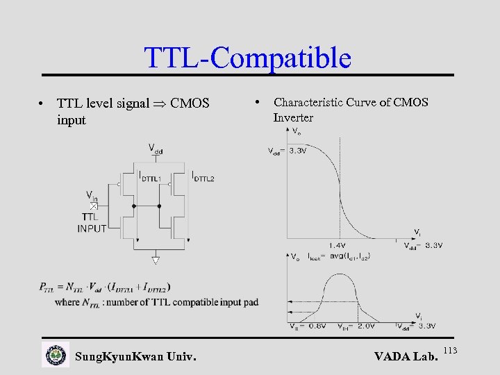 TTL-Compatible • TTL level signal CMOS input Sung. Kyun. Kwan Univ. • Characteristic Curve of CMOS Inverter VADA Lab. 113
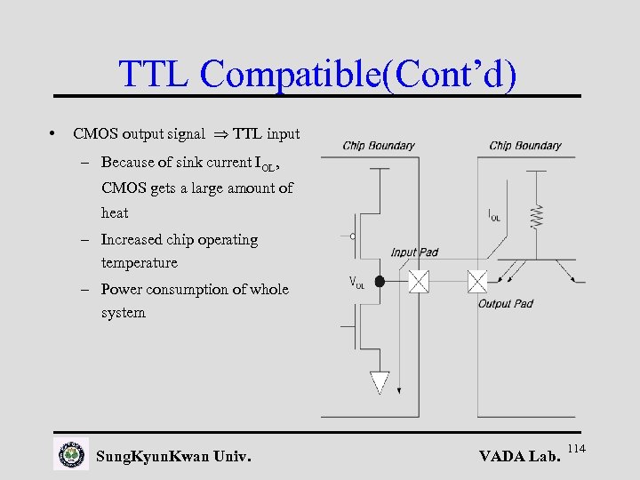 TTL Compatible(Cont’d) • CMOS output signal TTL input – Because of sink current IOL, CMOS gets a large amount of heat – Increased chip operating temperature – Power consumption of whole system Sung. Kyun. Kwan Univ. VADA Lab. 114
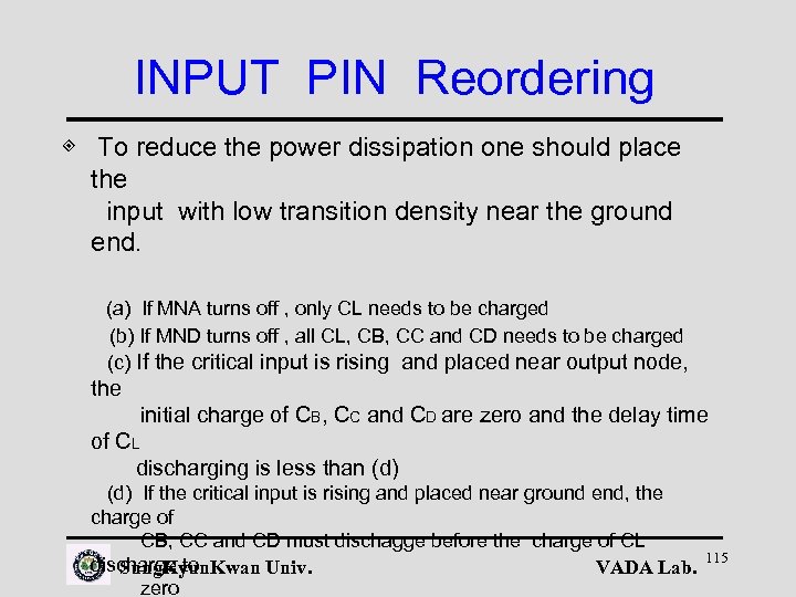 INPUT PIN Reordering ◈ To reduce the power dissipation one should place the input with low transition density near the ground end. (a) If MNA turns off , only CL needs to be charged (b) If MND turns off , all CL, CB, CC and CD needs to be charged (c) If the critical input is rising and placed near output node, the initial charge of CB, CC and CD are zero and the delay time of CL discharging is less than (d) If the critical input is rising and placed near ground end, the charge of CB, CC and CD must dischagge before the charge of CL discharge to Sung. Kyun. Kwan Univ. VADA Lab. zero 115
 저전력 Booth Multiplier 설계 성균관대학교 전기전자컴퓨터공학부 김 진 혁, 이 준 성, 조 준 동 VADA Lab.
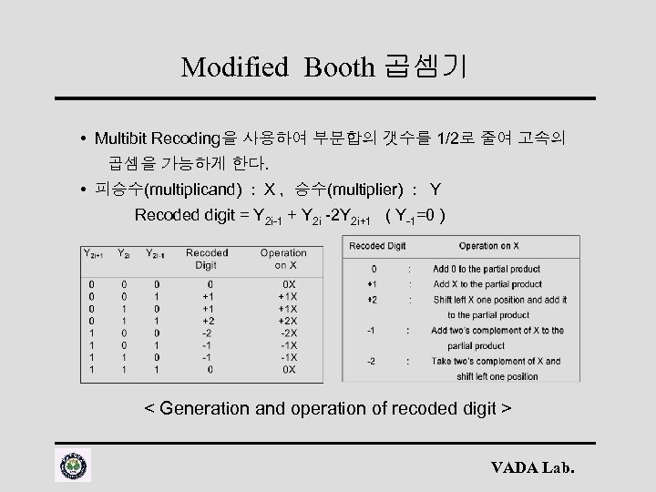 Modified Booth 곱셈기 • Multibit Recoding을 사용하여 부분합의 갯수를 1/2로 줄여 고속의 곱셈을 가능하게 한다. • 피승수(multiplicand) : X , 승수(multiplier) : Y Recoded digit = Y 2 i-1 + Y 2 i -2 Y 2 i+1 ( Y-1=0 ) < Generation and operation of recoded digit > VADA Lab.
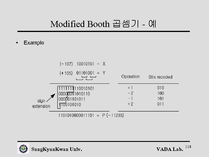 Modified Booth 곱셈기 - 예 • Example Sung. Kyun. Kwan Univ. VADA Lab. 118
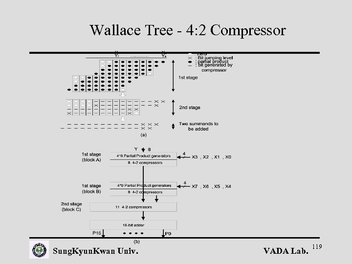 Wallace Tree - 4: 2 Compressor Sung. Kyun. Kwan Univ. VADA Lab. 119
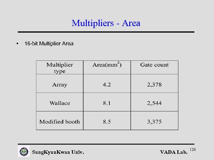 Multipliers - Area • 16 -bit Multiplier Area Sung. Kyun. Kwan Univ. VADA Lab. 120
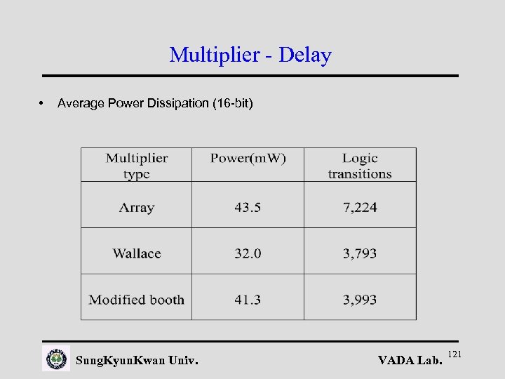 Multiplier - Delay • Average Power Dissipation (16 -bit) Sung. Kyun. Kwan Univ. VADA Lab. 121
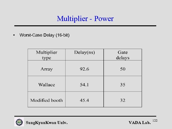 Multiplier - Power • Worst-Case Delay (16 -bit) Sung. Kyun. Kwan Univ. VADA Lab. 122
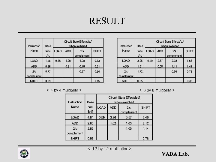
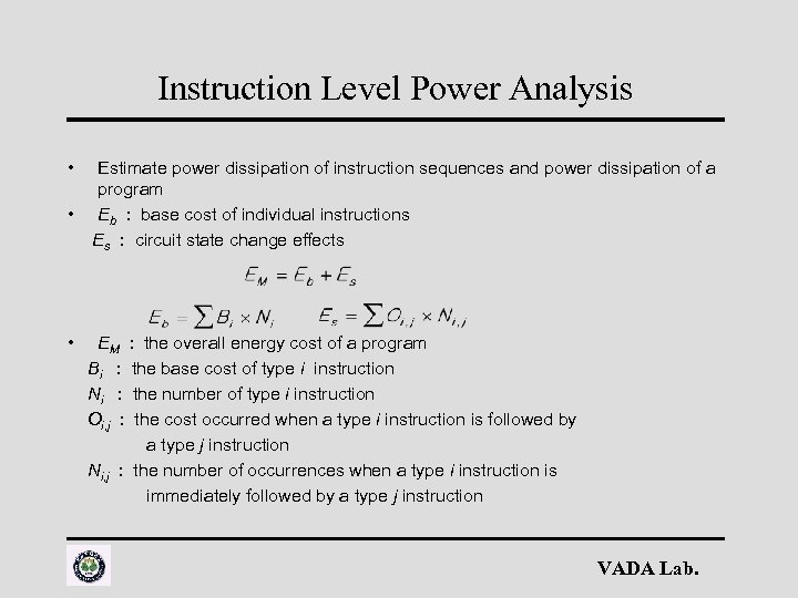 Instruction Level Power Analysis • • • Estimate power dissipation of instruction sequences and power dissipation of a program Eb : base cost of individual instructions Es : circuit state change effects EM : the overall energy cost of a program Bi : the base cost of type i instruction Ni : the number of type i instruction Oi, j : the cost occurred when a type i instruction is followed by a type j instruction Ni, j : the number of occurrences when a type i instruction is immediately followed by a type j instruction VADA Lab.
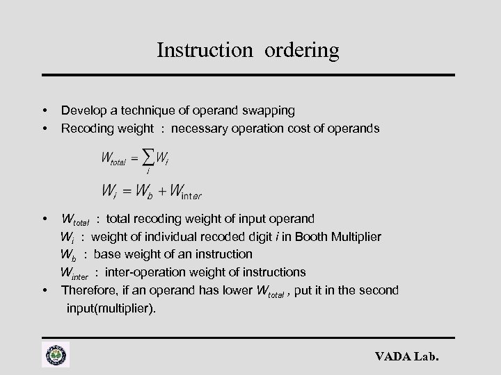 Instruction ordering • • Develop a technique of operand swapping Recoding weight : necessary operation cost of operands • Wtotal : total recoding weight of input operand Wi : weight of individual recoded digit i in Booth Multiplier Wb : base weight of an instruction Winter : inter-operation weight of instructions Therefore, if an operand has lower Wtotal , put it in the second input(multiplier). • VADA Lab.
 RESULT VADA Lab.
![Conclusion % of instances with circuit states effects 9. 0% reduction Power[p. J] 12. Conclusion % of instances with circuit states effects 9. 0% reduction Power[p. J] 12.](https://present5.com/presentation/9bfb1ca58853ea7141bd5ec1866f8ba3/image-126.jpg) Conclusion % of instances with circuit states effects 9. 0% reduction Power[p. J] 12. 0% reduction 4. 0% reduction bits VADA Lab.
Conclusion % of instances with circuit states effects 9. 0% reduction Power[p. J] 12. 0% reduction 4. 0% reduction bits VADA Lab.
 8. Layout Level Design Sung. Kyun. Kwan Univ. VADA Lab. 127
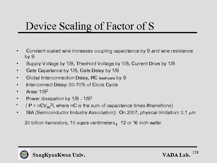 Device Scaling of Factor of S • • • Constant scaled wire increases coupling capacitance by S and wire resistance by S Supply Voltage by 1/S, Theshold Voltage by 1/S, Current Drive by 1/S Gate Capaitance by 1/S, Gate Delay by 1/S Global Interconnection Delay, RC load+para by S Interconnect Delay: 50 -70% of Clock Cycle Area: 1/S 2 Power dissipation by 1/S - 1/S 2 ( P = n. CVdd 2 f, where n. C is the sum of capacitance times #transitions) SIA (Semiconductor Industry Association): On 2007, physical limitation: 0. 1 m 20 billion transistors, 10 sqare centimeters Sung. Kyun. Kwan Univ. , 12 or 16 inch wafer VADA Lab. 128
 Delay Variations at Low-Voltage • At high supply voltage, the delay increases with temperature (mobility is decreasing with temperature) while at very low supply voltages the delay decreases with temperature (VT is decreasing with temperature). • At low supply voltages, the delay ratio between large and minimum transistor widths W increases in several factors. • Delay balancing of clock trees based on wire snaking in order to avoid clock-skew. In this case, at low supply voltages, slightly VT variations can significantly modify the delay balancing. Sung. Kyun. Kwan Univ. VADA Lab. 129
 Quarter Micron Challenge • • • • Computers/peripherals (SOC): 1996 ($50 Billion) 1999 ($70 Billion) Wiring dominates delay: wire R comparable to gate driver R; wire/wire coupling C > C to ground Push beyond 0. 07 micron Quest for area(past), speed-speed (now), power-power(future) Accelerated increases of clock frequencies Signal integrity-based tools Design styles (chip + packages) System-level design(system partitioning) Synthesis with multiple constraints (power, area, timing) Partitioning/MCM Increasing speed limits complicate clock and power distribution Design bounded by wires, via resistance, coupling Reverse scaling: adding area/spacing as needed: widening, thickening of wires, metal shielding & noise avoidance - adding metal Sung. Kyun. Kwan Univ. VADA Lab. 130
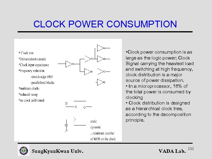 CLOCK POWER CONSUMPTION • Clock power consumption is as large as the logic power; Clock Signal carrying the heaviest load and switching at high frequency, clock distribution is a major source of power dissipation. • In a microprocessor, 18% of the total power is consumed by clocking • Clock distribution is designed as a hierarchical clock tree, according to the decomposition principle. Sung. Kyun. Kwan Univ. VADA Lab. 131
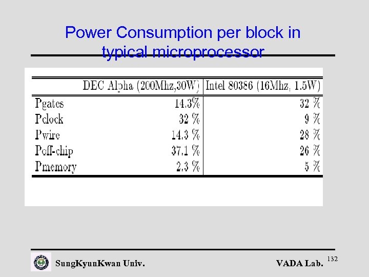 Power Consumption per block in typical microprocessor Sung. Kyun. Kwan Univ. VADA Lab. 132
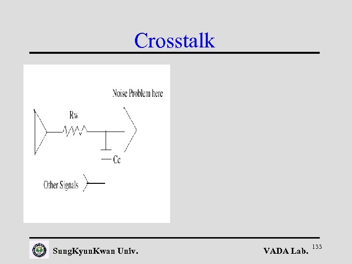 Crosstalk Sung. Kyun. Kwan Univ. VADA Lab. 133
 Solution for Clock Skew • • • Dynamic Effects on Skew Capacitance Coupling Supply Voltage Deviation (Clock driver and receiver voltage difference) Capacitance deviation by circuit operation Global and local temperature Layout Issues: clocks routed first Must aware of all sources of delay Increased spacing Wider wires Insert buffers Specialized clock need net matching Two approaches: Single Driver, Htree driver Sung. Kyun. Kwan Univ. • • Gated Clocks: The local clocks that are conditionally enabled so that the registers are only clocked during the write cycles. The clock is partitioned in different blocks and each block is clocked with its own clock. Gating the clocks to infrequently used blocks does not provide and acceptable level of power savings Divide the basic clock frequency to provide the lowest clock frequency needed to different parts of the circuit Clock Distribution: large clock buffer waste power. Use smaller clock buffers with a well-balanced clock tree. VADA Lab. 134
 Power. PC Clocking Scheme Sung. Kyun. Kwan Univ. VADA Lab. 135
 CLOCK DRIVERS IN THE DEC ALPHA 21164 Sung. Kyun. Kwan Univ. VADA Lab. 136
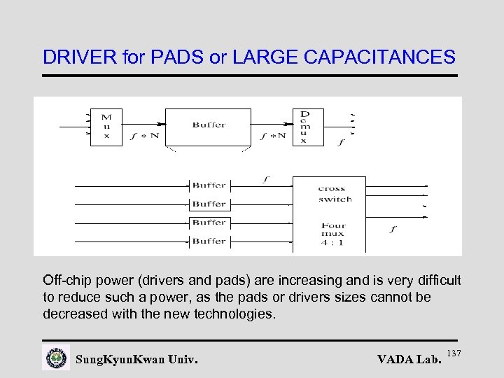 DRIVER for PADS or LARGE CAPACITANCES Off-chip power (drivers and pads) are increasing and is very difficult to reduce such a power, as the pads or drivers sizes cannot be decreased with the new technologies. Sung. Kyun. Kwan Univ. VADA Lab. 137
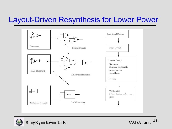 Layout-Driven Resynthesis for Lower Power Sung. Kyun. Kwan Univ. VADA Lab. 138
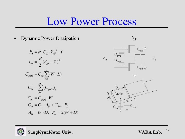 Low Power Process • Dynamic Power Dissipation Sung. Kyun. Kwan Univ. VADA Lab. 139
 Crosstalk • • • In deep-submicron layouts, some of the netlengths for connection between modules can be so long that they have a resistance which is comparable to the resistance of the driver. Each net in the mixed analog/digital circuits is identified depending upon its crosstalk sensitivity – 1. Noisy = high impedance signal that can disturb other signals, e. g. , clock signals. – 2. High-Sensitivity = high impedance analog nets; the most noise sensitive nets such as the input nets to operational amplifiers. – 3. Mid-Sensitivity = low/medium impedance analog nets. – 4. Low-Sensitivity = digital nets that directly affect the analog part in some cells such as control signals. – 5. Non-Sensitivity = The most noise insensitive nets such as pure digital nets, The crosstalk between two interconnection wires also depends on the frequencies (i. e. , signal activities) of the signals traveling on the wires. Recently, deep-submicron designs require crosstalk-free channel routing. 140 Sung. Kyun. Kwan Univ. VADA Lab.
 Power Measure in Layout • • • The average dynamic power consumed by a CMOS gate is given below, where C_l is the load capacity at the output of the node, V_dd is the supply voltage, T_cycle is the global clock period, N is the number of transitions of the gate output per clock cycle, C_g is the load capacity due to input capacitance of fanout gates, and C_w is the load capacity due to the interconnection tree formed between the driver and its fanout gates. Pav = (0. 5 Vdd 2) / (Tcycle Cl N) = (0. 5 Vdd 2) / (Tcycle (Cg + Cw )N) Logic synthesis for low power attempts to minimize SUMi Cgi Ni Physical design for low power tries to minimize SUMi Cwi Ni. Here Cwi consists of Cxi + Cs. I, where Cxi is the capacitance of net i due to its crosstalk, and Cs. I is the substrate capacitance of net i. For low power layout applications, power dissipation due to crosstalk is minimized by ensuring that wires carrying high activity signals are placed sufficiently far from the other wires. Similarly, power dissipation due to substrate capacitance is proportional to the wirelength and its signal activity. Sung. Kyun. Kwan Univ. VADA Lab. 141
 이중 전압을 이용한 저전력 레이아웃 설계 성균관대학교 전기전자컴퓨터공학부 김 진 혁, 이 준 성, 조 준 동 VADA Lab.
 목 • • • 차 연구목적 연구배경 Clustered Voltage Scaling 구조 Row by Row Power Supply 구조 Mix-And-Match Power Supply 구조 Level Converter 구조 Mix-And-Match Power Supply 설계흐름 실험결과 결론 VADA Lab.
 연 구 목 적 및 배경 • 조합회로의 전력 소모량을 줄이는 이중 전압 레이아웃 기법 제안 • 이중 전압 셀을 사용할 때, 한 cell row에 같은 전압의 cell이 배치되면 서 증가하는 wiring 과 track 의 수를 줄임 • 최소 트랜지스터 개수를 사용하는 Level Converter 회로의 구현 Sung. Kyun. Kwan Univ. • 디바이스의 성능을 유지하면서 이중 전압을 사용하는 Clustered Voltage Scaling [Usami, ’ 95]을 적 용 • 제안된 Mix-And-Match Power Supply 레이 아웃 구조는 기존의 Row by Row Power Supply [Usami, ’ 97] 레이 아웃 구조를 개선하여 전력과 면적을 줄임 VADA Lab. 144
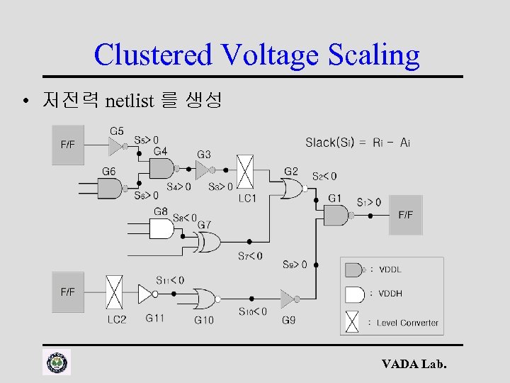 Clustered Voltage Scaling • 저전력 netlist 를 생성 VADA Lab.
 Row by Row Power Supply 구조 VADA Lab.
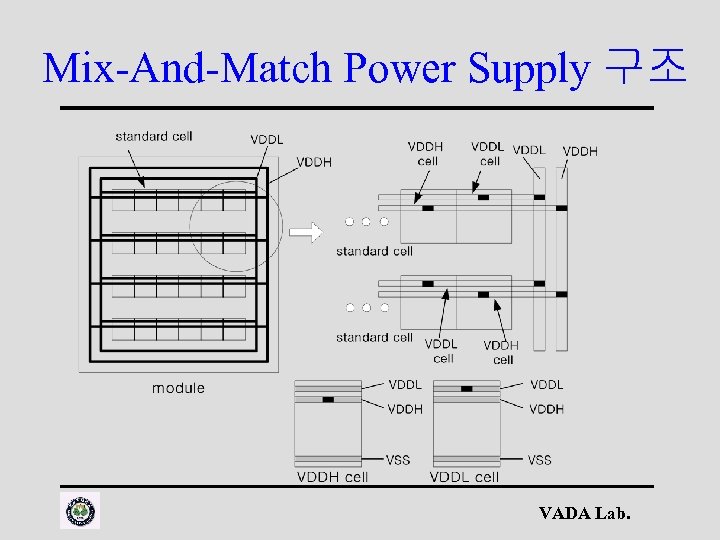 Mix-And-Match Power Supply 구조 VADA Lab.
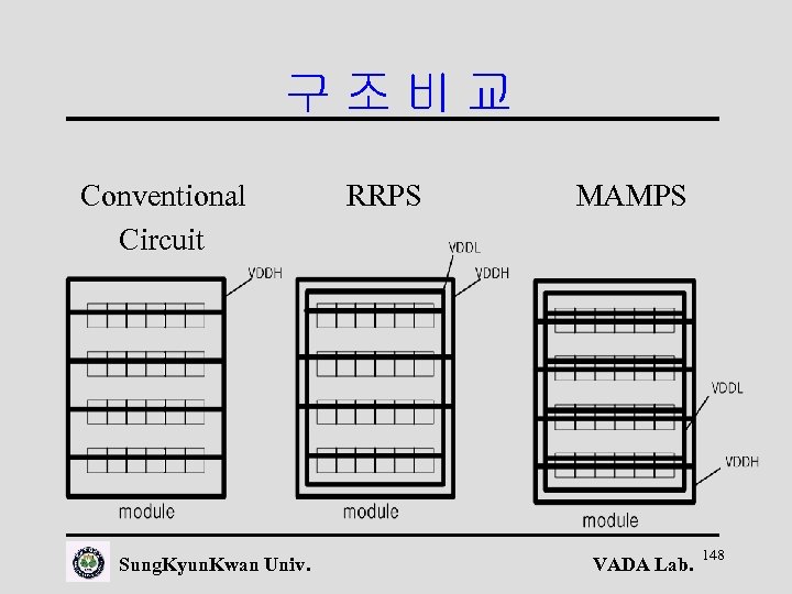 구조비교 Conventional Circuit Sung. Kyun. Kwan Univ. RRPS MAMPS VADA Lab. 148
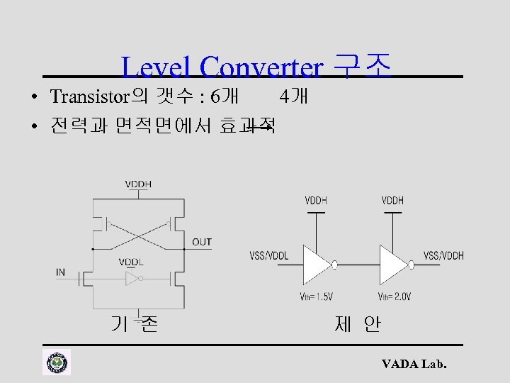 Level Converter 구조 • Transistor의 갯수 : 6개 4개 • 전력과 면적면에서 효과적 기 존 제 안 VADA Lab.
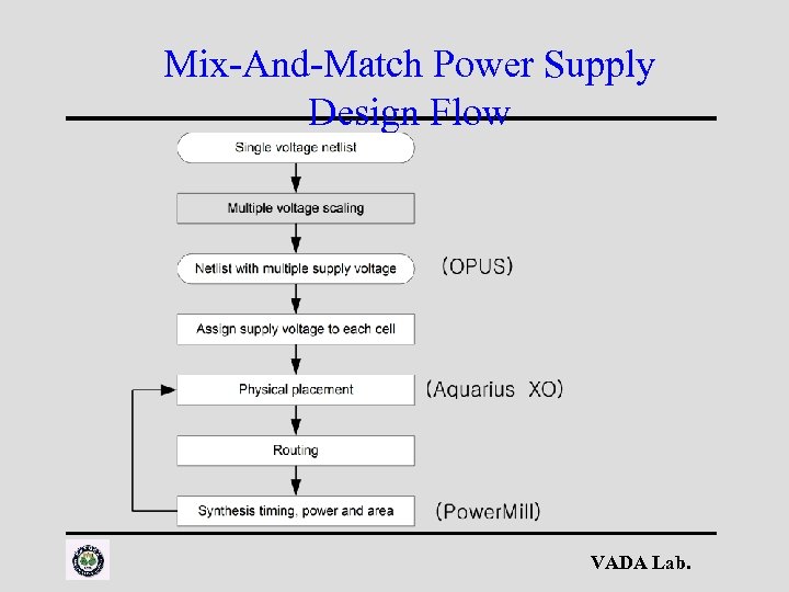 Mix-And-Match Power Supply Design Flow VADA Lab.
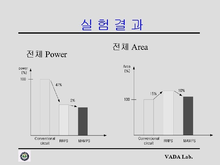 실험결과 전체 Power 전체 Area VADA Lab.
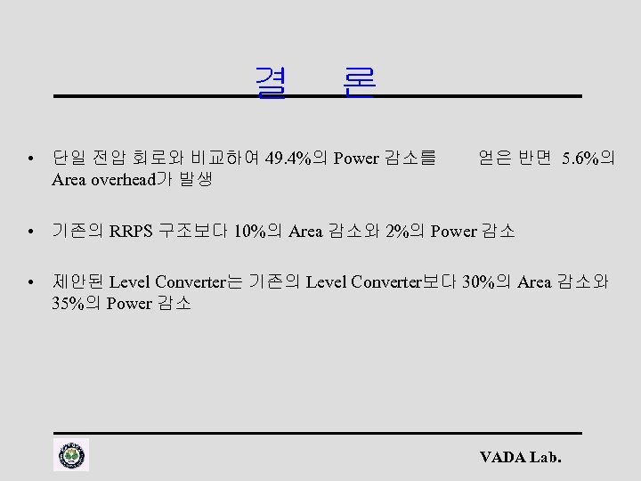 결 론 • 단일 전압 회로와 비교하여 49. 4%의 Power 감소를 Area overhead가 발생 얻은 반면 5. 6%의 • 기존의 RRPS 구조보다 10%의 Area 감소와 2%의 Power 감소 • 제안된 Level Converter는 기존의 Level Converter보다 30%의 Area 감소와 35%의 Power 감소 VADA Lab.
 9. CAD tools Sung. Kyun. Kwan Univ. VADA Lab. 153
 Low Power Design Tools • Transistor Level Tools (5 -10% of silicon) – SPICE, Power. Mill(Epic), ADM(Avanti/Anagram), Lsim Power Analyst(mentor) • Logic Level Tools (10 -15%) – Design Power and Power. Gate (Synopsys), Watt. Watcher/Gate (Sente), Power. Sim (System Sciences), POET (Viewlogic), and Quick. Power (Mentor) • Architectural (RTL) Level Tools (20 -25%) – Watt. Watcher/Architect (Sente): 20 -25% accuracy • Behavioral (spreadsheet) Level Tools (50 -100%) – Active area of academic research Sung. Kyun. Kwan Univ. VADA Lab. 154
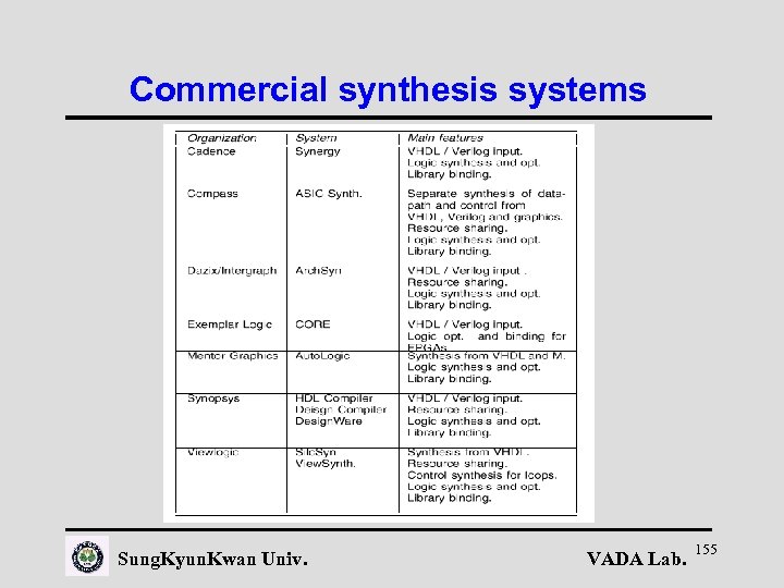 Commercial synthesis systems Sung. Kyun. Kwan Univ. VADA Lab. 155
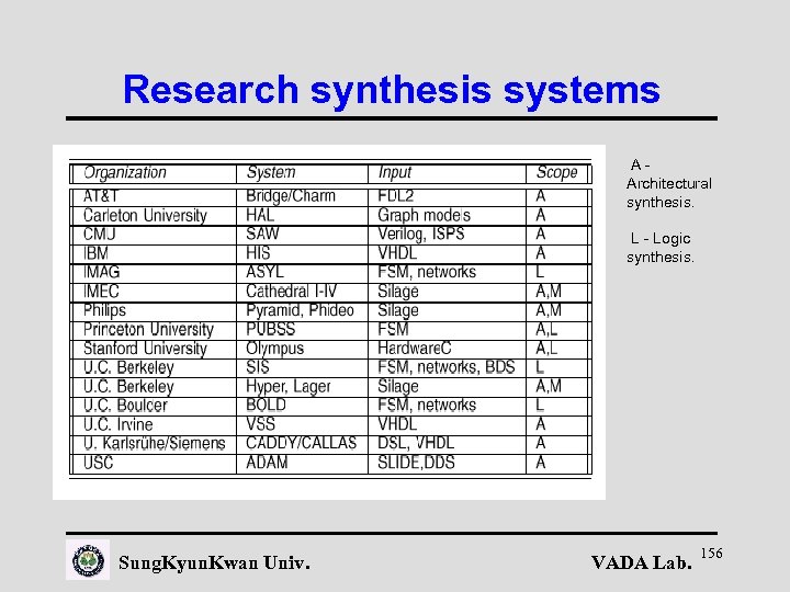 Research synthesis systems AArchitectural synthesis. L - Logic synthesis. Sung. Kyun. Kwan Univ. VADA Lab. 156
 Low-Power CAD sites • • • Alternative System Concepts, Inc, : 7 X power reduction throigh optimization, contact http: //www. ee. princeton. edu and Jake Karrfalt at jake@ascinc. com or (603) 437 -2234. Reduction of glitch and clock power; modeling and optimization of interconnect power; power optimization for data-dominated designs with limited control flow. Mentor Graphics Quick. Power: Hierarchical of determining overall benet of exchanging the blocks for lower powering down or disabling blocks when not in use by gated-clock choose candidates for power-down Calculate the effect of the power-down logic http: //www. mentorg. com Synopsys's Power Compiler http: //www. synopsys. com/products/power_ds Sente's Watt. Watcher/Architect (first commerical tool operating at the architecture level(20 -25 %accuracy). http: //www. powereda. com Behavioral Tool: Hyper-LP (Optimization), Explore (Estimation) by J. Rabaey Sung. Kyun. Kwan Univ. VADA Lab. 157
 Design Power(Synopsys) • • • Design. Power(TM) provides a single, integrated environment for power analysis in multiple phases of the design process: – Early, quick feedback at the HDL or gate level through probabilistic analysis. – Improved accuracy through simulation-based analysis for gate level and library exploration. Design. Power estimates switching, internal cell and leakage power. It accepts user-defined probabilities, simulation toggle data or a combination of both as input. Design. Power propagates switching information through sequential devices, including flip-flops and latches. It supports sequential, hierarchical, gated-clock, and multiple-clock designs. For simulation toggle data, it links directly to Verilog and VHDL simulators, including Synopsys' VSS. Sung. Kyun. Kwan Univ. VADA Lab. 158
 10. References Sung. Kyun. Kwan Univ. VADA Lab. 159
![References [1] Gary K. Yeap, References [1] Gary K. Yeap,](https://present5.com/presentation/9bfb1ca58853ea7141bd5ec1866f8ba3/image-160.jpg) References [1] Gary K. Yeap, "Practical Low Power Digital VLSI Design", Kluwer Academic Publishers. [2] Jan M. Rabaey, Massoud Pedram, "Low Power Design Methodologies", Kluwer Academic Publishers. [3] Abdellatif Bellaouar, Mohamed I. Elmasry, "Low-Power Digital VLSI Design Circuits And Systems", Kluwer Academic Publishers. [4] Anantha P. Chandrakasan, Robert W. Brodersen, "Low Power Digital CMOS Design", Kluwer Academic Publishers. [5] Dr. Ralph Cavin, Dr. Wentai Liu, "1996 Emerging Technologies : Designing Low Power Digital Systems" [6] Muhammad S. Elrabaa, Issam S. Abu-Khater, Mohamed I. Elmasry, "Advanced Low-Power Digital Circuit Techniques", Kluwer Academic Publishers. Sung. Kyun. Kwan Univ. VADA Lab. 160
References [1] Gary K. Yeap, "Practical Low Power Digital VLSI Design", Kluwer Academic Publishers. [2] Jan M. Rabaey, Massoud Pedram, "Low Power Design Methodologies", Kluwer Academic Publishers. [3] Abdellatif Bellaouar, Mohamed I. Elmasry, "Low-Power Digital VLSI Design Circuits And Systems", Kluwer Academic Publishers. [4] Anantha P. Chandrakasan, Robert W. Brodersen, "Low Power Digital CMOS Design", Kluwer Academic Publishers. [5] Dr. Ralph Cavin, Dr. Wentai Liu, "1996 Emerging Technologies : Designing Low Power Digital Systems" [6] Muhammad S. Elrabaa, Issam S. Abu-Khater, Mohamed I. Elmasry, "Advanced Low-Power Digital Circuit Techniques", Kluwer Academic Publishers. Sung. Kyun. Kwan Univ. VADA Lab. 160
![References • • • [BFKea 94] R. Bechade, R. Flaker, B. Kaumann, and et. References • • • [BFKea 94] R. Bechade, R. Flaker, B. Kaumann, and et.](https://present5.com/presentation/9bfb1ca58853ea7141bd5ec1866f8ba3/image-161.jpg) References • • • [BFKea 94] R. Bechade, R. Flaker, B. Kaumann, and et. al. A 32 b 66 mhz 1. 8 W Microprocessor". In IEEE Int. Solid-State Circuit Conference, pages 208 -209, 1994. [BM 95] Bohr and T. Mark. Interconnect Scaling - The real limiter to high performance ULSI". In proceedings of 1995 IEEE international electron devices meeting, pages 241 -242, 1995. [BSM 94] L. Benini, P. Siegel, and G. De Micheli. Saving Power by Synthesizing Gated Clocks for Sequential Circuits". IEEE Design and Test of Computers, 11(4): 32 -41, 1994. [GH 95] S. Ganguly and S. Hojat. Clock Distribution Design and Verification for Power. PC Microprocessor". In International Conference on Computer-Aided Design, page Issues in Clock Designs, 1995. [MGR 96] R. Mehra, L. M. Guerra, and J. Rabaey. Low Power Architecture Synthesis and the Impact of Exploiting Locality". In Journal of VLSI Signal Processing, , 1996. Sung. Kyun. Kwan Univ. VADA Lab. 161
References • • • [BFKea 94] R. Bechade, R. Flaker, B. Kaumann, and et. al. A 32 b 66 mhz 1. 8 W Microprocessor". In IEEE Int. Solid-State Circuit Conference, pages 208 -209, 1994. [BM 95] Bohr and T. Mark. Interconnect Scaling - The real limiter to high performance ULSI". In proceedings of 1995 IEEE international electron devices meeting, pages 241 -242, 1995. [BSM 94] L. Benini, P. Siegel, and G. De Micheli. Saving Power by Synthesizing Gated Clocks for Sequential Circuits". IEEE Design and Test of Computers, 11(4): 32 -41, 1994. [GH 95] S. Ganguly and S. Hojat. Clock Distribution Design and Verification for Power. PC Microprocessor". In International Conference on Computer-Aided Design, page Issues in Clock Designs, 1995. [MGR 96] R. Mehra, L. M. Guerra, and J. Rabaey. Low Power Architecture Synthesis and the Impact of Exploiting Locality". In Journal of VLSI Signal Processing, , 1996. Sung. Kyun. Kwan Univ. VADA Lab. 161


